ONE-CHIP VIDEO PROCESSOR
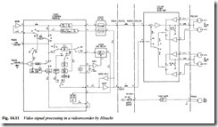
Later designs of VCR incorporate all the luminance and chrominance signal processing, for record and playback, in a single IC; a much simplified block diagram of a typical example for VHS is given in Fig. 14.11. It uses all the principles and many of the techniques described earlier in this chapter, and is teamed with a second IC which caters for video head amplification and equalisation, on both record and playback.
Entering at pin 7, the composite video signal for recording is split by chip-internal filters into its luminance and chrominance components. The Y signal leaves the chip on pin 46 for passage through Q208 stage, which contains an L/R/C shaping filter, then re-enters on pin 47, where it undergoes pre-emphasis and modulation onto the f.m. carrier. There are no preset controls involved at all
here, and the Y−f.m. signal passes out to the recording amplifier from pin 9 of IC203, an equaliser chip. Video E−E signals are looped through IC201 via a clamp, a buffer stage and IC pin 11. During replay the amplified off-tape signal enters the Y/chroma board at plug 231 pin 1, whence its luminance component is split off in a high-pass filter within IC203 for demodulation and de-emphasis within IC201: it enters on pin 43. Once more the baseband Y signal passes through filter/buffer stage Q208, now on its way to switch S8, set to PB position, and the dropout compensator, here represented by S7. Finally the luminance waveform is shaped, enhanced and sharpened before being added to the chrominance component and passed out of the IC via its pin 11. Thereafter it has on-screen characters added on its way to the AV-out sockets and r.f. modulator.
Tracing the record chrominance signal now, it is selected by chip- internal switch S5 and bandpass-filtered en route to the a.c.c. and frequency-conversion stages: it exits the chip via S6 and pin 38, pass- ing them into amplifier/response-shaping stage Q202. Within the video head-amplifier IC it is added to the Y−f.m. carrier which provides its ‘recording bias’, then the Y−C combination signal is writ- ten to tape. During replay the off-tape Y−f.m.+C signal coming from the video heads is initially buffered and filtered in the Q205/Q211 stages to derive a chroma signal at IC201 pin 38. A second filter within the chip produces ‘pure chroma’ on the colour-under carrier frequency of 627 kHz for a.c.c. regulation and up-conversion to 4.43 MHz. Now going via switch S5, the regenerated colour subcar- rier is ‘cleaned up’ – in the same filter as was used on record – on its way to S5, set to the lower position except in SECAM mode. The 2-line delay system, described before and used for chroma crosstalk cancellation, is here embodied in the electronic (bucket-brigade) CCD device IC202 between pins 17 and 21 of the main chip; the charges are stepped through it by a subcarrier-based clock pulse entering on its pin 12. A colour-killer stage and final filtering sees the chroma signal ready for addition to the Y/luminance component of the composite signal which passes out of the chip on pin 11.
In this necessarily abridged description and grossly simplified diagram, many of the processes which go on inside the chip (and are therefore not accessible anyway!) are not shown. Thus the crystal oscillator at IC pins 27/28 drives and times many functions within the chip, including the four-phase manipulation section which formed such important parts of Figs 14.6 and 14.8, but does not appear in this diagram – it is there, together with the other devices and artifices described earlier in this chapter.
