THE PAL VARIANT
The process so far described is a greatly simplified version of the first colour encoding system to be used, type NTSC. It works well, but has the drawback that if any level-dependent delay is present in the transmission chain – including any video tape machine used for ‘storage’ – the burst and signal-chroma components of the CVBS signal will, because they pass at different levels through the system, be treated differently. Since the correct reproduction of colour hue depends entirely on the maintenance of correct phase between these two, pictures transmitted over difficult paths by the NTSC process can suffer hue errors, necessitating a subcarrier phasing control (hue adjustment) at the receiver. To overcome this problem a modification of the basic NTSC system (PAL, Phase Alternation Line) was introduced in many countries.
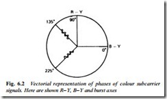
In the PAL system the phase of the subcarrier conveying the R−Y signal is reversed on a line-by-line basis. This can be achieved by inverting either the subcarrier signal or the R−Y signal itself before entry to the suppressed carrier modulator. It offers the opportunity to cancel out hue errors due to differential phase distortion in the transmission path by means of a delay-line circuit in the receiver’s decoder; more details will be given in the next chapter. To signal to the receiver’s decoder which line carries the ‘inverted’ R−Y waveform an identification (ident) signal must now be added to the chroma signal for transmission. It is done by advancing the phase of the colour-burst cycles by 45° on ‘PAL’ (inverted R−Y) lines, and retard- ing their phase by 45° on the other (‘normal’) lines. The mean phase of the burst signal remains at 180°, corresponding to −(B−Y), but advances to 225° and retreats to 135° (see Fig. 6.2) on alternate lines – hence the expression ‘swinging burst’.
CAMERA BASICS
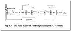
A block diagram of the luminance chain of a simple colour TV camera is given in Fig. 6.3. From the image-sensor or -source, whatever form it may take, three separate primary-colour video signals are produced. They are amplified in low-noise FET preamplifiers and passed to attenuators as previously described for derivation of the correct proportions of Y signal. An adder combines these into a Y signal for application to the video amplifier.
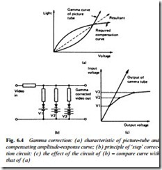
To prevent drift of the Y signal’s black level with picture content, time, and temperature, a clamp is next encountered, in which the d.c. level of the waveform is returned to a fixed voltage during line and field blanking intervals. Spurious signals during the blanking intervals are suppressed by the blanking system at this point. Following further amplification the Y signal undergoes a gamma correction process. Whereas the most commonly used image pick-up sensors render a voltage output proportional to light input (gamma value 1) the
picture-tube which will be used to reproduce the picture has a non- linear voltage input/light output curve (gamma value about 2.2, see Fig. 6.4(a)) which, if no compensating steps were taken, would result in a compression of contrast steps in the dark regions of the picture, and a ‘stretching’ of them in the lighter areas. Correct reproduction in monochrome and in colour requires the use in the camera of a non-linear amplifier called a gamma corrector, in which an equal- and-opposite input/gain characteristics (1/2.2) is introduced. The required curve (Fig. 6.4(a)) can be achieved with a ladder-network of diodes, resistors and reference voltages as in Fig. 6.4(b)). As new reference voltages V1, V2, V3 are attained by the video signal, progressively more diodes come into circuit to shunt away the signal and reduce its level – Fig. 6.4(c)).
Next in the luminance circuit comes a contour enhancer or aperture corrector. Because the image sensor has a finite pixel size its scan across a sharp black/white transition in the picture gives rise to a sloping edge in the video waveform rather than a ‘square’ signal transition. To subjectively compensate for the ‘softening’ of the picture thus introduced, the start and finish points of each picture feature are emphasised by the addition to the video waveform of suit- ably polarised spikes to give both pre-shoot and overshoot. This is achieved by means of a short delay line, differentiators, inverters and adders. These ‘crispening’ circuits – contour enhancers – can also be made, in conjunction with a one-line/64 μs delay, to sharpen horizontal edges of picture features.
The function of the next block in Fig. 6.3 is to delay the entire luminance signal by about 0.5 μs. As we shall shortly see, the bandwidth of the chrominance signal channel in the camera is restricted to about 500 kHz, which has the effect of delaying the chroma signals. To ensure that the edge-lines of both luma and chroma picture components coincide in the CVBS waveform and on the viewing screen this short delay is introduced in the Y signal path. In the following blocks are added the composite sync pulses and
the chroma component, which already incorporates the swinging burst signal. The CVBS signal is now complete and passes to an emitter-follower buffer stage with an output impedance of 75 Ω for passage out of the camera section to a videorecorder, monitor or r.f. modulator.


