Driving the panel
The process of driving a plasma panel follows the sequence of ADS described above. First, the set voltage is applied simultaneously to all the pixels and their individual cells. Next, the pixels are addressed one line at a time. Each line is selected in turn and the pixel cells along that line are addressed individually by the digitised video data fed down the address electrode bus. If a particular cell in that line is to be selected for discharge, then the dielectric in that cell is charged and a wall charge is formed. Once the pixel cells have been addressed and the appropriate cells primed by a wall charge, the next line is selected and the cells in that line are addressed and primed as dictated by the next set of video data clocked down the address columns and so on.
When all the lines have been scanned and all the pixel cells addressed and primed as necessary, the sustain phase is then executed by applying a series of sustain pulses to all S electrodes and a similar but anti-phase
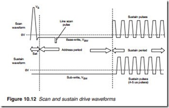
sustain pulses to the common C electrodes. The scan and sustain wave- forms will thus have the distinctive shapes shown in Figure 10.12. A set voltage pulse VS is applied to all scan electrodes simultaneously to clear and set all pixel cells. This is then followed by the address or write period in which, each line or row of pixels is selected in turn by a negative going select pulse. The cells along the selected line are then addressed and primed by one-bit video data fed down the address bus, hence the name one-bit plane technique. A video data bit of 1 will select the cell for emission and a wall charge will be formed. A data bit of 0 will not select the cell and wall charge will not be formed. After the line has been addressed, its scan voltage is kept at a negative voltage known as base-write voltage VBW for the remaining duration of the address period. This is necessary in order to avoid pre-mature discharge of the cells, known as self-erasing discharge which will remove the wall charge. As for the sustain electrode, it is kept at a small negative voltage known as sub-write voltage VSW during the address period. At the end of the address period, out-of-phases 4–5 Jls pulses are fed into the sustain and scan electrodes for the simultaneous discharge and display of all selected pixel cells.
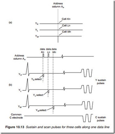
Figure 10.13b shows the waveforms associated with addressing three pixel cells, KN, LN and MN on three consecutive lines, YK, YL and YM respec- tively. All three cells fall along the same address line An (Figure 10.13a). At the set phase, a set pulse is fed to all scan lines. The address phase involves selecting each line separately by a negative going pulse. Pixel line YK is selected by YK select pulse and at the same time, data for pixel cell Kn appears on address line An to prime the cell for discharge during the sus- tain phase. Pixel line YL is then selected by YL select and simultaneously data Ln appears on address bus An to prime the cell. Similarly for pixel line YM except that in this case the data for cell Mn is zero and the cell is not
Plasma panels primed for discharge. When the scan phase is completed, anti-phase sustain pulses are applied to the Y and C electrodes.

