Address display separated
Driving a pixel cell involves three phases (Figure 10.7):
● set or initialise (also known as erase),
● address or write,
● sustain or discharge (also known as display).
The set phase
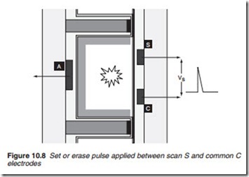
The cell is set by removing any residual charge that may remain from a previous drive cycle. This is accomplished by applying a step pulse in the region of 300–400 V, between the scan (S) and common sustain (C) electrodes
(Figure 10.8). The step voltage causes a small start discharge to take place and the gas in the cell becomes ionised. This start discharge is not a fully fledged discharge and very low light emission occurs.
The address phase
Once the cell has been cleared and set, the next stage is to determine if the cell is required to be ‘turned ON’, i.e. required to produce light emission. This depends on the picture content represented by the video information fed into the address (A) electrode. At this stage, the scan (S) electrode is taken to a negative potential by a scan pulse. If the data electrode is at logic 1, then the cell is selected for emission. The potential between the data and scan electrode causes a small discharge to take place in the cell. The dis- charge is quickly quenched as the dielectric surrounding the electrodes charges up. This charge is known as the ‘wall charge’ which primes the cell for a fully fledged plasma discharge at the next phase (Figure 10.9). The pixel cell that does not have a wall charge will not produce light at the next phase. This technique in which the active cells are selected by forming a wall charge at the address stage is known as ‘selective write’ addressing.
The sustain phase
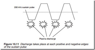
The final stage is to discharge the cell and produce light emission. This is accomplished by applying a high frequency pulse (in the region of 200 kHz) known as the sustain pulse between the scan S and the common sustain
C electrodes. The amplitude of the sustain pulse is smaller than the break- down voltage of the plasma. However, its polarity is such as to add to the existing wall charge causing plasma discharge to take place and with it the emission of UV which upon bombarding the phosphor coating release the appropriate colour glow (Figure 10.10). This discharge will also be quenched by the dielectric creating a new wall charge. This time, however, the wall charge is in the reverse polarity to the previous one. If now a sustain pulse with an opposite polarity is applied to the scan-sustain electrodes,
it will add to the newly created wall charge to produce another full dis- charge which in turn reverses the wall charge and so on. Discharge will thus occur at each positive and negative halves of the sustain pulse as illustrated in Figure 10.11. The brightness of the pixel cell is determined by the number of sustain pulses applied to the electrodes. If the cell was not selected for emission during the address phase, there would not be a wall charge and a pixel cell discharge will not occur even when a sustain pulse is applied.
From the above, it can be seen that the set–address–discharge process have three distinct and separate phases. This technique is known as address display separated (ADS) in which pixel cells are ‘addressed’ individually and then in a ‘separate’ phase the pixels are ‘displayed’ by a simultaneous discharge.


