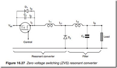
Zero voltage switching
A resonant converter which uses ZVS is illustrated in Figure 16.27 with L2/C2 forming a low-pass filter. In the steady-state condition, load current I0 is equal to the current through L2. Starting with the MOSFET on, its cur- rent IT and IL1 are equal to IL2 and Diode D2 is reverse biased. The voltage across the MOSFET is zero. When the transistor is turned off by a control pulse to its gate, current is diverted into C1. Capacitor C1 charges up until, when fully charged, diode D2 becomes forward biased and conducts and C1 and L1 begin to oscillate going up to a peak after which, the voltage
across C1 attempts to reverse and diode D1 starts conducting. During this time, the MOSFET is triggered to conduct, but remains off while D1 is on. As soon as D1 turns off when IL1 drops to zero and begins to reverse, the transistor turns on (ZVS) and remains on until it is turned off by a pulse and so on. The MOSFET turns off naturally and is turned on by a pulse,
i.e. ‘fixed off-time, varied on-time’.
A circuit diagram for a resonant converter used to supply the sustain voltage for a 42 in. plasma panel is shown in Figure 16.28. Two pairs of back-to-back Power MOSFETs Q12/Q15 and Q13/Q14 are used as the switching transistors driven by Q10 and Q11. They are fed with 400 V d.c.
from a flyback converter. Two anti-phase PMW control pulses arrive from the control panel to Q2 and Q3 to control the switching of each pair. The output for the sustain and the scan electrodes of the plasma panel are provided full-wave rectifiers connected to the secondary of the output trans former. Feedback to the control panel is obtained via Q6 and Q7. Although power MOSFET have been used almost universally, current-driven insulated gate bipolar transistors (IGBT) (Figure 16.29) may also be used.
