Linear regulators
A simple linear series regulated power supply is shown in Figure 15.2, in which TR1 is the regulator. Load regulation is obtained by zener diode Z1, which provides the reference voltage for the base of common-emitter
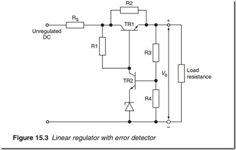
transistor TR1. Z1 maintains the base of TR1 at a constant potential established by its breakdown voltage. The d.c. output taken at the emitter is thus maintained at 0.6 V below the zener voltage. Changes in the output level produce changes in the b–e bias of the transistor in such a way as to keep the output constant. For higher load currents, a Darlington pair may be used, normally as an IC package. Sensitivity and response may be improved by using an error detector as shown in Figure 15.3. TR1 is the normal series regulator. TR2 compares a portion of the output voltage with the reference voltage of e zener. Changes in the output level are
amplified and fed into the base of TR1, which maintains the output con- stant. A shunt bypass also known as ‘bleeding’ resistor, R2, is sometimes connected across the c–e junction of TR1 to reduce the power dissipation of the series regulator by diverting a portion of the load current away from the transistor. It also provides the initial start-up voltage for the regulator by ‘bleeding’ the current across TR1 to the output; this provides the necessary potential for TR2 and the zener to begin to conduct and start the regulator functioning.

