6.1 THE Z80 PROGRAMMING MODEL

6.1 THE Z80 PROGRAMMING MODEL

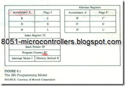
In Chapter 2, we developed a model to represent the internal structure of the MPU shown in Figure 2.3. We will now describe a similar model of the Z80 micropro­cessor; however, we will include only those components necessary for the pro­grammer. Figure 6.1 shows such a model, which includes an accumulator and a flag register, general-purpose register arrays, registers used as memory pointers,

z80 Interfacing and programming-34_03

z80 Interfacing and programming-35_03

and special-purpose registers. These registers and their functions were described briefly in Chapter 3 in the context of the Z80 architecture; now, they are described in detail in the following sections.

6.1.1 Accumulator

The accumulator is an 8-bit register that is part of the Arithmetic/Logic unit (ALU) and is also identified as register A. This register is used to store 8-bit data and to perform arithmetic and logic operations. The result of an operation performed in the ALU is also stored in the accumulator. For example, in an 8-bit addition, the instruction ADD always assumes that one of the numbers is the byte in the accumulator. and the result of the addition is stored in the accumulator by replacing the previous byte.

Figure 6.1 shows an additional accumulator called A’ in the alternate register set. A’ is not directly accessible to store a byte or perform an ALU operation, but the contents of A’ are accessible by using the exchange instruction EX AF,AF’.

6.1.2 Flag Register

The ALU includes, six flip-flops that are set or reset according to data conditions after an ALU operation, and the status of each flip-flop, also known as flags, is shown in the flag register F. The status of each of the six flags is stored in the 8­bit flag register so that they can be examined if necessary. The bit position of each flag is shown in Figure 6.2; bits D5 and D3 are unused.

Among the six flags, the H (Half-Carry) and N (Add/Subtract) flags are used .internally by the microprocessor for BCD (Binary Coded Decimal) operations.

These two flags cannot be tested by any instruction and are not available to the programmer for decision making. The remaining four flags-S (Sign), Z (Zero), P/V (Parity/Overflow), and C (Carry)* -can be tested in conjunction with Con­ditional Jump or .Call instructions. Each of these four flags has two Jumps or Call instructions associated with it: one when the flag is set and the other when the flag is reset. These flags have critical importance in the decision-making process;

all decisions are based on the status of these flags. For example, the instruction JP C, 2050H (Jump on Carry to memory location 2050H) is implemented to change the sequence of a program when the Carry flag is set.

The details of these flags are described below in the order of frequency of use. They will be discussed again in the context of illustrative programs. At the outset. The descriptions of these flags may appear quite complex. However, when we begin to write programs, we will see that, in general, most flags are ignored except one or two depending upon the operations being performed. For the time being, to understand their function, you should focus on three flags: C (Carry), Z (Zero). and S (Sign).

Ø C-Carry flag: If an arithmetic operation generates a carry (in addition) or a borrow (in subtraction), the Carry flag is set; otherwise it is reset.

It is important to remember that when an arithmetic operation does not gener­ate a carry (or borrow), the flag is reset.

The flag is also affected by such other ; instructions as logic and shift instruc­tions. The details will be discussed when specific instructions are explained. The Z80 includes instructions SCF-Set Carry Fla8-and CCF- Complement Carry Flag-that can set or complement this flag independent of the previous ALU operation.

Ø Z-Zero flag: If an 8-bit operation results in zero, the Z flag is set; otherwise it is reset.

In a bit testing operation, if the bit is zero, this flag is set; otherwise it is reset. In comparing two numbers, the Z flag is set when they are equal; otherwise it is reset.

The Z flag is also affected by special input instructions, block I/O instructions, and counting instructions.

Ø S-Sign flag: After an ALU operation, if the most significant bit D7 is 1, the sign flag is set; otherwise it is reset. When the flag is set, you do not necessarily have a negative result. The interpretation of the Sign flag depends upon the number system (unsigned number, signed magnitude, or 2’s complement) being used by the programmer. This flag can, of course, be used to indicate negative numbers, but its usage can be confusing. Therefore, it is discussed in detail in the context of the appropriate instructions. This flag is also affected by special input instructions in the Z80 set.

Ø P/V-Parity/Overflow flag: This flag is used for two purposes: to check the parity (the number of Is in a byte) and to check an overflow in dealing with signed numbers.

In the case of a parity check after an operation, if the number of ls in the result is even (even parity), this flag is set, and if the number of ls is odd (odd parity), the flag is reset. For example, if the result of ANDing two bytes is 0 0 0 0 0 0 11, the parity flag is set to indicate even parity (two ls). In this example, the magnitude base-ten (310) is odd; however, the odd or even number has no relationship with the odd or the even parity.

In arithmetic operations of signed numbers where bit D7 is used to indicate sign, this flag is set to indicate an overflow condition. For example, when bit D7 is reserved for a sign, the magnitude of a number is represented by the remaining seven bits, the maximum being 01 1 1 1 1 1 1 (+ 12710), After an addition, if the sum goes beyond + 127,bit D7 changes to l, a change that would indicate a negative result. In fact, this is an overflow condition and it is indicated by the overflow (V) flag,

This flag is also used for other functions such as block transfer, search, and interrupt.

Ø H-Half-Carry flag: In an arithmetic operation, this flag is affected by the carry or borrow between bits D3 and D4.In addition, when there is a carry from bit D3 to D4,the Half-Carry flag (H) is set; otherwise, it is reset. In a subtraction, when there is a borrow from bit D4 to D3, this flag is set; otherwise, it is reset. The flag is used internally for BCD (Binary Coded Decimal) operations, and there are no Jump or Call instructions associated with this flag.

Ø N-Add/Subtract flag: This flag is also used internally for BCD operations to distinguish between addition and subtraction. For BCD addition, this flag is 0 and for subtraction it is set to l ,

The alternate flag register F’ is associated with the alternate accumulator A’ as shown in Figure 6.1. The contents of this register can be accessed by using the exchange instruction.

6.1.3 General- Purpose and Alternate Registers

The Z80 microprocessor has six programmable general-purpose registers named B, C, D, E, H, and L, as shown in Figure 6. I. These are 8-bit registers used for storing data during the program execution. They can be combined as register pairs-BC, DE, HL- to perform 16-bit operations or to hold memory addresses.

The programmer can use these registers to load or copy data. For example, the instruction LD B, C copies the data from register C into register B, Concep­tually, these registers can be viewed as memory locations, except that they are built inside the microprocessor and identified by specific names. Some micropro­cessors do not have this type of register; instead, they use memory as their registers.

In addition to the general-purpose registers, the Z80 includes a similar set of six alternate registers designated as B’, C’, D’, E’, H’, and L’. They are not di­rectly available to the programmer, except through the exchange instructions; The contents of general-purpose register pairs can be exchanged with the alternate register pairs.

6.1.4 16-Bit Registers as Memory Pointers

The Z80 microprocessor includes four 16-bit registers used to hold memory ad­dresses; they are classified here as memory pointers. The primary function of memory is to store instructions and data, and the microprocessor needs to access Memory registers to read these instructions and data. To access a memory regis­ter, the microprocessor identifies the register by using the addresses in these memory pointers.

INDEX REGISTERS (IX AND IY)

The Z80 has two 16-bit index registers called IX and IY. Each register is used to specify a memory address by the 16-bit address it holds and a displacement count. For example, if the IX register holds 2050H; a higher memory address such as 2060H can be specified by adding the displacement count of 10H. Similarly, a lower memory address such as 2040H can be specified by adding the negative of 10H in 2’s complement.

In addition to the index registers, the HL Pair is frequently used as a memory pointer. Similarly, the BC and DE pairs can used also memory pointers in a limited way. However, no displacement byte can be added to the contents of these pairs.

STACK POINTER (SP)

The stack pointer is also a 16-bit register used to point to the memory location called the stack. The stack is a defined area of memory locations in R/W memory, and the beginning of the stack is defined by loading a 16-bit address into the stack

pointer.

We will discuss the concept of the stack memory in detail when we introduce the topic of subroutines.

PROGRAM COUNTER (PC)

This register functions as a 16-bit counter. The microprocessor uses this register to sequence the execution of instructions. The program counter points to the memory address from which the next byte is to be fetched, and when the micro­processor places an address on the address bus to fetch the byte from memory, it then increments the program counter by one to point to the next memory location.

6.1.5 Special-Purpose Registers

The Z80 microprocessor includes two special-purpose registers, generally absent in other 8-bit microprocessors. These registers are shown in Figure 6.1 as interrupt vector register (I)and the memory refresh register (R).

INTERRUPT VECTOR REGISTER (I)

This is an 8-bit register used in the interrupt process. When an external device interrupts the microprocessor with a request to do something else, the micropro­cessor should be directed to a 16-bit address in memory where it can find what to do next. The I register is used to store the high-order eight bits of the 16-bit address; the low-order eight bits must be supplied by the interrupting device . We will discuss the details and applications of this register in chapter 12.

MEMORY REFRESH REGISTER (R)

The memory refresh register (R) is also an 8-bit register that is used as a 7-bit counter to provide an address of memory cells to be refreshed in dynamic mem­ory. "As mentioned in Chapter 2, information stored as a capacitive charge in dy­namic memory leaks; therefore, bit information should be refreshed, meaning it should be read and stored again every few milliseconds. Applications of the mem­ory refresh register (R) will be discussed in detail with the topic of Interfacing Dynamic Memory. ‘
 

Introduction to Z80 Assembly Language Programming

Introduction to Z80 Assembly Language Programming

An assembly language program is a set of in­structions, written in the mnemonics of a given microprocessor, and in a sequence appropriate to a specified task. To write such programs, we should be familiar with the programming model (internal registers) of the microprocessor and its instruction set. This chapter introduces the Z80 programming model and provides such an over­view of the Z80 instruction set.

The Z80 instruction set is classified into six categories, and each category is explained with examples. The chapter also discusses the instruction format and various addressing modes, Writing, assembling, and executing a program are illustrated by a simple problem of adding two Hex numbers. The flowcharting technique and symbols are discussed in the context of the illustrative program. The chap­ter concludes with a list of selected Z80 instructions:

OBJECTIVES

· Draw the Z80 programming model and iden­tify the registers.

· Explain the functions of the accumulator, general-purpose registers, and alternate reg­isters.

· Explain the functions of 16-bit registers and special-purpose registers.

· List the flags and explain the data conditions under which they are set or reset.

· Explain the terms operation code (opcode) and operand, and illustrate these terms by writing instructions.

· Classify the instructions in terms of their word size and specify the number of memory registers required to store the instructions in memory.

· List the six categories of the Z80 instruction set.

· Define and explain the term addressing mode.

· Write logical steps needed to solve a simple programming problem.

· Draw a flowchart from the logical steps of a given programming problem.

· Write mnemonics from the flowchart and convert the mnemonics into Hex code for a given programming problem.


introduction to assembly language programming of z80

is an introduction to Z80 assembly language programming. It explains commonly used instructions, elementary pro­gramming techniques and their applications, and the modular approach to software design.

The content is presented in a format sim­ilar to one for learning a foreign language. One approach to learning a foreign language is to be­gin with a few words that can form simple, meaningful, and interactive sentences. After learning a few sentences, one begins writing paragraphs that can convey ideas in a coherent fashion; then, by sequencing a few paragraphs, one can compose a letter. Chapters 6 to 11 are arranged in similar fashion-from simple in­structions to applications.

. Chapter 6 presents the Z80 programming model and provides an overview of the Z80 in­struction set and its capability. Chapter 7 deals with software development systems and Z80 as­semblers. Chapters 8 and 9 are concerned primarily with the Z80 instructions that occur most frequently. The instructions are not intro­duced according to the six groups as classified in Chapter 6; instead, a few instructions that can perform simple tasks are selected from each group. Chapter 8 includes the discussion of instructions from three groups–data copy. Arithmetic, and branch-and their various ap­plications. Chapter 9 introduces logic and bit manipulation instructions and their applica­tions. Chapter 10 introduces the concepts of subroutine and stack, which provide flexibility and variety for program design. Chapter 11 syn­thesizes the programming concepts presented in earlier chapters by illustrating application programs and demonstrates the modular ap­proach to software design.

PREREQUISITES

The reader is expected to know the following topics (refer to Chapters 1 and 2):

· Concepts in microprocessor architecture.

· Concepts related to memory and I/Os.

· Logic operations and binary and hexadeci­mal arithmetic.


ASSIGNMENTS ON INTERFACING I/O DEVICES

ASSIGNMENTS

1. Explain why the number of output ports in peripheral-mapped I/O is re­stricted to 256 ports.

2. In peripheral-mapped I/O, can an input port and an output port have the same port address?

3. If an output and input port can have the same 8-bit address, how does the Z80 differentiate between the ports?

4. Specify the two control signals required to latch data in an output port.

5. Specify the type of pulse required to latch data in the 7475.

6. Are data latched in the 7475 at the leading edge, during the level, or at the trailing edge of the enable (E) signal?

7. If the control signals W̅R̅ and I̅O̅R̅Q̅ are asserted at the same time, can data be latched using only the control signal W̅R̅?

8. If the answer to the previous question is yes, what are potential problems with the interfacing circuit?

9. In Figure 5.4, explain why the LED cathodes rather than anodes are con­nected to the latch.

10. Specify the control signals required to enable an input port.

11. Explain why a latch is used for an output port, but a tri-state buffer can be used for an input port.

12. What are the control signals necessary in memory-mapped I/O?

13. Can the microprocessor differentiate whether it is reading from a memory ­mapped input port or from memory?

14. In Figure 5.11, connect the output of the comparator to data line D7 and also drive the transistor with bit D7 • Make the necessary changes in the instructions.

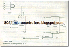
15. Identify the port address in Figure 5.13.

16. In Figure 5.13, if O̅E̅ is connected directly to the W̅R̅ signal and the output of the decoder is connected to the latch enable (through an inverter), can you display a byte at the output port? Explain your answer.

z80 Interfacing and programming-27_03


z80 Interfacing and programming-28_03

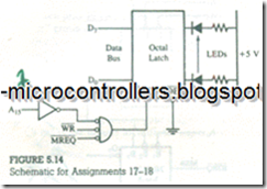
17. In Figure 5.14, determine whether it is the memory-mapped or the peripheral-mapped I/O.

18. In Figure 5.14, what is the port address if all the "don’t care" address lines are assumed to be at logic 0?

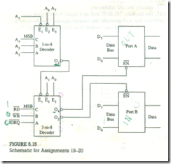
19. In Figure 5.15, are ports A and B input or output ports?

20. In Figure 5.15, what are the addresses of ports A and B?

Untitled-28_03


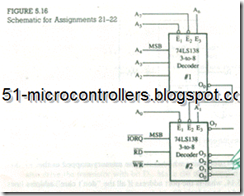
21. In Figure 5.16, identify two output lines of decoder #2 that can be used as control signals and explain their functions. Explain why other output lines cannot be used as control signals.

22. In Figure 5.16, specify the I/O addresses.

23. In Figure 5.17, the decoder 74LS155 and an 8-input NAND gate are used to decode the address bus and generate the control signals. The decoder has two input lines (A1 and A0) and four enable lines (pins 1,2,14, and 15).

z80 Interfacing and programming-29_03

When pins 14 and 15 (active low) are enabled, the four output lines of the "b" group decode the input signal, and when pins 1 (active high) and2 (ac­tive low) are enabled, the four output lines of the "a" group decode the in­put signals. Identify the addresses that can assert the output lines of the de­coder and specify their I/O functions.

24. Sketch the waveforms of the M1 cycles in the diagnostic routine (section 5.8).

25. Write a similar diagnostic routine to test the circuit in Figure 5.8

26. Is there a W̅R̅ pulse in your diagnostic routine of 25? If the answer is no, what is the unique identifiable signal that can be used to sync the scope?


SUMMARY OF INTERFACING I/O DEVICES

SUMMARY

in this chapter, we have examined the machine cycles of the OUT and IN in­structions and derived the basic concepts for interfacing peripheral-mapped I/Os. Similarly, we examined the machine cycles of memory-related data trans­fer instructions and derived the basic concepts for interfacing memory-mapped I/Os. These concepts were illustrated with three examples of interfacing I/O de­vices and one example of interfacing an analog signal. The interfacing concepts can be summarized as follows.

Peripheral-Mapped I/O

· The OUT is a 2-byte instruction and copies (transfers or sends) data from the accumulator to the addressed port.

· When the Z80 executes the OUT instruction, in the third machine cycle it places the output port address on the low-order bus, places data on the data bus, and asserts the control signals I̅O̅R̅Q̅ and W̅R̅.

· A latch is generally used to interface output devices.

· The IN instruction is a two-byte instruction and copies (transfers or reads) data from an input port and places the data into the accumulator.

· When the Z80 executes the IN instruction, in the third machine cycle it places the input port address on the low-order bus, asserts the control signals I̅O̅R̅Q̅ and R̅D̅, and transfers data from the port to the accumulator.

· A tri-state buffer is generally used to interface input devices

· To interface an output or an input device, the low-order address bus needs to be decoded to generate the device address pulse, which must be combined with control signals I̅O̅R̅Q̅ and R̅D̅ (or W̅R̅) to select the device.

Memory-Mapped I/O

· Memory-related instructions are used to transfer data.

· To interface I/O devices, the entire bus must be decoded to generate the de­vice address pulse, which must be combined with the control signals M̅R̅E̅Q̅ and W̅R̅ or R̅D̅ to generate the I/O select pulse. Data are transferred by using this pulse to enable the I/O device.


5.9 SOME QUESTIONS AND ANSWERS

5.9 SOME QUESTIONS AND ANSWERS

During the discussion of interfacing I/O devices, we focused on the basic concepts and avoided some details in order to simplify the presentation. We will now at­tempt to answer some of those questions.

1. What are the other I/O instructions in the Z80 instruction set, and how do they differ from the I/O instructions discussed here?

The Z80 instruction set includes six output instructions, of which we dis­cussed only one. The remaining five instructions perform various types of output functions: for example, output a byte from any of the registers or from a memory location, or output a block of memory. In these instructions, register C is used to specify the port address and register B can be used as a counter.

2. What are the contents of the high-order bus (A15-A8) during the M3 cycle of the INIOUT instructions?

The contents of the high-order bus during the M3 cycle of the I/O instruc­tions, illustrated in Sections 5.1 and 5.3, are generally irrelevant to the interfacing of I/O devices. For the I/O instructions discussed, the contents of the accumulator are placed on the A15-A8 bus. However, in other I/O instructions where the con­tents of register C are used to specify a port address, the contents of register B are placed on the high-order bus.

3. Why is one Wait state automatically inserted when an I/O instruction is executed?

When an I/O instruction is being executed, the control signal I̅O̅R̅Q̅ is as­serted during T2, of the M3 cycle. This does not leave sufficient time for the Z80 to sample the WAIT line. Therefore, a slow-responding I/O device would not be able to decode its address and activate the WAIT line if necessary. Adding one Wait cycle allows the device to activate the WAIT signal for additional Wait states.

4. In a memory-mapped I/O, what is the reason for not automatically inserting a Wait state?

In the Memory Read/Write cycles, the M̅R̅E̅Q̅ is asserted during T1; there­fore, there is sufficient time to sample the WAIT line during T2 state.

5. In a memory-mapped I/O, how does the microprocessor differentiate between I/O and memory, and can an I/O device have the same address as a memory register?

In the memory-mapped I/O, the microprocessor cannot differentiate be ­tween an I/O device and memory; it treats an I/O device as if it is memory. There­fore, an I/O device and memory register cannot have the same address; the entire memory map (64K) of the system has to be shared between memory and I/O.

6. Why is a I6-bit address (data) stored in memory in the reversed order, i.e., the low-order byte first, followed by the high-order byte?

In the Z80 microprocessor, the instruction decoder and the associated mi­croprogram are designed to recognize the second byte as the low-order byte in a 3-byte instruction.


5.8 TROUBLESHOOTING I/O INTERFACING CIRCUITS

5.8 TROUBLESHOOTING I/O INTERFACING CIRCUITS

In the last several sections, we discussed the interfacing of I/O devices and in­structions to test them. In I11ustrative Example 1(Figure 5.4), the test program includes two instructions that load the byte 97H into the accumulator and output the byte to port 07H• If we execute these instructions and no change is observed at the output port, we must implement the troubleshooting technique similar to that which we used for troubleshooting memory interfacing circuits in the last chapter. After checking the wiring and the pin connections, we can write a diag­nostic routine and execute it in a continuous loop to generate a constant and iden­tifiable signal, and then check various points in relation to that signal.

DIAGNOSTIC ROUTINE AND MACHINE CYCLES

We can use the same instructions for the diagnostic routine that we used in Illus­trative Example 1; however, to generate a continuous signal, we need to .add a Jump instruction, as shown.

z80 Interfacing and programming-23_03

z80 Interfacing and programming-24_03

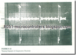
This loop has 28 T-states and eight operations (machine cycles). To execute the loop once, the microprocessor asserts the R̅D̅ signal seven times (the Opcode Fetch is also a Read operation) and the W̅R̅ signal once. Assuming the system clock frequency is 2 MHz, the loop is executed in 14 µS, and the WR signal, repeated every 14µS, can be observed on a scope. If we sync the scope on the W̅R̅ pulse from the Z80, we can check the output of the 8-input NAND gate (I̅O̅A̅D̅R̅), I̅O̅W̅R̅, and I̅O̅S̅E̅L̅ signals; W̅R̅ and I̅O̅S̅E̅L̅ signals of a working circuit are shown in Figure 5.12.

When the Z80 asserts the W̅R̅ signal, the port address 07H must be on the address bus A7-Ao, and the output of the NAND gate must be low. Similarly, the I̅O̅W̅R̅ must be low, and the IOSEL must be high. Now if we check the data bus in relation to the WR signal, one line at a time, we must read the data byte 97H.


5.7 ADDITIONAL ILLUSTRATIVE EXAMPLES: INTERFACING SENSORS AND MOTORS

5.7 ADDITIONAL ILLUSTRATIVE EXAMPLES:

INTERFACING SENSORS AND MOTORS

In previous examples, we illustrated the interfacing of I/O devices that were pri­marily binary devices (on/off). We now extend the concepts to interface analog devices such as temperature sensors and motors. In interfacing analog devices, the basic procedure remains similar to that of interfacing binary devices; the MPU identifies the device through a binary port address and enables it with an appro­priate control signal. However, we need to find a way to detect and to convert the analog signal into the binary format and vice versa. The analog signal is generally handled in two ways: one is to detect the signal when it reaches a predetermined level, and the other is to convert it into binary format proportional to its magni­tude. The predetermined level of the analog signal can be detected by using a comparator circuit, and the binary equivalent can be obtained by using an AID (Analog-to-Digital) data converter. In this section, we will focus on interfacing cir­cuits that can detect the predetermined level of analog signals and defer the dis­cussion of interfacing data converters to Chapter 13.

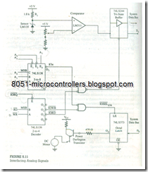
Figure 5.11 shows the interfacing of a temperature sensor. This circuit is designed to detect (through an input port) whether the temperature has risen to 100°C, and at that temperature it turns on the dc motor of a water pump. The de motor is interfaced with the MPU through an output port.

5.7.1 Hardware: Temperature Sensor LM135

And Comparator LM311

Figure 5.1l shows the LM 135 used as a temperature sensor. Its output is con­nected as one of the inputs to the comparator LM311. The LM135 is an integrated circuit, designed to sense changes in temperature; its output voltage changes 10 m V/ °C. It is rated to operate over a temperature range from – 55°C to + 150°C, and the current range 400 µA to 5 mA . At 25°C, the output of the sensor is typi­cally 2.98 V, and it increases I0mV/°C; therefore, at 100°C, it can reach 3.73 V (2.98 V + 750 mV).

z80 Interfacing and programming-21_03

The LM311 is a voltage comparator that can be operated from a + 5 V power Supply. The comparator compares two voltages at its input terminals, and if the difference between the two voltages is less than or equal to – 10 m V, its output remains at the saturation voltage of about 0.75 V; otherwise, the output is near the power supply voltage.

The output of the sensor is connected to the positive terminal of the com­parator, and its negative terminal is set to 3.73 V. At temperatures lower than 100°C the output voltage of the sensor is less than 3.73 V; thus, the comparator output remains at 0.75 V (logic 0). When the temperature reaches 100°C, the out­put of the sensor is 3.73 V, and the comparator output goes to + 4.5 V (logic I). The output of the comparator is connected to the tri-state buffer 74LS244, which serves as an input port to the MPU.

5.7.2 Interfacing Circuit for the Sensor

Figure 5.11 shows that the 74LS138 (3-to-8) decoder is used for address decoding. This decoding circuit is identical to the circuit shown in Figure 5.8; thus, the outputs of the decoder are asserted for port addresses ranging froin80H to87H ("don’t care" lines are assumed to be at logic 0). The control signals I̅O̅R̅D̅ (I/O’ Read) and I̅O̅W̅R̅ (I/O Write) are generated by using the 74LS139 (2-to-4) decoder; which is enabled by the I̅O̅R̅Q̅ signal. When the MPU intends to read, it asserts the I̅O̅R̅Q̅ and R̅D̅ signals. The input of the 2-to-4 decoder becomes 0 1, and the output O. goes active low to assert the IORD (I/O Read) control signal. The I̅O̅R̅D̅ is logically ANDed with the decoded address 80H to generate the I̅O̅S̅E̅L̅80H(I/O Select) signal, which enables the input buffer 74LS244 to read the output of the comparator. The output voltage of the comparator is connected to the data line Do through the buffer, and the MPU can monitor the temperature by monitoring the data line D0 .

5.7.3 Interfacing Circuit for the DC Motor

The de motor is interfaced with the MPU through the latch 74LS373; the output bit O0 of the latch can drive the de motor by turning on the transistor (Darlington pair). The logic level of bit O0 of the latch is controlled by the data line D0. The port address of the latch (87 H) is determined by the 3-to-8 decoder; the output line O7 of the decoder is ANDed with the control signal I̅O̅W̅R̅ to generate the IOSEL87H, which enables the latch 74LS373. When the temperature reaches 100°C, the MPU sends logic I to the latch (port 87H) to turn on the motor, and when the temperature is less than 100°C, the motor is turned off by the logic 0.

z80 Interfacing and programming-22_03

5.7.5 Program and Circuit Description

The first instruction IN A, (80H) enables the buffer 74LS244, reads the entire data bus D7, D0, and places the byte in the accumulator. However, we are interested in the logic level of only bit Do; it has the output of the comparator. Therefore, the next instruction ANDs the contents of the accumulator with the byte 01 H in order to eliminate bits D1-D6 and save the logic level of bit D0. When the temperature exceeds 100°C, the output of the comparator is about + 5 V, and the MPU reads logic 1 on the data line D0. When the temperature is lower than 100°C, the com­parator output is about 0.7 V, and the MPU reads logic 0 on the data line D; The next instruction OUT turns on the transistor if D0 = 1 or turns off the transistor if D0 = 0. When the transistor is on, it supplies the necessary current for the motor to run, and when the transistor is off. The motor is turned off. The last instruction JP takes the program back to the beginning and continuously monitors the changes in the output of the comparator.

5.7.6 Additional Sensors and Output Devices

Figure 5. 11 illustrates one example of interfacing a sensor and driving a dc motor. We can extend the same concepts to other sensing and output devices. In Figure 5. 11, we used only one data line Do to monitor the output of the comparator. We can connect additional sensors such as light detectors, level detectors, and smoke detectors to the remaining data lines and instructions can monitor all the sensors in a sequence. Similarly, we can connect output devices such as speakers, alarms, and lights by using solid state relays to the remaining output lines of the latch.


ILLUSTRATIVE EXAMPLE 3: APPLIANCE CONTROL USING MEMORY-MAPPED I/O TECHNIQUE

ILLUSTRATIVE EXAMPLE 3: APPLIANCE CONTROL USING MEMORY-MAPPED I/O TECHNIQUE

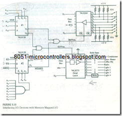
Figure 5.10 shows a schematic of interfacing I/O devices using the memory ­mapped I/O technique. The circuit includes one input port with eight DIP switches and one output port to control the appliances. The appliances are turned on and off by the microprocessor according to the corresponding switch positions. For example, the switch S7 controls the air conditioner and the switch S0 controls Light 4. All switch inputs are tied high; therefore, when a switch is open (off), it has + 5 V, and when a switch is closed (on), it has logic 0. The circuit includes two 3-to-8 decoders and one 8-input NAND gate to decode the address bus and generate the control signals. The eight switches are interfaced using a tri-state buffer 74LS244, and the appliances are interfaced using an octal latch (74LS373) with tri-state output.

5.6.1 Control Signals

In a memory-mapped I/O circuit, the control signals required are M̅R̅E̅Q̅ (Memory Request) and Read (R̅D̅) or Write (W̅R̅).In this circuit (Figure 5.10), they are used as inputs to a 3-to-8 decoder (labelled #2) to generate additional control signals. The enable lines of the decoder are controlled by the address lines. Assuming the
z80 Interfacing and programming-18_03
decoder is enabled by the appropriate address, we need to analyze the input and identify the output lines of the decoder that can be used as control signals.
To assert the Memory Write (M̅E̅M̅W̅R̅) signal, the input should be M̅R̅E̅Q̅= 0, W̅R̅= 0, and R̅D̅= 1 (R̅D̅ and WR cannot be active at the same time). With this input, the output line O4. goes active and generates the MEMWR signal.
To assert the Memory Read (M̅E̅M̅R̅D̅) signal, the input should be M̅R̅E̅Q̅= 0, W̅R̅ = 1, and R̅D̅ = 0. With this input to the decoder, the output O2 goes active and generates the M̅E̅M̅R̅D̅ signal.

5.6.2 Output Port and Its Address

The appliances are connected to the data bus through the latch 74LS373 and solid state relays. If an output bit of the 74LS373 is high, it activates the corresponding relay and turns on the appliance, which remains on as long as the bit stays high. Therefore, to control the appliances, we need to supply the appropriate bit pattern to the latch.
Figure 5.10 shows that the O̅E̅ of the latch is connected to the ground; thus, the latched data will keep the relays on or off according to the bit pattern. The LE is connected to the I/O select pulse, which is asserted when the output 00 of decoder #1 and the control signal M̅E̅M̅W̅R̅ go low. Therefore, to assert the I/O select pulse, the output port address should be 82FFH
z80 Interfacing and programming-19_03

5.6.3 Input Port and Its Address

The DIP switches are interfaced with the Z80 using the tri-state buffer 74LS244. The switches are tied high and are turned on by grounding shown in Figure 5.10. The switch positions can be read by enabling the signal O̅E̅ (O̅E̅1 and O̅E̅2), which is asserted when both the output O1 Of decoder #1 and the control signal M̅E̅M̅R̅D̅ go low. Therefore, to read the input port, the port address should be 86FFH
z80 Interfacing and programming-19_07

5.6.4 Instructions

To control the appliances according to switch positions, the microprocessor should read the bit pattern at the input port and send that bit pattern to the output port. The following instructions can accomplish this task. 

When this program is executed, the first instruction reads the bit pattern 1 0 1 1 0 111 (B7H) at the input port 86FFH and places that reading in the accumulator; this bit pattern represents the “on” position of switches S6 and S3 The second instruction complements the reading; this instruction is necessary because the “on” position has logic 0, and logic 1 is necessary to turn on solid state relays. The third instruction sends the complemented accumulator contents (0 I 00 I 000 = 48H) to the output port 82FFH. The 74LS373 latches the data byte 0 1 0 0 1 0 0 0 and turns on the space heater and Light 1. The last instruction, JP READ, takes the program back to the beginning and repeats the loop contin­uously in order to monitor the switches.
 

5.5 MEMORY-MAPPED I/O

5.5 MEMORY-MAPPED I/O

In, memory-mapped I/O, the input and output devices are assigned and identified by 16-bit addresses. To transfer data between the microprocessor and I/O devices, memory- related instructions (such as LD A, (16-bit) and memory control signals (such as M̅R̅E̅Q̅) are used. The microprocessor communicates with an I/O device as if it were one of the memory locations.

5.5.1 Memory-Related Data Transfer Instructions

To understand the memory-mapped I/O technique, we need to examine how a data byte is transferred from the Z80 to a memory location or vice versa. For example, the following instruction will transfer (copy) the contents of the accu­mulator to the memory location 8000H• It is assumed here that the instruction is stored in memory locations 2050H, 51H, and 52H

z80 Interfacing and programming-15_07

This is a 3-byte instruction; the first byte is the opcode, and the second and the third bytes specify the memory address. However, the 16-bit address 8000H is entered in the reverse order; the low-order byte 00 is stored in location 2051, followed by the high-order address 80H (the reason for the reversed order will be explained in section 5.9).In this example, if an output device instead of a memory register is connected at this address, the accumulator contents will be transferred to the output device. This is called the memory-mapped I/O technique.

Similarly, the instruction LD A, (4000H) will transfer the contents of the memory location 4000H to the accumulator. To assign this address for a memory ­mapped input port, we can interface an input device (for example a keyboard) instead of memory by using the memory-related control signals (MREQ and RD). When the processor executes the instruction, the accumulator receives data from the input device rather than from a memory register 4000H

5.5.2 Execution of Memory-Related Data Transfer Instructions

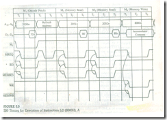
The execution of memory-related instructions discussed in the previous section is similar to the execution of I/O instructions (Sections 5.1 and 5.3), except that the memory-related instructions have 16-bit addresses. Figure 5.9 shows the execution of the instruction LD (8000H), A. It has four

Untitled-16_03

machine cycles; in the first three machine cycles, the Z80 reads the three bytes. The fourth machine cycle M4 (Memory Write) is similar to the machine cycle M3 of the OUT instruction. In this machine cycle, the Z80 places the 16-bit address 8000H on the address bus and the accumulator contents on the data bus. This is followed by the assertion of the control signals M̅R̅E̅Q̅ and W̅R̅ .The information available during M4 can be used to interface a memory-mapped output port with the 16-bit address 8000H

In memory-mapped I/O, I/O selection and data transfer require steps similar to those required in peripheral-mapped I/O:

1. Decode the entire address bus A15-A0 (rather than just A7-A0 )

2. Combine the control signals M̅R̅E̅Q̅, W̅R̅, and the decoded pulse from Step 1 to generate a pulse similar to the M̅S̅E̅L̅ pulse, which will be used to select an I/O rather than memory.

3. Use the I/O select pulse (actually M̅S̅E̅L̅) to enable the I/O port.

To interface a memory-mapped input port, the steps are similar to those of the memory-mapped output port. We can use the instruction LD A, (16-bit), which reads data from an input port with the 16-bit address and places it in the accumulator. The instruction has four machine cycles; only the fourth machine cycle differs from M4 in Figure 5.9. The control signal will be R̅D̅ rather than W̅R̅, and data flow from the input port to the microprocessor.