Effectively Optimizing Combinatorial:Boolean Arithmetic Laws and Optimizing for Technology

Boolean Arithmetic Laws

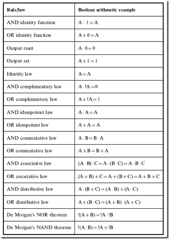
One of the ways of optimizing circuits is look through their output equations and try to find relationships that you can take advantage of using the rules and laws in Table 2-7. These rules should be committed to memory as quickly as possible (or at least written down on a crib sheet) to help you with

Table 2-7 Boolean arithmetic laws and rules.

image

optimizing logic equations without the need of truth tables or Karnaugh maps. Many of these rules and laws will seem self-evident, but when you are working at optimizing a logic equation in an exam, it is amazing what you will forget or won’t seem that obvious to you.

When I talk about using the laws and rules in Table 2-7 to simplify a logic equation, I normally use the term ‘‘reduce’’ instead of ‘‘optimize’’. The reason for thinking of these operations as a reduction is due to how much the logic equation shrinks as you work through it, trying to find the most efficient sum of products expression.

The two identity functions are used to indicate the conditions where an input value can pass unchanged through an AND or OR gate. The output set, reset and complementary laws are used to output a specific state when a value is passing through an AND or OR gate. The idempotent laws can be summarized by saying that if an input passes through a non-inverting gate, its value is not changed.

The remaining laws – commutative, associative and distributive – and De Morgan’s theorems are not as trivial and are extremely powerful tools when you have a logic equation to optimize. The commutative laws state that the inputs to AND and OR gates can be reversed, which may seem obvious, but when you have a long logic equation that is written in an arbitrary format (not necessarily in sum of product format), you can get confused very easily as to what is happening. It’s useful to have a law like this in your back pocket to change the logic equation into something that you can more easily manipulate.

To demonstrate the operation of these laws, we can go back to some of the logic circuits described in the Karnaugh map examples of the previous section. Looking at Fig. 2-3, the initial sum of products logic equation would be:

image

Using the AND associative law, I can rewrite this equation with the A term separate from the B and C terms to see if there are any cases where the B and C terms are identical.

imageBy doing this, I can see that the inside terms of the first and third products are identical. Along with this, I can see that the second and fifth products

are also identical. Using the OR distributive law, I can combine the first and third terms like:

image

Using the OR complementary law, I know that A OR !A will always be true. This is actually a clear and graphic example of the ‘‘don’t care’’ bit; regardless of the value of this bit, the output will be true so it can be ignored. The partial equation of the two terms reduces to:

image

The 1 ANDed with !B AND C can be further reduced using the AND identity law (1 AND A equals A):

image

This can be repeated for the second and fifth terms:

image

If you go back to the original logic equation, you will see that the fourth term (A · B · C) has not been reduced by combining it with another term. It can actually be paired with the third term (A · !B · C) by rearranging the two terms (using the AND commutative law) so that part of the terms operating on two bits are in common (A · C). Once this is done, the third and fourth terms can be reduced as:

image

After doing this work, the optimized or reduced sum of product logic equation for this function is

image

which is identical to what was found using the Karnaugh map.

Looking at the reduced logic equation, you should have noticed that there are two terms that will output a ‘‘1’’ at the same time ((!B · C) and (A · C) with A ¼ 1, B ¼ 0 and C ¼ 1). This is not a problem because the OR gate (even though the symbol that I use is a ‘‘þ’’) will only output a 1, regardless of how many true inputs it has. This was mentioned when the

Karnaugh maps were presented, but I wanted to reinforce that the same issue is present when you are reducing logic equations.

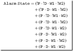
Before moving on, let’s go back to the home alarm logic equation and see if it can be reduced in the same way as the example above. Starting with the sum of products logic equation:

image

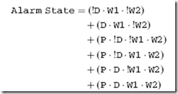
We can bring out the ‘‘P’’ values from the products and look for similarities in the remaining bracketed values and combine them using the associative, distributive, complementary and AND identity laws. I can see that the first and fourth, second and seventh can be combined, resulting in the logic equation:

image

Bringing ‘‘W1’’ to the forefront allows the combination of the third and fourth and fifth and sixth terms of the logic equation above, resulting in the new equation:

image

We have eliminated half the terms and, of those remaining, they are 25% smaller. Looking at the new logic equation, we can see that by combining the first and second terms (making ‘‘D’’ a don’t care bit in the process)

image

and combining the third and fourth terms (‘‘D’’ again is the don’t care bit) we end up with:

image

which is, again, the logic equation found by optimizing the function using truth tables or Karnaugh maps.

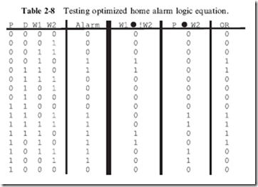
Personally, I tend to optimize logic equations using the Boolean arithmetic laws and rules listed in Table 2-7. Once a reduced sum of products equation has been produced, I then go back and compare its outputs in a truth table with the required outputs. In doing this, I present the values for each product (AND) and the final sum (OR) in separate columns, as shown in Table 2-8.

Optimizing for Technology

If you review the laws in Table 2-7 and correlate them to the text in the previous section, you’ll see that I missed the last two (De Morgan’s theorem). These two laws are not typically used during basic logic equation reduction because they typically involve converting part of an equation into an NAND or NOR gate, which is important when finally implementing a logic function in actual electronics. Another important aspect of optimizing for technology is adding functions out of the leftover gates in your circuit; by looking at how differently a logic circuit could be implemented, you may be able to add functionality to your circuit, without adding any cost to it.

image

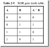
So far in the book, I haven’t discussed the ‘‘Exclusive OR’’ (XOR) gate in a lot of detail, but it is vital for implementing binary adders, as I will show you later in the book. In the first chapter, I presented the XOR gate with the truth table shown in Table 2-9.

You should probably be able to create the logic equation for the XOR

table as:

image

which does not seem like a very likely candidate for optimization. Similarly, you probably would have a hard time believing that the following logic equation would perform the same function:

image

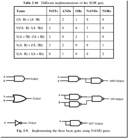
But, using De Morgan’s theorem as well as the other rules and laws from Table 2-7, I can go through the manipulations shown in Table 2-10 to show that they are equal, as well as count out the gates required by intermediate steps to give you a list of different implementations of the XOR gate. Each intermediate step in Table 2-10 is an implementation of the XOR gate that you could implement using the number of gates listed to the right of the terms.

It’s interesting to note that a total of five gates is required for each

implementation – this is not something that you can count on when you are

working at optimizing a circuit.

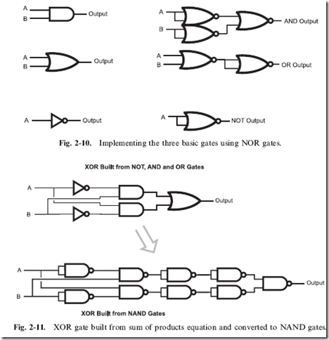
The basic gate used in TTL is the ‘‘NAND’’ gate: this means that the three

basic gates (AND, OR and NOT) are built from multiples of it, as I’ve shown

in Fig. 2-9. The basic gate for CMOS is the NOR gate, and Fig. 2-10 shows

how the three basic gates are implemented for it. The three gate NAND and

NOR equivalencies for the OR and AND gates, respectively, are perfect

examples of De Morgan’s theorem in operation. These implementations

image

can be checked against De Morgan’s theorem and the rules and laws presented in Table 2-7.

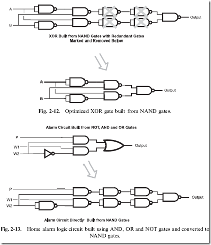
By understanding how gates are implemented in chips, we can now look at how to optimize the gates to provide the fastest possible operation of the logic function. Using the example of the XOR gate, we can graphically show how the gate is implemented using ANDs, ORs and NOTs and how these gates are implemented as NAND gates in TTL chips (Fig. 2-11).

Looking at the bottom logic diagram of Fig. 2-11, you can see that there are two sets of NAND gates wired as inverters together. Going back to Table 2-7, we can see that a doubly inverted signal is the same signal, so we can eliminate these two sets of NOT gates, as shown in Fig. 2-12. The resulting XOR circuit will pass signals through three NAND gates, which

image

counts as three ‘‘gate delays’’. This is an example of what I call ‘‘technology optimization’’: the logic circuit has been reduced to its bare minimum, taking advantage of the operation of the basic logic gates that make up the technology that it is implemented in.

Before moving on, I want to take one more look at the home alarm circuit that has been discussed throughout this chapter. I made a pretty bold statement at the start of the chapter, saying that it could be reduced to fit into the most basic TTL chip available – let’s see how honest I was being.

The (repeatedly) optimized logic equation for the home alarm system was:

image

image

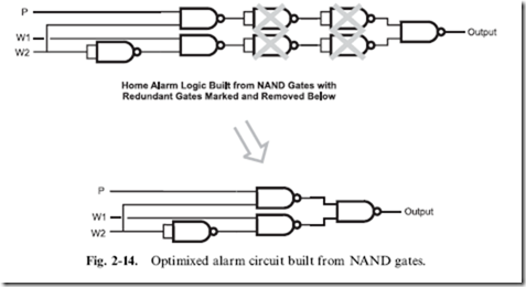
which could be first implemented in two AND, one OR and one NOT gate, as shown in Fig. 2-13 and converted to just NAND gates. You may have noted in Fig. 2-13 the remarkable similarity between the home alarm logic diagram and the XOR logic diagram – as I’ve shown in Fig. 2-14, the logic function reduces to just four NAND gates (one less than the XOR gate built out of NAND gates).

The final home alarm logic function requires four two input NAND gates – which is just what the 7400, the most basic TTL chip, provides. Every TTL chip, except for this one and a derivative revision, has more than four

image

gates built into them because they provide additional functions requiring multiple NAND gates. I was not exaggerating when I said that the home alarm logic function could be reduced to the most basic TTL chip available. In the next chapter, I will introduce you to the operation of TTL chips that provide the basis for digital electronic logic functions.

Quiz

1. The three parameters that are used to measure the optimization of a digital electronic circuit are:

(a) Cost, speed and complexity

(b) Gate delay, gate count and technology optimization

(c) Gate count, number of gate delays a signal must pass through and technology optimization

(d) Gate count, number of connections a signal must pass through and technology optimization

2. If TTL logic has a gate delay of 8 ns and the signal passing through an XOR gate built from NAND gates has to go through 9 gates and the shortest path is five gate delays, the time required for a signal to pass through the gates is:

(a) 40 ns

(b) 8 ns

(c) indeterminate

(d) 24 ns

3. When writing out a truth table, the inputs should be listed:

(a) Using a ‘‘Gray code’’

(b) Using a ‘‘binary progression’’

(c) In alphabetical order

(d) In order of importance

4. The ‘‘don’t care’’ bit in a truth table is:

(a) Indicated by a ‘‘dc’’ and replaces the common bits in two true sets of inputs

(b) Indicated by an ‘‘x’’ and replaces the common bits in two true sets of inputs

(c) Indicated by a ‘‘dc’’ and replaces the uncommon bits in two true sets of inputs

(d) Indicated by an ‘‘x’’ and replaces the uncommon bits in two true sets of inputs

5. When optimizing a logic function you can expect:

(a) That the number of chips that are required is reduced from the initial design

(b) That the optimized function runs faster than the initial design

(c) Cheaper chips can be used than in the initial design (d) Answers (a) through (c) are all possible and it might not be able to optimize the circuit from the initial sum of products equation

6. Karnaugh maps are:

(a) Tools designed to help you find your way around a digital electronic circuit

(b) A tool that will help you optimize a logic function

(c) The most efficient method of optimizing logic fuctions

(d) Hard to understand but must be used in every logic function design

7. The sum of products logic equation

image

can be reduced to:

(a) A · C

(b) !A · !B

(c) C · !B

(d) C

8. Which of the following pairs of Boolean arithmetic laws cannot be used together?

(a) Identity and De Morgan’s theorem

(b) Associative and idempotent

(c) Complementary and commutative

(d) All the laws and rules can be used together

9. The NAND equivalent to an AND gate is:

(a) Built from two NAND gates and requires two gate delays for a signal to pass through

(b) Built from three NAND gates and requires two gate delays for a signal to pass through

(c) Built from three NAND gates and requires three gate delays for a signal to pass through

(d) Built from one NAND gate as well as a NOT gate and requires two gate delays for a signal to pass through

10. Technology optimization is defined as:

(a) Designing the circuit which uses the fewest number of chips and signals pass through it as fast as possible

(b) Implementing logic functions to take advantage of the base logic of the logic technology used as well as using any leftover gates

(c) Finding the most efficient digital electronic technology to use for the application

(d) Designing circuitry that dissipates the least amount of heat to perform a desired function


Effectively Optimizing Combinatorial:Circuits ,Truth Table Function Reduction and Karnaugh Maps

Effectively Optimizing Combinatorial Circuits

In the first chapter, I introduced you to the basic theory behind digital electronics: binary data is manipulated by six different simple operations. With this knowledge, you actually have enough information to be able to design very complex operations, taking a number of different bits as input. The problem with these circuits is that they will probably not be ‘‘optimized’’ in order to minimize the number of gates, the speed which the digital electronic circuit responds to the inputs and finally, whether or not the circuit is optimized for the technology that it will be implemented in.

These three parameters are the basic measurements used to determine whether or not a circuit is effectively optimized. The number of gates should be an obvious one and you should realize that the more gates, the higher the chip count and cost of implementing the circuit as well as the increased complexity in wiring it. Right now, connections between logic gates are just black lines on paper to you – but when you start trying to wire circuits that you have designed, you will discover first hand that simplifying the wiring of a circuit often reduces costs more than reducing the number of chips would indicate. Small improvements in the complexity of a circuit can have surprising cost ramifications when you look at the overall cost of the application. You may find that eliminating 1% of the gates in an application will result in as much as a 10–20% overall reductions in product cost. These savings are a result of being able to build the circuit on a smaller PCB or one which requires fewer layers (which can reduce the overall product cost dramatically). If the application is going to use a programmable logic technology, you may find that with the optimized circuit, lower cost chips can be substituted into the design. Fewer gates in an application also results in less power being dissipated by the circuit, requiring less cooling and a smaller power supply.

The speed that signals pass through gates is not infinite; standard TTL requires 8 billionths of a second (called a ‘‘nanosecond’’ and uses the abbreviation ‘‘ns’’) to pass a signal through a ‘‘NAND’’ gate. The term given to this time is known as the ‘‘gate delay’’. Halving the number of gates a signal has to pass through (which is halving the number of gate delays) will double the speed in which it can respond to a changing input. As you work with more complex circuits, you will discover that you will often have to optimize a circuit for speed or else you may have to use a faster (and generally more expensive) technology.

The last parameter, what I call ‘‘technology optimization’’, on the surface may seem more intangible than the other two parameters as well as have its measurements use the other two parameters, but when working with physical devices, it is the most important factor in properly optimizing your application. Before moving on and considering your circuit ‘‘done’’, you should look at how it will actually be implemented in the technology that you are using and look for optimizations that will reduce the actual number of gates and gate delays required by the application.

You can consider logic optimization to be a recursive operation, repeatedly optimizing all the different parameters and measurements. Once you have specified the required logic functions, you should look at how it will be implemented in the actual circuit. Once you have converted it to the actual circuit, you will then go back and look for opportunities for decreasing the number of gates, speeding up the time the signal passes through the gates and again look for technology optimizations. This will continue until you are satisfied with the final result.

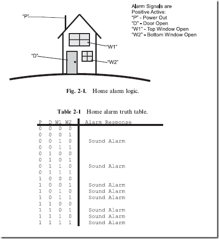
To illustrate what I mean, in this chapter, I will look at a practical example, a simple home burglar alarm. In Fig. 2-1, I have drawn a very basic house, which has two windows, a door and power running to it. Sensors, on

image

the windows, door and power are passed to an alarm system. When the alarm system was designed a table of the different possible combinations of inputs was generated (Table 2-1), with the combinations that would cause the alarm to sound indicated. As I have noted in Fig. 2-1, the alarm inputs are positive active, which means I can represent them as being active with a ‘‘1’’.

In this fictional house, I assumed that the upper window (‘‘W1’’) should never be opened – if it were opened, then the alarm would sound. Along with this, I decided that if the power failed and either of the windows were opened, then the alarm failed; this would be the case where the power to the house was cut and somebody forced open the window. Table 2-1 shows the cases where the alarm should sound and you will notice that the cases where the alarm should sound are either a single event in the table, or a case where three are grouped together.

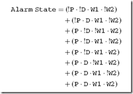
After building the table, you should also create a sum of products equation for the function:

image

You could also draw a logic diagram using the gate symbols that I introduced in the first chapter. I found that this diagram was very complex and very difficult to follow. If you were to try it yourself, you would discover that the logic diagram would consist of 12 NOTs, 24 two input ANDs (knowing that a single four input AND can be produced from three two input ANDs) and seven two input OR gates with the maximum gate delay being eleven (the number of basic TTL gates the signal has to pass through). At first take, this alarm function is quite complex.

Looking at Table 2-1 and the sum of products equation, you will be hard pressed to believe that this home alarm circuit can be significantly optimized, but in this chapter, I will show how these four alarm inputs and eight alarm events can be reduced to fit in the most basic TTL chip there is.

Truth Table Function Reduction

I like to tell new circuit designers to approach optimizing a logic circuit by first looking for opportunities in its truth table. This may not seem like a useful tool (especially in light of Table 2-1), but it can be as effective a tool as any of the others presented in this chapter. It can also be used as a useful verification tool for making sure that an optimized logic circuit will perform the desired function. The drawback to the truth table function reduction is that it tends to be the most demanding in terms of the amount of rote effort that you will have to put into it.

image

In the introduction to this chapter, the initial truth table I came up with didn’t seem very helpful. The reason for this is something that I will harp upon throughout this book – listing logic responses to binary input is not very effective, because of the large number of states that can change at any given time. If you look at Table 2-1, you will see that going from the state where P ¼ 0, D ¼ W1 ¼ W2 ¼ 1 to P ¼ 1, D ¼ W1 ¼ W2 ¼ 0 involves the changing of four bits. While this is a natural progression of binary numbers and probably an intuitive way of coming up with a number of different input states, it is not an effective way to look at how a logic circuit responds to varying inputs.

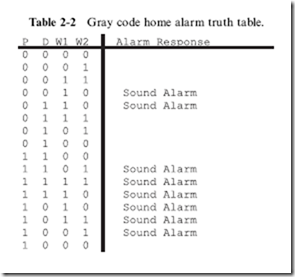
A much better method is to list the output responses in a truth table that is ordered using Gray codes, as I have shown in Table 2-2. Gray codes are a numbering system in which only one bit changes at a time: they are explained in detail along with how they are generated in Chapter 4. When you are listing data, regardless of the situation, you should always default to using Gray code inputs instead of incrementing binary inputs, as I have shown in Table 2-1.

Taking this advice, I recreated the home alarm system truth table using Gray codes in Table 2-2. When you look at Table 2-2, you should notice that the ‘‘discontinuities’’ of Table 2-1 have disappeared. The bit patterns which ‘‘Sound Alarm’’ group together quite nicely.

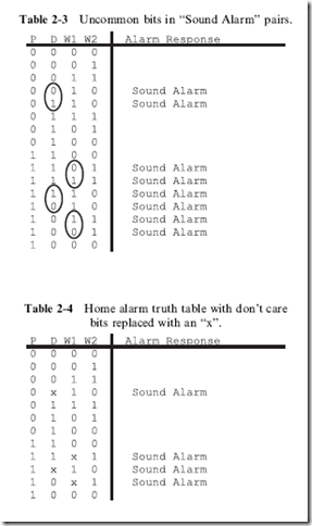
Looking at each value which ‘‘Sound Alarm’’, you’ll notice that each pair has three bits in common. To illustrate this, in Table 2-3, I have circled the bit which is different between each of the four pairs. In each of these

image

pairs, to sound the alarm we have very specific requirements for three bits, but the fourth bit can be in either state.

Another way of saying this is: for the alarm to sound, we don’t care what the fourth bit is and it can be ignored when we are determining the sum of products equation for the logic function. To indicate the ‘‘don’t care’’ bit, in Table 2-4, I have combined the bit pairs and changed the previously circled bits with an ‘‘x’’. This ‘‘x’’ indicates that the bit can be in either state for the output to be true. By replacing the two truth table entries with a single one with the don’t care bit indicated by an ‘‘x’’ you should see that something magical is starting to happen.

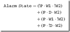
The obvious observation is that the table is shorter, but you should notice that the number of events which ‘‘Sound Alarm’’ has been halved and they are less complex than the eight original events. The sum of products equation for the bits shown in Table 2-4 is:

image

This sum of products expression will require four NOT gates, eight AND gates and three OR gates and the maximum gate delay will be nine. This has reduced the total gate count to less than 50% of the original total and this logic equation will operate somewhat faster than the original.

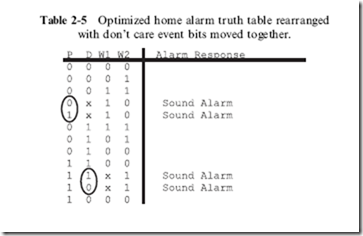
This is pretty good improvement in the logic circuit. You should be asking yourself if we can do better. To see if we can do better, I rearranged the data

in Table 2-4 so that the ‘‘Sound Alarm’’ events with common don’t care bits were put together and came up with Table 2-5. When I put the ‘‘Sound Alarm’’ events that had the same don’t care bits together, I noticed that in each of these cases, two of the remaining bits were in common and one bit changed in the two events (which I circled in Table 2.5). In Table 2-5, you may have noticed that the single changing bit of the original Gray code input sequence has been lost; this is not a problem. The Gray code sequence has served its purpose – it has indicated the initial input patterns which are common with its neighbors. In complex truth tables, you may have to rearrange bit patterns multiple times to find different

image


image

commonalities. When you do this, don’t worry about ‘‘loosing data’’; the important bit patterns are still saved in the active bit patterns.

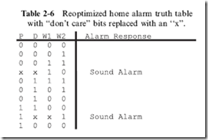
Table 2-6 shows what happens when the second don’t care bit is indicated. Since the two events which ‘‘Sound Alarm’’ do not have common don’t care bits, we can’t repeat this process any more. The two events from Table 2-6 can be written out as the sum of products:

image

This optimized ‘‘Alarm State’’ truth table has reduced our component count to one NOT gate, two AND gates and one OR gate and executes in five gate delays – quite an improvement from the original 43 gates and 11 gate delays!

Depending on how cynical you are, you might think that I ‘‘cooked up’’ this example to come up with such a dramatic improvement. Actually, the application shown here was my first attempt at coming up with a logic circuit to demonstrate how optimization operations of a logic circuit are performed; you will find similar improvements as this one when you start with a basic logic circuit and want to see how much you can reduce it.

Karnaugh Maps

Using truth tables is an effective but not very efficient method of optimizing digital logic circuits. A very clever French mathematician, Maurice Karnaugh (pronounced ‘‘carno’’) came up with a way to simplify the truth table optimization process by splitting the truth table inputs down the middle and arranging the two halves perpendicularly in order to display the relationships between bits more effectively. These modified truth tables are called ‘‘Karnaugh Maps’’ and are best suited for single bit output functions with three to six input bits.

My description of what a Karnaugh map is may sound cursory, but it is actually very accurate. A standard truth table can be considered to be a single dimensional presentation of a logic function and when it is properly manipulated, relationship between active outputs can be observed as I showed in the previous section. The problem with this method is that it is fairly labor intensive and will burn up a lot of paper. Karnaugh maps present the data in a two-dimensional ‘‘field’’ which allows for quick scanning of active output bits against their inputs, to find basic relationships between them.

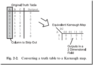
An example of converting a three input logic function from a truth table to a Karnaugh map is shown in Fig. 2-2. The initial logic function would be:

image

To create the Karnaugh map, I created a two by four matrix, with the rows being given the two different values for ‘‘A’’ and the columns given the four different values for ‘‘B’’ and ‘‘C’’. Note that the columns are listed as a two bit Gray code – this is an important feature of the Karnaugh map and, as I have pointed out, an important tool to being able to optimize a function. Once the two axes of the Karnaugh map are chosen, the outputs from the truth table are carefully transferred from the truth table to the Karnaugh map. When transferring the outputs, treat the Karnaugh map as a two-dimensional array, with the ‘‘X’’ dimension being the inputs which

image

weren’t stripped out and the ‘‘Y’’ dimension being the inputs which were stripped out from the truth table. When you are first starting out, this will be an operation in which you will tend to make mistakes because it is unfamiliar to you. To make sure you understand the process, it is a good idea to go back and convert your Karnaugh map into a truth table and compare it to your original truth table.

When you have created the Karnaugh map for your function, it is a good idea to either photocopy it or write it out in pen before going on. I am suggesting this action because, just as you did with the truth table, you are going to circle outputs which have the same unchanging bit patterns. As you circle the outputs, chances are you are not going to see the most effective groups of bits to circle together, or you will find that you have made a mistake in circling the bits. A photocopy or list in ink will allow you to try again without having to redraw the Karnaugh map.

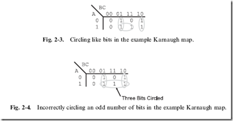
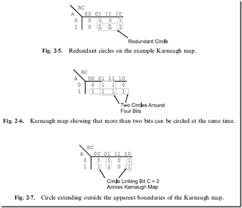
For the example shown in Fig. 2-2, the Karnaugh map has three circles put on it, as shown in Fig. 2-3. Each circle should result in combining two input sets together and making at least one bit into a ‘‘don’t care’’. Correctly circling bits can be difficult to understand, but there are a few rules that can be applied to it. First, each circle must be around a power of two number of bits – you cannot circle three bits (as shown in Fig. 2-4 for this example). Secondly, it is not a problem if circles overlap over specific bits. I should point out that there is the case for redundant circles (Fig. 2-5). If a circle is drawn and all the circled bits are enclosed in another circle, then the enclosed circle is redundant. Thirdly, remember that when you are circling bits that you want to circle a power of two number of bits, not just two. In Fig. 2-6, I have modified the three bit Karnaugh map with the outputs at A = 0 and B = C = 1 and A = 1 and B = C = 0 being a ‘‘1’’

image


image

and found that I could circle two groups of four bits. In each of these cases, I have made two bits ‘‘don’t care’’.

Finally, saying that a Karnaugh map is like a two-dimensional array is

inaccurate – it is actually a continuum unto itself, with the tops and sides being connected. When you draw out your Karnaugh map, you may find that the bits which can be circled (meaning ones with similar patterns) are on opposite ends of the Karnaugh map. This is not a problem as long as there are matching bits.

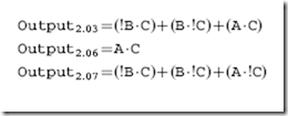
Once you have the outputs circled, you can now start writing out the optimized equation. As an exercise, you might want to look at the example Karnaugh maps in Figs. 2-3, 2-6 and 2-7. The output equations for these figures are:.

image


image

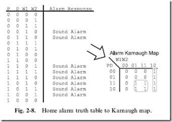
In this chapter, I wanted to show how the different optimizing tools are used for the home alarm system presented in the chapter introduction. The alarm system’s functions can be optimized using the Karnaugh map shown in Fig. 2-8. In Fig. 2-8, I have drawn the circles around the two groups of four active output bits which are in common and result in the logic equation

image

which is identical to the equation produced by the truth table reduction and a lot less work.

Before going on, I want to just say that once you are comfortable with Karnaugh maps, you will find them to be a fast and efficient method of optimizing simple logic functions. Becoming comfortable and being able to accurately convert the information from a truth table to a Karnaugh map will take some time, as will correctly circling active outputs to produce the optimized sum of products circuit. Once you have mastered this skill, you will find that you can go directly to the Karnaugh map from the requirements without the initial step of writing out the truth table.


The Underpinnings of Digital Electronics : Boolean Arithmetic, Truth Tables and Gates,The Six Elementary Logic Operations,Combinatorial Logic Circuits: Combining Logic Gates,Sum of Products and Product of Sums and Waveform Diagrams

The Underpinnings of Digital Electronics

If you were asked to define what a bit is, chances are you would probably do a pretty good job, saying something like:

A bit is something that can only have two values: on or off.

Instead of ‘‘on or off ’’, you might have used terms for two values like ‘‘one or zero’’, ‘‘high or low voltage’’, ‘‘up or down’’, ‘‘empty or full’’ or (if you fancy yourself as being erudite) ‘‘dominant or recessive’’. All of these terms are correct and imply that the two values are at opposite extremes and are easily differentiated.

When you think of ‘‘bits’’, you are probably thinking of something in a wire or an electronic device contained within a computer, but when the concept of binary (two state) logic was first invented, the values that were

applied were tests to see if a statement was ‘‘true’’ or ‘‘false’’. Examples of true and false statements are:

● The sun always rises in the East. (true)

● Dogs live at the bottom of the ocean like fish. (false)

Looking at these simple statements determining if they are true or false seems to reduce the information within to an extreme degree. The truthfulness of a statement can be combined with another statement to help determine if a more complex postulate is true. If you consider the following ‘‘true’’ statements:

● A dog has fur over its body.

● A dog has four legs.

● Animals have four legs and fur.

● Humans have two legs.

● A snake has scales on its body.

● A reptile’s body has scales or smooth skin.

and combining them together, you can make some surprisingly complex ‘‘assertions’’ from these data using three basic operations. These three basic operations consist of ‘‘AND’’ which is true if all the statements combined together by the AND are true, ‘‘OR’’ which is true if any of the combined statements are true and ‘‘NOT’’ which is true if a single statement is false. To differentiate these three operations from their prose synonyms, I will capitalize them (as well as other basic logic operations) throughout the book. These operations are often called ‘‘logic operations’’ because they were first used to understand the logic of complex philosophical statements.

From the seven statements above and using these three basic operations, you can make the following true assertions:

● Humans are not dogs.

● A dog is an animal.

● A snake is a reptile.

The first statement is true because we know that a human has two legs (violating a condition that is required for the definition of a dog to be true). This is an example of the ‘‘negation’’ or ‘‘NOT’’ operation; the assertion is true if the single input statement is false:

The room is dark because the lights are not on.

The NOT function is often called an ‘‘Inverter’’ because it changes the value of the input from high to low and vice versa.

The second assertion, ‘‘A dog is an animal’’, is true because both of the two statements concerning animals are true when applied to dogs (which have four legs and fur). This is an example of the ‘‘AND’’ operation; the assertion is true if and only if the input statements are true. The AND operation has two or more input statements. In trying to differentiate bicycles and motorcycles from cars, you might make the assertion which uses the AND operation:

A car has four wheels and a motor.

The last assertion, ‘‘A snake is a reptile’’, is true because one of the two statements giving the necessary characteristics for a reptile is true. This is an example of an ‘‘inclusive or’’ (usually referred to as just ‘‘OR’’) operation; the assertion is true if any of the input statements are true. Like the ‘‘and’’ operation, OR can have two or more input statements. If you’re a parent, you will be familiar with the assertion:

During the course of a day, a baby eats, sleeps, cries or poops.

I use this example to illustrate an important point about the ‘‘OR’’ operation that is often lost when it is used in colloquial speech: if more than one input statement is true, the entire assertion is still true. As incredible as it sounds to someone who has not had children yet, a baby is very capable of performing all four actions listed above simultaneously (and seemingly constantly).

I’m making this point because when we speak, we usually use the ‘‘exclusive or’’ instead of ‘‘inclusive or’’ to indicate that only one of two actions can be true. An example statement in which an ‘‘exclusive or’’ is used in everyday speech could be:

Tom is at a restaurant or the movies.

This is an example of ‘‘exclusive OR’’ because Tom can only be at one of the two places at any given time. I will discuss the ‘‘exclusive or’’ operation in more detail later in this chapter, but for now try to remember that an assertion using the ‘‘OR’’ operation will be true if one or more of the input statements are true.

So far I have been working with ‘‘bits’’ of ‘‘binary’’ information contained in ‘‘statements’’ and ‘‘assertions’’. You are probably wondering why a term like ‘‘bit electronics’’ or ‘‘binary electronics’’ is used instead of ‘‘digital electronics’’. ‘‘Digital’’ comes from the Latin word for ‘‘fingers’’ and indicates that there are many discrete signals that are at one of two values. Naming the circuitry ‘‘bit electronics’’ or ‘‘binary electronics’’ would imply that it can only work with one piece of information; digital electronic circuits

can process many bits of information simultaneously, either as separate pieces of information or collections of large amounts of data.

In the first few pages of this book, I have introduced you to the concept of the ‘‘bit’’, the ‘‘digit’’, the ‘‘NOT’’, ‘‘AND’’ and ‘‘OR’’ operations along with the ‘‘exclusive OR’’. Different combinations of these concepts are the basis for the majority of the material presented through the remainder of this book and any course in digital electronics. I suggest that you read over this chapter and make sure you are completely comfortable with the terms and how they work before going on.

Boolean Arithmetic, Truth Tables and Gates

In the introduction to this chapter, I demonstrated the operation of the three operations ‘‘AND’’, ‘‘OR’’ and ‘‘NOT’’, which can be used to test input values (which are in the form of two state ‘‘bits’’) and produce assertions based on the state of the input bits. The verbose method I used could be used with digital electronics, but you will find that it is cumbersome and not intuitively obvious when you are working with electronic circuits. Fortunately, a number of different tools have been developed to simplify working with logic operations.

The first tool that simplifies how logic operations are expressed is known as ‘‘Boolean arithmetic’’ (or sometimes as ‘‘Boolean logic’’), a branch of mathematics where a mathematical expression is used to express how bit inputs can be transformed into an output using the three operations presented in the introduction. Boolean arithmetic was first described by the English mathematician Charles Lutwidge Dodgson, whom you may be familiar with by his nom de plume Lewis Carroll, and expanded upon by George Boole, in the mid 19th century, as a way of understanding, proving or disproving complex philosophical statements. Boole demonstrated that a statement, involving bits of data and the AND, OR or NOT operations could be written in the form:

image

The braces (‘‘{‘‘ and ’’}’’) are often used to indicate that what’s inside them is optional and the three periods (‘‘.. .’’) indicate that the previous text can be repeated. Using these conventions you can see that a Boolean arithmetic statement is not limited to just one operation with two input bits – they can actually be very lengthy and complex with many bit inputs and multiple operations.

To demonstrate how a Boolean arithmetic statement could be articulated, I can write the proof that a dog is an animal in the form:

image

If both statements within the parentheses are true, then the ‘‘Result’’ will be true.

This method of writing out assertions and the logic behind them is quite a bit simpler and much easier to understand, but we can do better. Instead of writing out the true or false statement as a condition, it can be expressed in terms of a simple ‘‘variable’’ (like ‘‘X’’). So, if we assign ‘‘A’’ as the result of testing if dogs have four legs and ‘‘B’’ as the result of testing if dogs have fur, we can write out the Boolean arithmetic equation above as:

Result =A AND B

To further simplify how a logic operation is written out, the basic characters ‘‘.’’, ‘‘+’’ and ‘‘!’’ can be used instead of AND, OR and NOT, respectively. AND behaves like a binary multiplication, so along with the ‘‘.’’ character, you may see an ‘‘x’’ or ‘‘*’’. The OR operation may be represented as ‘‘|’’. The ampersand (‘‘&’’) for AND and ‘‘|’’ for OR are often used because they are the same symbols as are used in most computer programming languages. When I write out Boolean arithmetic equations throughout the book, I will be using the ‘‘.’’, ‘‘+’’ and ‘‘!’’ characters for the three basic logic operations instead of the full words.

An important advantage of converting a statement into a simple equation is that it more clearly shows how the logic operation works. If the variables ‘‘A’’ and ‘‘B’’ were just given the values of ‘‘true’’ or ‘‘false’’, the ‘‘Result’’ of the equation above could be written out in the form shown in Table 1-1. This is known as a ‘‘truth table’’ and it is a very effective way of expressing how a Boolean operator works. The truth table is not limited to just three inputs,

Table 1-1 ‘‘AND’’ operation truth table using Gray code inputs.

Input ‘‘A’’

Input ‘‘B’’

‘‘AND’’ Output

False

False

False

False

True

False

True

True

True

True

False

False

and a function with more than one Boolean operator can be modeled in this way. Functions with more than one output can be expressed using the truth table, but I don’t recommend doing this because relationships between inputs and outputs (which I will discuss in greater detail later in the book) can be obscured.

One other thing to notice about the truth table is that I have expressed the inputs as a ‘‘Gray code’’, rather than incrementing inputs. Gray codes are a technique for sequencing multiple bits in such a way that only one bit changes from one state to the next. Incrementing inputs behave as if the inputs were bits of a larger binary number and the value of this number is increased by one when moving from one state to the next. The truth table above, for the ‘‘AND’’ gate could be written out using incrementing inputs as Table 1-2.

In many cases, truth tables are introduced with incrementing inputs, but I would like to discourage this. Incrementing inputs can obscure relationships between inputs that become obvious when you use Gray codes. This advantage will become more obvious as you work through more complex logic operations and are looking for ways to simplify the expression.

The OR operation’s truth table is given in Table 1-3, while the NOT operation’s truth table is shown in Table 1-4.

The OR operation would be written in Boolean arithmetic, using the ‘‘þ’’ character to represent the OR operation as:

Output = A + B

and the NOT operation (using the ‘‘!’’ character) is written out in Boolean arithmetic as:

Output = !A

Table 1-2 ‘‘AND’’ operation truth table using incrementing inputs.

Input ‘‘A’’

Input ‘‘B’’

‘‘AND’’ Output

False

False

False

False

True

False

True

False

False

True

True

True

Table 1-3 ‘‘OR’’ operation truth table using Gray code inputs.

Input ‘‘A’’

Input ‘‘B’’

‘‘OR’’ Output

False

False

False

False

True

True

True

True

True

True

False

True

Table 1-4 ‘‘NOT’’ operation truth table using Gray code inputs.

Input

‘‘NOT’’ Output

False

True

True

False

Sometimes, when a signal is NOTted, its symbol is given either a minus sign (‘‘-‘‘) or an underscore (‘‘_’’) as its first character to indicate that it has been inverted by a NOT operation.

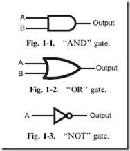
The final way of expressing the three basic logic operations is graphically with the inputs flowing through lines into a symbol representing each operation and the output flowing out of the line. Figures 1-1 through 1-3 show the graphical representations of the AND, OR and NOT gates, respectively.
image

The graphical representation of the logic operations is a very effective way of describing and documenting complex functions and is the most popular way of representing logic operations in digital electronic circuits. When graphics are used to represent the logic operations, they are most often referred to as ‘‘gates’’, because the TRUE is held back until its requirements are met, at which point it is allowed out by opening the gate. ‘‘Gate’’ is the term I will use most often when describing Boolean arithmetic operations in this book.

If you were to replace the lines leading to each gate with a wire and the symbol with an electronic circuit, you can transfer a Boolean arithmetic design to a digital electronic circuit directly.

The Six Elementary Logic Operations

When you look at a catalog of digital electronics chips, you are going to discover that they are built from ANDs, ORs and NOTs as well as three other elementary gates. Two of these gates are critically important to understand because they are actually the basis of digital logic while the third is required for adding numbers together.

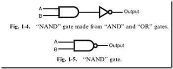
TTL logic is based on the ‘‘NAND’’ gate which can be considered a ‘‘NOTted AND’’ – the output of an AND gate is passed through a NOT gate as shown in Fig. 1-4. Instead of drawing the NAND gate as an AND gate and NOT gate connected together as in Fig. 1-4, they are contracted into the one symbol shown in Fig. 1-5. It’s truth table is in Table 1-5.

When writing out the NAND function in Boolean arithmetic, it is normally in the form:

image

which is a literal translation of the operation – the inputs are ANDed together and the result is NOTted before it is passed to the Output.
image

Table 1-5 ‘‘NAND’’ operation truth table.

Input ‘‘A’’

Input ‘‘B’’

‘‘NAND’’ Output

False

False

True

False

True

True

True

True

False

True

False

True

clip_image006Fig. 1-6 ‘‘NOR’’ gate.

You will see the small circuit on various parts in different electronic devices, both on inputs and outputs. The small circle on the NAND gate is the conventional shorthand symbol to indicate that the input or output of a gate is NOTted.

In case you didn’t note the point above, the NAND gate is the basis for TTL logic, as I will explain later in the book. Being very comfortable with NAND gates is very important to being able to design and use TTL electronics. This is a point that I find is not stressed enough in most electronics courses and by having a strong knowledge of how NAND gates

work as well as how they are implemented you will better understand what is happening within your digital electronics circuits. If you are going to be working with CMOS logic, in the same way you should be comfortable with the NAND gate for TTL, you should be familiar with the ‘‘NOR’’ gate (Fig. 1-6). The NOR gate ca  be considered to be a contraction of the OR and NOT gates (as evidenced by the circle on the output of the OR gate) and operates in the opposite manner as the OR gate, as shown in Table 1-6. When using NOR operations in Boolean arithmetic, a similar format to the NAND gate is used:

image

The last elementary logic gate that you will have to work with is the ‘‘Exclusive OR’’ (Fig. 1-7) with Table 1-7 being its truth table. The

Table 1-6 ‘‘NOR’’ operation truth table.

Input ‘‘A’’

Input ‘‘B’’

‘‘NAND’’ Output

False

False

True

False

True

False

True

True

False

True

False

False

clip_image007Fig. 1-7. ‘‘XOR’’ gate.

Table 1-7 ‘‘Exclusive OR’’ operation truth table.

Input ‘‘A’’

Input ‘‘B’’

‘‘Exclusive OR’’ Output

False

False

False

False

True

True

True

True

False

True

False

True

Exclusive OR (also referred to as ‘‘Ex-OR’’ or ‘‘XOR’’) only returns a True output if only one of its inputs is true. If both inputs are the same, then the Exclusive OR outputs False. The Boolean arithmetic symbol for Exclusive OR is often a caret (‘‘^’’) as is used in computer programming languages or a circle with an ‘‘x’’ character in it ®. Writing a Boolean statement with the Exclusive OR would be in the format:

Output = A ^ B

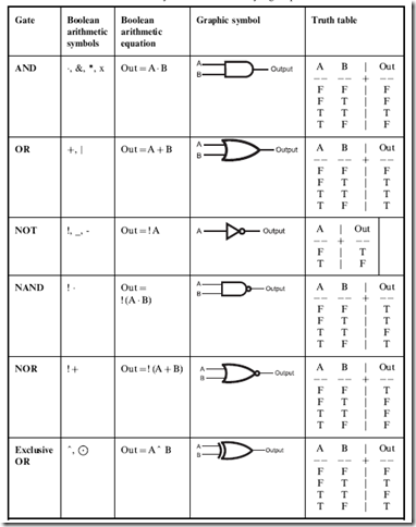
Table 1-8 summarizes the six elementary gates along with their Boolean arithmetic symbols and formats, graphical symbols and truth tables.

Table 1-8 Summary of the six elementary logic operations.
image

Combinatorial Logic Circuits: Combining Logic Gates

As I hinted at in the previous section, multiple gate functions can be combined to form more complex or different Boolean logic functions. Wiring together multiple gates are used to build a complex logic function that only outputs a specific value when a specific combination of True and False inputs are passed to it is known as ‘‘combinatorial logic’’. The output of a combinatorial logic circuit is dependent on its input; if the input changes then the output will change as well.

When I wrote the preceding paragraph, I originally noted that combinatorial logic circuits produce a ‘‘True’’ output for a given set of inputs. This is incorrect, as there will be some cases where you will require a False output in your application. I made the definition a bit more ambiguous so that you do not feel like the output has to be a single, specific value when the input consists of the required inputs. It is also important to note that in a combinatorial logic circuit, data flows in one direction and outputs in logic gates cannot be used as inputs to gates which output back to themselves. These two points may seem subtle now, but they are actually critically important to the definition of combinatorial logic circuits and using them in applications. An example of a combinatorial circuit is shown in Fig. 1-8. In this circuit, I have combined three AND gates, a NOR gate, a NOT gate and an XOR gate to produce the following logic function:

image

This combinatorial circuit follows the convention that inputs to a gate (or a chip or other electronic component) are passed into the left and outputs

image

Fig. 1-8 Combinatorial circuit built from multiple logic gates.

exit from the right. This will help you ‘‘read’’ the circuit from left to right, something that should be familiar to you.

While seeing a series of logic gates, like the one in Fig. 1-8, seems to be overwhelming, you already have the tools to be able to work through it and understand how it works. In the previous section, I noted that gates could be connected by passing the output of one into an input of another; a combinatorial circuit (like Fig. 1-8) is simply an extension of this concept and, being an extension, you can use the same tools you used to understand single gates to understand the multiple gate operation.

should point out that the two broken lines on the left side of Fig. 1-8 (leading down from ‘‘A’’ and ‘‘B’’) indicate that these lines are not connected to the lines that they intersect with. You will find that it can be very difficult to design logic circuits without connected and separate lines from becoming confused. In Fig. 1-9, I have shown a couple of the conventional ways of drawing intersecting lines, depending on whether or not they connect or bypass each other. Probably the most intuitively obvious way of drawing connecting and bypassing lines is to use the dot and arc, respectively. I tend not to because they add extra time to the logic (and circuit) diagram drawing process. As you see more circuit diagrams, you will see the different conventions used and you should be comfortable with recognizing what each means.

image_thumb[1]

Fig. 1-9. Different representations for wires that connect or bypass.

image_thumb[2]

Fig. 1-10. Combinatorial circuit with logic gate outputs marked.

When I am faced with a complex combinatorial circuit, the first thing I do is to mark the outputs of each of the gates (Fig. 1-10) and then list them according to their immediate inputs:

image_thumb[3]

After listing them, I then work through a truth table, passing the outputs of each gate along until I have the final outputs of the complete function (Table 1-9). In keeping with my comments of the previous section, I have used a three bit Gray code for the inputs to this circuit.

Before going on, there are two points that I would like you to keep in the back of your mind. First, this is actually quite an efficient methodology for decoding combinatorial circuits that you are given the design for. Designing a logic gate circuit that responds in a specific manner is actually quite a different process and I will be devoting the rest of this chapter as well as the next to explaining the design and optimization of combinatorial circuits. Once you have finished with Chapter 2, you might want to revisit the example circuit in Fig. 1-8 and see how effectively you can reduce its complexity and the number of logic gates needed to implement it. The second point that you should be aware of is the example circuit that I used in this section is actually quite unwieldy and does not conform to the typical methods used to design most practical combinatorial digital electronic circuits. In the next section, I will present you with the conventional methods for specifying and documenting combinatorial circuits.

Table 1-9 Decoding the response of the combinatorial circuit in Fig. 1-8.

image_thumb[4]

Sum of Products and Product of Sums

Presenting combinatorial circuits as a collection of gates wired together almost randomly, like the circuit shown in Fig. 1-8, is sub-optimal from a variety of perspectives. The first is, the function provided by the combinatorial circuit is not obvious. Secondly, using a variety of different gates can make your parts planning process difficult, with only one gate out of many available in a chip being used. Lastly, the arrangement of gates will be difficult for automated tools to combine on a printed circuit board (‘‘PCB’’) or within a logic chip. What is needed is a conventional way of drawing combinatorial logic circuits.

The most widely used format is known as ‘‘sum of products’’. Earlier in the chapter, I presented the concept that the AND operation was analogous to multiplication just as the OR operation is to addition. Using this background, you can assume that a ‘‘sum of products’’ circuit is built from AND and OR gates. Going further, you might also guess that the final output is the ‘‘OR’’ (because addition produces a ‘‘sum’’) with the gates that

image_thumb[5]

Fig. 1-11. Example ‘‘sum of products’’ combinatorial logic circuit.

convert the inputs being ‘‘AND’’ gates (a ‘‘product’’ is the result of a multiplication operation). An example ‘‘sum of products’’ combinatorial logic circuit is shown in Fig. 1-11.

In this circuit, the inputs are ANDed together and the result is passed to an OR gate. In this circuit, the output will be ‘‘True’’ if any of the inputs to the OR gate (which are the outputs from the AND gates) are true. In some cases, to make sure that the inputs and outputs of the AND gates are in the correct state, they will be inverted using NOT gates, as I have shown in Fig. 1-11.

Figure 1-11 has one feature that I have not introduced to you yet and that is the three input OR gate on the right side of the diagram. So far, I have only discussed two input gates, but I should point out that three input gates can be built from multiple two input gates, as I show in Fig. 1-12, in which two, two input AND gates are combined to form a single three input AND gate. A three input OR gate could be built exactly the same way.

A three input NAND or NOR gate is a bit trickier, as Fig. 1-13 shows. For this case, the output of the NAND gate processing ‘‘A’’ and ‘‘B’’ must be inverted (which can be accomplished with a NAND gate and both inputs tied together as I show in Fig. 1-13) to make its output the same as an ‘‘AND’’. The NAND gate’s function is to first AND its inputs together and then invert them before driving out the output signal. As I will explain in greater detail in the next chapter, an inverted output, when it is inverted, becomes a ‘‘positive’’ output and I use this rule to produce the three input NAND gate. A three input NOR gate would be built in exactly the same way as a three input NAND gate.

image_thumb[6]

Along with having a ‘‘sum of products’’ combinatorial logic circuit that outputs a True when one of the intermediate AND gates outputs True, there is the complementary ‘‘product of sums’’ (Fig. 1-14), which outputs False when one of its intermediate OR gates outputs False.

While product of sums combinatorial circuits can produce the same functions as sum of product combinatorial circuits, you will not see as many product of sum combinatorial circuits in various designs because they rely on what I call ‘‘negative logic’’. Most people cannot easily visualize something happening because the inputs do not meet an expected case, which is exactly what happens in a product of sums combinatorial logic circuit.

To demonstrate how a sum of product combinatorial logic circuit is designed, consider the messy combinatorial logic circuit I presented

image_thumb[7]

Fig. 1-14. Example ‘‘product of sums’’ combinatorial logic circuit.

in the previous section (see Fig. 1-8). To understand the operation of this circuit, I created a large truth table (Table 1-9) and listed the outputs of each of the intermediate gates and finally discovered that the function output True in three cases that can be directly translated into AND operations by assuming that in each case the output was true and the input conditions were all true. To make all three inputs True to the AND gates when the input is False, I invert them and came up with the three statements below:

A : B · !C

A · B · C

!A · B · !C

These three AND statements can be placed directly into a sum of products combinatorial circuit, as shown in Fig. 1-15.

Looking at Fig. 1-15, you’ll probably notice that this circuit has the same total number of gates as the original circuit – and, assuming that each three input gate is made up of two, two input AND gates, it probably requires four more gates than the original circuit shown in Fig. 1-8. The only apparent advantage to the sum of product format for combinatorial logic circuit is that it is easier to follow through and see that the output is True for the three input conditions I listed above.

In the following chapters, I will introduce you to combinatorial logic circuit optimization as well as explain in more detail how digital electronic gates are actually built. It will probably be surprising to discover that the sum

image_thumb[8]

of product combinatorial logic circuit format leads to applications that are more efficient (in terms of total gate or transistor count along with speed and heat dissipation) than ones using less conventional design methodologies.

Waveform Diagrams

So far in this chapter, I have shown how logic functions can be presented as English text, mathematical equations (Boolean arithmetic), truth tables and graphical circuit diagrams. There are actually two more ways in which the logic data can be presented that you should be familiar with. The first method is not one that you will see a lot of except when debugging microprocessor instructions from a very low level, while the second is one that you will have to become very familiar with, especially when the digital electronic signals pass from the combinatorial logic shown here to more complex circuits that have the ability to ‘‘store’’ information.

The first method, the ‘‘state list’’ consists of a list of text columns for each state of the circuit. The state list is really a compressed form of the truth table and is best suited for displaying a fairly large amount of numerical data. Going back to the example circuit of Fig. 1-8, and Table 1-9, I could express the truth table as the series of columns below. Note that I have used the numeric values ‘‘1’’ for True and ‘‘0’’ for False because they are easier to

differentiate than ‘‘T’’ and ‘‘F’’ over a number of rows.

image_thumb[9]

As I said, not a lot of information is obvious from the state list. Some format- ting could be done to make the inputs and outputs better differentiated, but for the most part, I don’t recommend using state lists for most digital electronics applications. Where the state list is useful is in debugging state machine or microcontroller applications in which you have added hardware to the data, address and control busses to record how the device responds to specific inputs.

The state list is not ideal for this type of application, but it’s better than nothing. The other method, which is not only recommended as a circuit analysis and design tool but is also one you should be intimately familiar with is the ‘‘waveform diagram’’. Waveforms are electrical signals that have been plotted over time. The original waveform display tool was the oscilloscope; a drawing of a typical oscilloscope’s display is shown in Fig. 1-16.

image_thumb[10]

The features of the two ‘‘waveforms’’ displayed on the oscilloscope screen can be measured by placing them against the ‘‘graticule markings’’ on the display. These markings (usually just referred to as ‘‘graticules’’ and etched onto the glass screen of the oscilloscope) are indicators of a specific passage of time or change in voltage. Along with the ‘‘gross’’ graticules, most oscilloscopes have finer markings, to allow more accurate measurements by moving the waveforms over them.

Oscilloscopes are very useful tools for a variety of different applications, which contain varying voltage levels (which are known as ‘‘analog’’ voltage levels). They can be (and often are) used for digital logic applications but they are often not the best tool because digital waveforms only have two levels, when applied to electronics: digital signals are either a high voltage or a low voltage. The timing of the changes of these two voltage levels is more interesting to the designer.

So instead of thinking of digital waveforms in terms of voltage over time, in digital electronics, we prefer to think of them as states (High/Low, True/ False, 1/0) over time and display them using a waveform diagram like the one shown in Fig. 1-17. When designing your digital electronics circuit, you will create a waveform diagram to help you understand how the logic states will be passed through the circuit; later, when you are debugging the circuit, you will be comparing what you actually see with this diagram to see if your assumptions about how the circuit would operate are correct. The different signals shown in Fig. 1-17 are samples of what you will see when you are designing your own application circuit.

image_thumb[11]

image_thumb[12]

The waveform diagram is the first tool that will help you optimize your circuit. Before writing up this section, I was planning on the diagrams I wanted to include with it and one was a waveform representation of the first example combinatorial logic circuit’s operation from Table 1-9. The thin vertical lines indicate the edges of each state.

After drawing out Fig. 1-18, it was obvious that signals ‘‘1’’ and ‘‘4’’ (from the marked circuit diagram Fig. 1-8) were redundant. Looking back at the diagram for the circuit, I realized that the AND gate with output 4 and inverter with output 3 could be completely eliminated from the circuit – the output of AND gate 1 could be passed directly to the XOR gate (with output 6).

The waveform diagram shown in Fig. 1-18 is what I call an ‘‘idealized waveform diagram’’ and does not encompass what is actually happening in a physical circuit. Looking at Fig. 1-18, you will see that I have assumed that the switching time for the gates is instantaneous. In real components, switching time is finite, measurable and can have a significant impact to your application’s ability to work. This is discussed in more detail in later chapters. Finally, this circuit does not allow for basic errors in understanding, such as

what happens when multiple gate outputs are passed to a single gate input – your assumption of this type of case may not match what really happens in an actual circuit.

In this chapter, I have introduced you to the basic concepts of combinatorial logic circuits and the parts that make them up. In the next chapter, I will start working through some of the practical aspects of designing efficient digital electronic circuits.

Quiz

1. Which of the following statements is true?

(a) Negative logic is the same as reverse psychology. You get some body to do something by telling them to do what you don’t want them to do

(b) Using the logic definition, ‘‘A dog has four legs and fur’’, a cat could be accurately described as a dog

(c) ‘‘High’’ and ‘‘Higher’’ are valid logic states

(d) Assertions are the same as logic operations

2. Boolean arithmetic is a:

(a) way to express logic statements in a traditional mathematical equation format

(b) terrible fraud perpetrated by philosophers to disprove things they don’t agree with

(c) very difficult calculation used in astronomy

(d) fast way to solve problems around the house

3. The truth table using ‘‘incrementing input’’ for the OR gate is correctly represented as:

(a) image_thumb[14]

Mug

Input ‘‘A’’

Input ‘‘B’’

‘‘OR’’ Output

False

False

False

False

True

True

True

False

True

True

True

False

(c)

Input ‘‘A’’

Input ‘‘B’’

‘‘OR’’ Output

False

False

False

False

True

True

True

False

True

True

True

True

(d)

Input ‘‘A’’

Input ‘‘B’’

‘‘OR’’ Output

False

False

False

False

True

False

True

False

False

True

True

True

4. When writing a logic equation, which symbols are typically used to represent optional operations?

(a) {and}

(b) <and>

(c) (and)

(d) [and]

5. If the output of an Exclusive OR gate was passed to a NOT gate’s input, the NOT gate output would be ‘‘True’’ if:

(a) Input ‘‘A’’ was True and input ‘‘B’’ is False

(b) There is only one input and the output would be True if the input was False

(c) A dot was placed on the output of the Exclusive OR symbol

(d) Both inputs were at the same state (either True or False)

6. Boolean arithmetic statements are similar to:

(a) Verbal descriptions of what the logic is to do

(b) HTML, the language used to program an internet web page

(c) Simple mathematical equations

(d) The holes punched into computer cards

7. When decoding a combinatorial logic circuit diagram, you

(a) Write out the Boolean arithmetic equation for the function and list the output for each possible input

(b) Start slamming your forehead on your desk

(c) Give each gate’s output a unique label and list their outputs for each changing circuit input as well as outputs for other gates in the circuit

(d) Rearrange the gates in the diagram to help you understand what the function is doing

8. ‘‘Sum of product’’ combinatorial logic circuits are popular because:

(a) They are the most efficient way of designing circuitry

(b) Their operation can be quickly seen by looking at the circuit diagram

(c) They dissipate less heat than other design methodologies

(d) They are more robust and allow for more reliable product designs

9. When trying to debug a digital clock circuit, what tool is not recommended?

(a) Truth tables

(b) Boolean arithmetic

(c) State lists

(d) Graphical circuit diagrams

10. Waveform diagrams display:

(a) Logic state changes over time

(b) Switching times of digital electronic gates

(c) Problems with line impedance

(d) Voltage variances in a logic signal over time


8289 Bus Arbiter

8289 Bus Arbiter

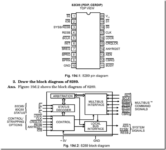
1. Draw the pin connection diagram of 8289.

Ans. The following is the connection diagram of 8289.

10-25-2014 8-38-10 PM

3. Explain how 8289 bus arbiter operates in a multi-master system.

Ans. In MAX mode 8086 processor is interfaced with 8289 bus arbiter, along with bus controller IC 8288 in a multi-master system bus configuration. When the processor does not use the system buses, bus arbiter forces the bus driver output in the high impedance state. The bus arbiter allows the bus controller, the data transreceivers and the address latches to access the system bus.

On a multi-master system bus, the bus arbiter is responsible for avoiding the bus contention between bus masters.

4. How the arbitration between bus masters works?

Ans. The bus is transferred to a higher priority master when the lower priority master completes its task. Lower priority masters get the bus when a higher priority one does not seek to access the bus, although with the help of ANYRQST input, the bus arbiter will allow to surrender the bus to a lower priority master from a higher one. The bus arbiter maintains the bus and is forced off the bus only under HALT instruction.

5. Discuss LOCK and CRQLCK signals.

Ans. Both are active low input signals, the second one standing for Common Request Lock.

A processor generated active low signal on the LOCK output pin is connected to

LOCK input pin of 8289, and prevents the arbiter from surrendering the multi-master system bus to any other bus arbiter, regardless of its priority.

CRQLOCK: An active low on this input pin prevents the arbiter from surrendering the multi-master system bus to any other bus arbiter IC after being requested through CBRQ input pin.

6. Discuss AEN and INIT pins of 8289.

Ans. Both are active low signals, with the former being an output signal and the latter an input signal.

A high on AEN signal puts the output drivers of 8288 bus controller, address latches and the 8284 clock generator into high impedance state.

An active signal (= 0) on INIT input resets all bus arbiters on the multi-master system bus. After initialisation is over, no arbiter can use the said bus.

7. Discuss RESB and SYSB/ RESB pins of 8289.

Ans. Both are input pins for 8289 bus arbiter. RESB and SYSB stand for Resident Bus and System Bus respectively. When RESB is high, the multi-master system bus is requested

or surrendered which is a function of SYSB/ RESB input. When RESB is put to low, SYSB/ RESB input is ignored.

Again, the arbiter requests the multi-master system bus in the System/Resident Mode

when SYSB/ RESB is high and allows the bus to be surrendered when this pin is low.

8. Explain BREQ and BPRO pins.

Ans. Both are active low output pins. The first one stands for Bus Request while the second one stands for Bus Priority Out. BREQ is used in the parallel priority resolving scheme which a particular arbiter activates to request the use of muti-master system bus. BPRO is used in the serial priority resolving scheme and it is daisy-chained to BPRN of the just next lower priority arbiter.

9. Explain BPRN pin.

Ans. It is an active low input and stands for Bus Priority In. When a low is returned to the arbiter, it instructs the same that it may acquire the multi-master system bus on the falling edge of BCLK . The active condition of BPRN indicates that it is the highest priority arbiter presently on the bus. If an arbiter loses its BPRN active signal, it means

that it has lost its bus priority to a higher priority arbiter.

10. Explain BUSY pin.

Ans. It is an active low input-output pin. With the availability of multi-master system bus, the highest priority arbiter seizes the bus, as determined by the status of BPRN input. This thus keeps the other arbiters off the bus. When the particular arbiter has completed its job, it releases the BUSY signal, thereby allowing the next highest arbiter to seize the bus.

11. Explain ANYRQST and CBRQ pins.

Ans. ANYRQST stands for Any Request—it is an active high input pin. CBRQ is, on the other hand, an input/output active low pin and stands for Common Bus Request.

An active signal on ANYRQST would enable the multi-master system bus to be

handed over to an arbiter—even if it has lower priority. When acting as an input, an active condition on CBRQ tells the arbiter of the presence of other lower priority arbiters in the multi-master system bus.

The CBRQ pins of the particular arbiters which would surrender to the multi-master system bus are connected together.

The running arbiter would not pull the CBRQ line low—rather it is done by another arbiter seeking the services which pulls the CBRQ line low. The presently run arbiter then drops its BREQ signal and surrenders the bus, when proper surrender conditions

exist. If CBRQ and ANYRQST are put into active conditions, the multi-master system bus would be surrendered after each transfer cycle.

12. Mention the methods of resolving priority amongst bus masters.

Ans. On a multi-master system bus, there may be several bus masters. The particular bus master which is going to gain control of multi-master system bus is determined by employing bus arbiters. Several techniques are there to resolve this priority amongst bus masters. They are:

z Parallel Priority Resolving Technique.

z Serial Priority Resolving Technique.

z Rotating Priority Resolving Technique.

13. Discuss the Parallel Priority Resolving Technique.

Ans. The technique of resolving priority in this scheme is shown in Fig. 19d.3. Four arbiters have been shown each of whose BREQ (Bus Request) output line is entered into apriority encoder and then to a decoder. The BPRN (Bus Priority In) output lines of the encoder are returned—one each to each of the arbiters.

10-25-2014 8-38-50 PM

But corresponding to the highest priority active BREQ , an active BPRN is obtained, which activates the respective bus arbiter, neglecting the lower priority BREQ’s .

Thus the bus master corresponding to this bus arbiter will identify itself with the multi- system bus master or would wait until the present bus transaction is complete.

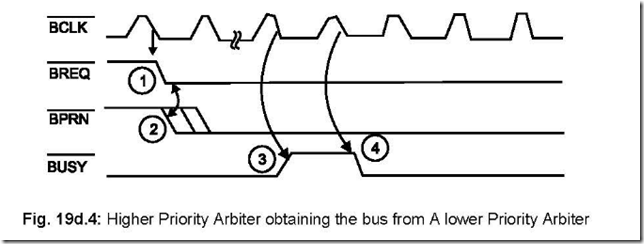
Fig. 19d.4 shows the waveform timing diagrams of BREQ, BPRN and BUSY signals, which are synchronised with BLCK . The explanation of the waveform timing diagram is as follows. When the bus cycles are running, the BREQ line goes low [ 1 ]. There can be more than one BREQ line going low during this time. But the 74HC138 3 to 8 decoder would output a low on that particular BPRN [ 2 ] which corresponds to the

10-25-2014 8-39-11 PM

clip_image021[6]clip_image021[7]thereby pulling it off from the multi-master system bus. In the next BLCK cycle, the arbiter which just had the right to use the system bus, pulls its own BUSY line low,

thereby making it active and at the same time forcing other arbiters off the bus.

14. Discuss the Serial Priority Resolving Technique.

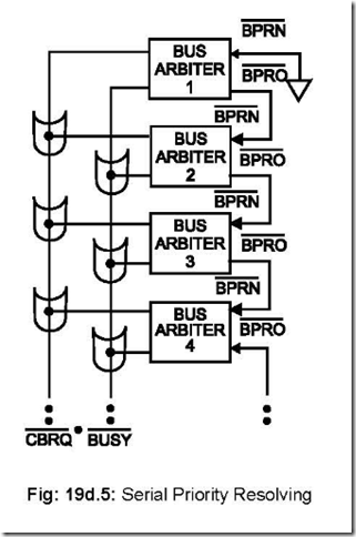
Ans. Figure 19d.5 shows the technique employed in this scheme. This scheme does away with the hardware combination of encoder-decoder logic as employed in Parallel Priority

clip_image056Scheme. Instead, the higher priority bus arbiter’s BPRO (Bus Priority Out) is fed to the BPRN (Bus Priority In) of the just next lower priority one.

10-25-2014 8-39-25 PM

15. Discuss Rotating Priority Resolving Technique.

Ans. In this scheme, the priority, to get the right to use the multi-master system bus, is dynamically reassigned. The circuitry is so designed that each of the requesting arbiters gets an equal chance to use the multi-master system bus.

16. Compare the three types of Priority Resolving Techniques.

Ans. In the serial priority scheme, the number of arbiters that may be daisy-chained together

clip_image038[3]is a function of BLCK , as well as the propagation delay that exists from one arbiter to the next one. With a 10 MHz frequency of operation, a maximum of 3 arbiters can be so connected.

The rotating priority resolving technique employs a considerable amount of external

logic for its implementation. The parallel priority resolving technique is a good

compromise compared to the other two in the sense that it employs a moderate amount

of hardware to implement it while at the same time accommodating a good number of

arbiters.

17. Discuss the modes of operations of 8289.

Ans. 8289 bus arbiter provides support to two types of processors : 8089 I/O Processor and 8086/8088. Thus 8289 supports two modes of operations—(a) IOB (I/O Peripheral Bus) mode —which permits the processor access to both I/O peripheral bus and a multi-master system bus. When 8289 needs to communicate with system memory, this is effected with the help of system memory bus. (b) RESB (Resident Bus) mode—which permits the processor to access to resident bus and a multi-master system bus.

All devices residing on IOB are treated as I/O devices (including memory) and are all addressed by I/O commands, the memory commands being handled by multimaster system bus. A Resident Bus can also issue both memory and I/O commands—but distinct from the multi-master system bus. The Resident Bus has only one master.

clip_image059clip_image060When IOB = 0 , 8289 is in IOB mode and when RESB = 1, 8289 is in RESB mode. When IOB =0 and RESB = 1, then 8089 interfaces with 8086 to a multi-master system

clip_image060[1]bus, a Resident Bus and an I/O Bus. Again, for IOB = 1 and RESB = 0, 8089 interfaces with 8086 to a multi-master system bus only.


8089 I/O Processor

8089 I/O Processor

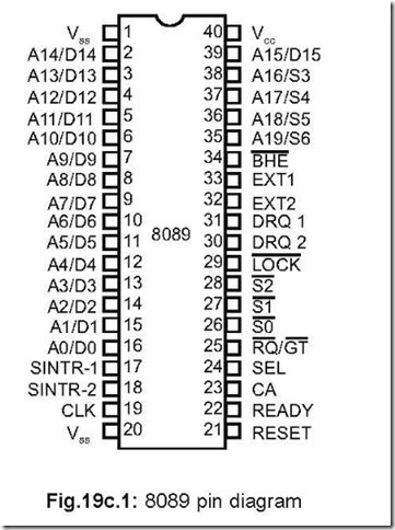
1. Draw the pin connection diagram of 8089.

Ans. The pin connection diagram of 8089 is shown in Fig. 19c.1.10-25-2014 8-35-58 PM

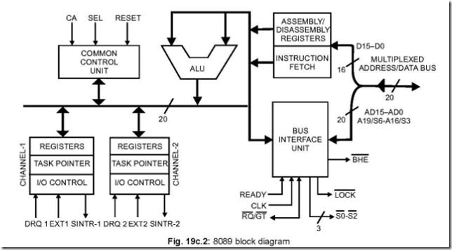
2. Draw the functional block diagram of 8089.

Ans. The functional block diagram of 8089 is shown in Fig. 19c.2.

10-25-2014 8-36-24 PM

3. Write down the characteristic features of 8089. Ans. The characteristic features of 8089 are as follows:

z Very high speed DMA capability—I/O to memory, memory to I/O, memory to

memory and I/O to I/O.

z 1 MB address capability.

z iAPX 86, 88 compatible.

z Supports local mode and remote mode I/O processing.

z Allows mixed interface of 8-and 16-bit peripherals, to 8-and 16-bit processor buses.

z Multibus compatible system interface.

z Memory based communications with CPU.

z Flexible, intelligent DMA functions, including translation, search, word assembly/

disassembly.

z Supports two I/O channels.

4. Indicate the data transfer rate of 8089 IOP.

Ans. On each of the two channels of 8089, data can be transferred at a maximum rate of 1.25 MB/second for 5MHz clock frequency.

5. Mention a few application areas of 8089. Ans. A few of the application areas of 8089 are:

z File and buffer management in hard disk/floppy disk control.

z Provides for soft error recovery routines and scan control.

z CRT control such as cursor control and auto scrolling made simple with 8089.

z Keyboard control, communication control, etc.

6. Compare 8089 IOP with 8255 PPI and 8251 USART.

Ans. 8089 IOP is a front-end processor for the 8086/88 and 80186/88. In a way, 8089 is a microprocessor designed specifically for I/O operations. 8089 is capable of concurrent

operation with the host CPU when 8089 executes a program task from its own private memory.

8255 PPI and 8251 USART are peripheral controller chips designed to simplify I/O hardware design by incorporating all the logic for parallel (in case of 8255) or serial (in case of 8251) ports in one single package. These two chips need to be initialized for them to be used. But data transfer is controlled by CPU.

8089 IOP does not have any built-in I/O ports, not it is a replacement for 8255 or 8251. For I/O operations, 8089 executes the I/O related softwares, previously run by CPU (when no 8089 was used).

Thus in situations where I/O related operations are in a majority, 8089 does all these jobs independent of CPU. Once done, the host CPU communicates with 8089 for high speed data transfer either way.

7. Does 8089 generate any control signals.

Ans. No, 8089 does not output control bus signals: IOW, IOR, MEMR, MEMW, DT/ R, ALE and DEN. These signals are encoded into S0 − S2 signals, which are output pins for 8089 and are connected to the corresponding pins of 8288 bus controller and 8289

bus arbiter to generate memory and I/O control signals. The bus controller then outputs

all the above stated control bus signals. The S0 − S2 signals are encoded as follows

10-25-2014 8-36-42 PM

These signals change during T4 if a new cycle is to be entered. The return to passive state in T3 or TW indicates the end of a cycle. These pins float after a system reset— when the bus is not required.

8. Explain the utility of LOCK signal.

Ans. It is an output signal and is set via the channel control register and during the TSL instruction. This pin floats after a system reset—when the bus is not required.

The LOCK signal is meant for the 8289 bus arbiter and when active, this output pin prevents other processors from accessing the system buses. This is done to ensure that the system memory is not allowed to change until the locked instructions are executed.

9. Explain DRQ1-2 and EXT1-2 pins.

Ans. DRQ and EXT stand for Data Request and External Terminate, both being input pins— DRQ1 and EXT1 for channel 1 and DRQ2 and EXT2 for channel 2.

DRQ is used to initiate DMA transfer while EXT for termination of the same. A high on DRQ1 tells 8089 that a peripheral is ready to receive/transfer data via channel 1. DRQ must be held active (= 1) until the appropriate fetch/stroke is initiated.

A high on EXT causes termination of current DMA operation if the channel is so programmed by the channel control register. This signal must be held active (= 1) until termination is complete.

10. Explain the common control unit (CCU) block.

Ans. 8089 IOP has two channels. The activities of these two channels are controlled by CCU. CCU determines which channel—1 or 2 will execute the next cycle. In a particular case where both the channels have equal priority, an interleave procedure is adopted in which each alternate cycle is assigned to channels 1 and 2.

11. Explain the purpose of assembly/disassembly registers.

Ans. This permits 8089 to deal with 8-or 16-bit data width devices or a mix of both. In a particular case of an 8–bit width I/O device inputting data to a 16-bit memory interface, 8089 capture two bytes from the device and then write it into the assigned memory locations—all with the help of assembly/disassembly register.

12. Explain SINTR pin.

Ans. SINTR stands for signal interrupt. It is an output pin from 8089 and there are two such output pin SINTR1 and SINTR2—for channel 1 and 2 respectively.

Like 8087, 8086 does not communicate with 8089 directly. Normally, this takes place via a series of commonly accessible message blocks in system memory.

SINTR pin is another method of such communication. This output pin of 8087 can

be connected directly to the host CPU (8086) or through an 8259 interrupt controller. A high on this pin alerts the CPU that either the task program has been completed or else an error condition has occurred.

13. Elaborate on the communication between CPU and IOP with the help of communication data structure hierarchy.

Ans. Communication between the CPU and IOP takes place through messages in shared memory and consists of five linked memory message blocks (ABCDE or ABCD′E′ ) with ABC representing the initialisation process. The process of initialisation begins with 8089 IOP receiving a reset at its RESET input. The following occurs in sequence:

z On the falling edge of CA, the SEL input is sensed. SEL = 0/1 represent Master (Remote)/Slave (Local) configuration. (To note: during any other CA, the SEL line indicates selection of CH1/CH2 depending on SEL = 0/1 respectively).

z 5 bytes of information from system memory starting from FFFF6 H is read into 8089.

The first byte determines the width of the system bus. The subsequent bytes are then read to get the system configuration pointer (SCP) which gives the locations of the system configuration block (SCB).

clip_image029clip_image030z The first byte existing at the base of SCB is read off, which determines the width of the 8089’s Private Bus and the operating mode of RQ / GT is defined. The base (or starting) address of control block (CB) is then read.

z The BUSY flag in CB is removed, signalling the end of the initialisation process.

It should be noted that the address of SCP—the system configuration pointer resides

in ROM and is the only one to have fixed address in the hierarchy. Since SCB resides

in RAM, hence it can be changed to accommodate additional IOPs, to be inducted into

the system.

10-25-2014 8-37-10 PM

All except the task block must be located in memory accessible to the 8089 and the host processor.

Once initialisation is over, any subsequent hardware CA input to IOP accesses the control block (CB) bytes for a particular channel—the channel (1 or 2) which gets selected depends on the SEL status. First the CCW (Channel Control Word) is read. Next the base address for the parameter block (PB) is read. This is also called data memory. Except the first two words, this PB block is user defined and is used to pass appropriate parameters to IOP for task block (TB), also called program memory. The task block can be terminated/restarted by the CPU.

This hierarchical data structure between the CPU and IOP gives modularity to system design and also future compatibility to future end users.

14. Show the channel register set model and discuss. Ans. The channel register set for 8089 IOP is shown in Fig.19c.4.

10-25-2014 8-37-36 PM

Registers GA, GB and GC and TP may address 1 MB of memory space (with tag bit = 0) or 64 KB of I/O space (with tag bit = 1). These four registers as also PP are called pointer registers.

The rest four registers—IX, BC, MC and CC are all 16 bits wide. Several DMA options can be programmed with the help of register CC.

15. Mention the addressing modes of 8089 IOP.

Ans. 8089 IOP has six different addressing modes. These are:

z Register addressing

z Immediate addressing

z Offset addressing

z Based addressing

z Indexed addressing and

z Indexed with auto increment addressing.


8087 Numeric Data Processor

8087 Numeric Data Processor

1. Draw the pin connection diagram of 8087. Ans. The pin diagram of 8087 is shown in Fig. 19b.1.

10-25-2014 8-33-45 PM

2. What are the characteristics of 8087 NDP?

Ans. The following are the characteristic features of 8087 NDP:

z It can add arithmetic, trigonometric, exponential and logarithmic instructions to the

8086 instruction set for all data types.

z 8087 can handle seven data types. These are : 16, 32, 64-bit integers, 32, 64, 80-bit

floating point and 18–digit BCD operands.

z It has three clock speeds: 5 MHz (8087), 8 MHz (8087–2) and 10 MHz (8087–1)

z It can add 8 × 80-bit individually addressable register stack to the 8086 architecture.

z Multibus system compatiable interface.

z Seven numbers built-in exception handling functions.

z Compatible with IEEE floating point standard 754.

z It adds 68 mnemonics to the 8086 instruction set.

z Fabricated with HMOS III technology and packaged in a 40-pin cerdip package.

3. Draw the architecture of 8087.

Ans. The architecture of 8087 is shown below in Fig. 19b.2.

10-25-2014 8-34-22 PM

4. How does 8086 view 8087 NDP?

Ans. At the hardware level, 8086 treats 8087 as an extension to its own CPU capability— providing for registers, data types, control and instruction capabilities.

At the software level, both 8086 and 8087 are viewed as a single unified processor.

5. Discuss A16/S3 to A19/S6 signals.

Ans. When 8086 CPU is in control of buses, these four lines act as input lines, which 8087 monitors.

When 8087 controls the buses, these are the four most significant address lines (A19 to A16) for memory operations during T1. Also, during T2, T3, Tw and T4, status information is available on these four lines. During these states, S6, S4 and S3 are high while S5 is always low.

6. clip_image006clip_image007clip_image006[1]Discuss the S2, S1 and S0 signals.

Ans. These three signals act as both input or output pins.

When the CPU is active, i.e., CPU is in control of buses, these three signals act as

input pins to 8087. 8087 monitors these signals coming from 8086.

When 8087 is driving, these three status lines act as output pins and are encoded as

follows:

10-25-2014 8-34-37 PM

The status lines are driven active during T4, remains valid during T1 and T2 and returns to passive state (111) in T3 or Tw, when READY is high. The status on these lines are monitored by 8288 to generate all memory access control signals.

7. What language 8087 supports?

Ans. 8087 supports the high level languages of 8086 which are: ASM-86, PL/M-86, FORTRAN-86 and PASCAL-86.

8. How 8-bit and 16-bit hosts are taken care of by 8087?

Ans. For 8-bit and 16-bit hosts, all memory operations are performed as byte or word operations respectively.

clip_image011clip_image0128087 determines the bus width during a system reset by monitoring pin 34 (BHE / S7) of 8087. For 16-bit hosts a word access from memory locations FFFF0 H (a dedicated location) is performed and pin 34 ( BHE ) will be low while, for a 8-bit host, a byte access

clip_image013from the same memory location FFFF0 H is performed and pin 34 ( SS0 ) will be high.

9. What is the operating frequency of 8087?

Ans. 8087 operates at frequencies of 5 MHz, 8 MHz and 10 MHz.

10. What is the utility of having NDP 8087 along with 8086?

Ans. 8086 is a general purpose microprocessor suitable mostly for data processing applications.

But in cases where scientific and other calculation-intensive applications are involved,

8086 fails with its integer arithmetic and four basic math function capabilities.

8087 can process fractional number system and transcendental math functions with

its special coprocessor instructions in parallel with the host CPU—thus relieving 8086

with these tasks. In Intel number scheme, 8086/8087 system is known as an iAPX86/20

two-chip CPU.

11. What are the two units in NDP and what do they do?

Ans. There are two units in 8087—a Control Unit (CU) and a Numeric Execution Unit (NEU).

These two units can operate independently i.e., asynchronously—like the BIU and

EU of 8086.

The CU receives, decodes instructions, reads and writes memory operands and

executes all other control instructions. NEU does the job of arithmetic processing. The

control unit establishes the communication between the CPU and memory and

coordinates the internal processor activities.

12. How 8086 communicates with NDP 8087?

clip_image014clip_image015clip_image016Ans. The opcodes for 8087 are written into memory along with those for 8086. As 8086 (host) fetches instructions from memory, 8087 also does the same. These prefetched instructions

are put into the queue of both 8086 and 8087, while S0 , S1

information on bus status.

and S2

provide the

When an ESC instruction is encountered by the host (8086), it calculates the effective

address (EA) and performs a ‘dummy’ read cycle. The data read is not stored. However,

a read or write cycle is performed by 8087 from this EA. 8087 does not have any facility

to generate EA on its own. If the coprocessor instruction does not need any memory

operand, then it is directly executed by 8087.

Several data formats as used by 8087 require multiple word memory operands. In such

cases, 8087 need to have the buses under its own control. This is achieved via RQ/GT

line. The sequence is as follows:

z 8087 sends out a low going pulse on its RQ/GT pin (connected to the RQ/GT pin of

8086) of one clock pulse duration.

z 8087 waits for the grant pulse from the host (8086).

z When it is received by 8087, it increments the address and outputs the incremented

address on the address bus.

z 8087 continues memory-read or memory-write signals until all the instructions meant

for 8087 are complete.

z At this point, another low going pulse is sent out by 8087 (to 8086) on its RQ/GT line,

to let 8086 know that it can have the buses back again.

When the NEU (numeric execution unit) begins executing arithmetic, logical,

transcendental and data transfer instructions, it (8087) pulls up BUSY signal. This output

clip_image017signal of 8087 is connected to the TEST input of 8086. This forces 8086 to wait until the

clip_image018TEST input of 8086 goes low (i.e., BUSY output of 8087 becomes low).

The microcode control unit of 8087 generates the control signals for execution of instructions while the ‘programmable shifter’ shifts the operands, during the execution of instructions like FMUL and EDIV. The data bus interfaces the internal data bus of 8087 with the data bus of the host (8086).

13. What INT output signal does?

Ans. This interrupt output is utilised by 8087 to indicate that an unmasked exception has been received during excitation by 8087. This is normally handled by 8259A.

14. clip_image019Discuss the BHE/S7 signal of 8087.

clip_image020Ans. During T1 cycle, BHE / S7 output pin used to enable data on the higher byte of the 8086 data bus. During T2, T3, Tw and T4, this pin becomes the status line S7.

15. What kind of errors/exception conditions 8087 can check?

Ans. During execution of instructions, 8087 can check the following kind of errors/exception conditions:

z Invalid operation: This includes the attempt to calculate the square root of a negative number or say to take out an operand from an empty register. Also included in this category are stack overflow, stack underflow, indeterminate form or the use of a non-number as an operand.

z Overflow: Exponent of the result is too large for the destination real format.

z Zero divide: Arises when divisor is zero while the dividend is a non-infinite,

non-zero number.

z Denormalised: It arises when an attempt is made to operate on an operand that

is yet to be normalised.

z Under flow: Exponent of the result is too small to be represented.

z Precision: In case the operand is not made to represent in the destination format,

causing 8087 to round the result.

16. What does 8087 do in case an exception occurs?

Ans. 8087 sets the appropriate flag bit in the status word in case of occurrence of any one of the exception conditions. The exception mask in the control register is then checked and if the mask bit is set i.e., masked, then a built-in fix-up procedure is followed.

If the exception is unmasked (i.e., mask bit = 0), then user-written exception handlers take care of such situations. This is done by using the INT pin which is normally connected to one of the interrupt input pins of 8259A PIC.

17. Describe the register set of 8087.

Ans. The register set of 8087 comprises the following:

z Eight data registers—each 80-bits wide

z A tag field R1–R8.

z Five control/status registers.

The register set of 8087 is shown in Fig. 19b.3.

10-25-2014 8-35-00 PM

The eight data registers, residing in NEU, can be used as a stack or a set of general registers. These registers are divided into three fields—sign (1-bit), exponent (15-bits) and significand (64-bits). Corresponding to each of these eight registers, there is a two bit TAG field to indicate the status of contents.

The control and status registers are shown in Fig. 19b.4. The top bits in the status register indicate the register currently at the top of the register stack. Bits 0–5 indicate the ‘exception’ status, while the condition code bits C2 – C0 are set by various 8087 operations similar to the flags within the CPU.

10-25-2014 8-35-21 PM

Bits 0 – 5 of the control word register allow any of the exception cases to be masked. Bit 6 is a ‘don’t care’ bit while bit 7 must be reset (low) for the interrupts to be accepted. The upper bits of the control register defines type of infinity, rounding and precision to be used when 8087 performs the calculations.

The control register defines the type of infinity, rounding and precision to be used

when NDP performs and executes the instructions. For the interrupts to be accepted,

bit 7 must be reset while bits 0–5 allow any of the exception cased to be masked.

Both the Data & Instruction pointer registers are 20-bits wide. Whenever the NEU executes an instruction, CU saves the opcode and memory address corresponding to this instructions and also its operand in these registers. For this, a control instruction is needed for their contents to be stored in memory and is utilised for program debugging.

Initially, Data registers of 8087 are considered to be empty, unlike the CPU registers. The data written into these registers can be valid (i.e., the register holds a valid data in temporary real format), zero or special (indefinite due to error). Each data register has a tag field associated with the corresponding register. Each tag field is two bit wide and contains one of the four states that each of the data registers can hold. The eight numbers of 2-bit tag field again are grouped into a single tag word—it is thus 16-bit wide. It optimises the NDP’s performance under certain conditions and normally needed by the programmer.


8288 Bus Controller

8288 Bus Controller

1. Draw the pin diagram of 8288.

8288 Bus Controller 8-25-53 PM

2. Draw the functional block diagram of 8288.

Ans. The functional block diagram of 8288 is shown in Fig. 19a.2.

8288 Bus Controller 8-26-26 PM

3. Is 8288 always used with 8086?

Ans. No, the bus controller IC 8288 is used with 8086 when the latter is used in MAX mode.

4. What are the inputs to 8288?

Ans. There are two sets of inputs—the first set is the status inputs S0 , S1 and S2 . The second set is the control inputs having the following signals: CLK, AEN, CEN and IOB.

5. What are the output signals from 8288?

Ans. There are two sets of output signals—Multibus command signals and the second set includes the bus control signals—Address Latch, Data Transreceiver and Interrupt Control Signals.

The multibus command Signals are the Conventional MEMR, MEMW, IOR and IOW signals which have been renamed as MRDC, MWTC, IORC, IOWC, where the suffix ‘C’ stands for command. INTA signal is also included in this.

Two more signals— AMWC and AIOWC are the advanced memory and I/O write

commands. These two output signals are enabled one clock cycle earlier than normal write commands. Some memory and I/O devices require this wider pulse width.

The bus control signals are DT/ R , DEN, ALE and MCE/ PDEN . The first three are identical to 8086 output signals when operated in the MIN mode—with the only difference here is that the DEN output signal of 8288 is an active high signal.

MCE/ PDEN (Master Cascade Control/Peripheral Data Enable) is an output signal having two functions—I/O bus control or system bus control. When this signal status is low, its function is identical to DEN signal and it operates in I/O mode. When high, this signal ensures the sharing of the system buses by other processors connected to the system.

In the system bus control mode, the signals AEN (address enable) and IOB both have to be low. This then permits more than one 8288 and 8086 to be interfaced to the same set of system buses. In this case, the bus arbiter IC 8289 selects the active processor by

enabling only one 8288, via the AEN input. In this system bus mode MCE/ PDEN signal becomes MCE-Master Cascade Control and is used during an interrupt sequence to read the address from a master priority interrupt controller (PIC).

The operating modes of 8288 are determined by CEN (command enable), IOB,

clip_image040(I/O bus) and AEN signals and shown in Table 19a.1.

8288 Bus Controller 8-26-51 PM

6. Discuss the status pins S2 , S1 and S0 .

Ans. These are three input pins for 8288 and come from the corresponding pins of 8086 (its output pins). The command-decode definitions for various combinations of the three signals are shown in Table 19a.2.

8288 Bus Controller 8-27-09 PM

7. Discuss the three pins (a) IOB (b) CEN and (c) AEN of 8288.

Ans. (a) IOB stands for input/output bus mode and is an input signal for 8288. When IOB = high, 8288 functions in the I/O bus mode and when IOB = low, 8288 functions in the system bus mode.

(b) CEN stands for command enable and is an input signal for 8288. When

CEN = low, all command outputs of 8288 and the DEN and the PDEN control outputs

are forced into active state and not tri-stated. This feature is utilised for memory

partitioning implementation. This also eliminates address conflicts between system

bus devices and resident bus devices. Again, when CEN = high, these outputs are in

the enabled state.

(c) clip_image040[1]AEN stands for address enable and is an input signal for 8288. This signal enables command outputs of 8288 a minimum of 110 ns (and a maximum of 250 ns) after it

clip_image039[3]clip_image052becomes low (i.e., active). If AEN = 1, then command output drivers are put to tri-state. In the I/O bus mode (IOB = 1) AEN signal does not affect the command lines.


8086 Interrupts

8086 Interrupts

1. How many interrupts can be implemented using 8086 µP?

Ans. A total of 256 interrupts can be implemented using 8086 µP.

2. Mention and tabulate the different types of interrupts that 8086 can implement. Ans. 8086 µP can implement seven different types of interrupts.

z NMI and INTR are external interrupts implemented via Hardware.

z INT n, INTO and INT3 (breakpoint instruction) are software interrupts implemented

through Program.

z The ‘divide-by-0’ and ‘Single-step’ are interrupts initiated by CPU.

Table 18.1 shows the seven interrupt types implemented by 8086.

8086 Interrupts8-07-08 PM

3. Distinguish between the two hardware interrupts of 8086.

Ans. The distinction between the two hardware interrupts of 8086 are as follows, shown in Table 18.2.

Table18.2: Comparison of NMI and INTR interrupts

NMI

INTR

1. Non-maskable type.

2. Higher priority.

3. Edge triggered interrupt initiated on Low to High transition.

4. Must remain high for more than 2 CLK cycles.

5. The rising edge of NMI input is latched on-chip and is serviced at the end of current instruction.

6. No acknowledgement.

1. Maskable type.

2. Lower priority.

3. Level triggered interrupt.

4. Sampled during last CLK cycle of each instruction.

5. No latching. Must stay high until acknowledged by CPU.

6. Acknowledged by INTA output signal.

4. How many bytes are needed to store the starting addresses of ISS for 8086 µP? Ans. 8086 µP can implement 256 different interrupts. To store the starting address of a single ISS (Interrupt Service Subroutine), four bytes of memory space are required—two bytes

to store the value of CS and two bytes to store the IP value. Thus to store the starting address of 256 ISS, in all 256 × 4 = 1024 bytes = 1 KB will be required.

5. Indicate the number of memory spaces needed in stack when an interrupt occurs.

Ans. When an interrupt occurs, before moving over to starting address of the corresponding ISS, the following are pushed into the stack: the contents of the flag register, CS and IP. Since each one of the three are 2 bytes, hence a total of 6 bytes of memory space is needed in the stack to accommodate the flag register, CS and IP contents.

6. What are meant by interrupt pointer and interrupt pointer table?

Ans. The starting address of an ISS in the 1 KB memory space is known as the interrupt pointer or interrupt vector corresponding to that interrupt.

The 1 KB memory space needed to store the starting addresses of all the 256 ISS is called the interrupt pointer table.

7. Write down the steps, sequentially carried out by the systems when an interrupt occurs.

Ans. When an interrupt occurs (hardware or software), the following things happen:

z The contents of flags register, CS and IP are pushed on to the stack.

z TF and IF are cleared which disable single step and INTR interrupts respectively.

z Program jumps to the starting address of ISS.

z At the end of ISS, when IRET is executed in the last line, the contents of flag register,

CS and IP are popped out of the stack and placed in the respective registers.

z When the flags are restored, IF and TF get back their previous values.

8. Draw and discuss the interrupt pointer table for 8086 µP. Ans. The interrupt pointer table for 8086 is shown in Fig. 18.1.

8086 Interrupts8-08-07 PM

The 256 interrupt pointers are stored in memory locations starting from 00000 H to 003FF H (1 KB memory space). The number assigned to an interrupt pointer is called

the Type of the corresponding interrupt. As for example, Type 0 interrupt, Type 1 interrupt … Type 255 interrupt. Type 0 interrupt has a memory address 00000 H, Type 1 has a memory address 00004 H, while Type 255 has a memory address 003FF H. The first five pointers (Type 0 to Type 4) are dedicated pointers used for divide by zero, single step, NMI, break point and overflow interrupts respectively. The next 27 pointers (Type 5 to Type 31) are reserved pointers—reserved for some special interrupts. The remaining 224 interrupts—from Type 32 to Type 255 are available to the programmer for handling hardware and software interrupts.

9. Discuss the priority of interrupts of 8086.

Ans. 8086 tests for the occurence of interrupts in the following hierarchical sequence:

z Internal interrupts (divide-by-0, single step, break point and overflow)

z Non-maskable interrupt—via NMI

z Software interrupts—via INTn

z External hardware interrupt—via INTR

Hence, internal interrupts belong to the highest priority group and internal hardware

interrupts are the lowest priority group. Again, different interrupts are given different

priorities by assigning a type number corresponding to each priority—starting from

Type 0 (highest priority interrupt) to Type 255 (lowest priority interrupt). Thus, Type 40

interrupt is having more priority than Type 41 interrupt. If we presume that at any

instant a Type 40 interrupt is in progress, then it can be interrupted by any software

interrupt, the non-maskable interrupt, all internal interrupts or any external interrupt

with a Type number less than 40.

10. Outline the events that take place when 8086 processes an interrupt.

Ans. Fig. 18.2 shows the manner in which 8086 processes an interrupt while the following are the events that take place sequentially when the processor receives an interrupt (from an external device via INT 32 through INT 255:

z Receiving an interrupt request (from an external device)

z Generation of interrupt acknowledge bus cycles.

z Servicing the Interrupt Service Subroutine (corresponding to the external device

which has interrupted the CPU.)

Again the difference between simultaneous interrupt and interrupt within an ISS is

to be understood. Occurrence of more than one interrupt within the same instruction is

called simultaneous interrupt while if an interrupt occurs while the ISS is in progress,

it is an interrupt occurring within an ISS.

Internal interrupts (except single step) have priority over simultaneous external

requests. For example, let the current instruction causes a divide-by-zero interrupt when

an INTR (a hardware interrupt) occurs, the former will be serviced. Again, if

simultaneous interrupts occur on INTR and NMI, then NMI will be serviced first.

For simultaneous interrupts occurring, the priority structure of Fig.18.2 will be

honoured, with the highest priority interrupt being serviced first.

Although it has been commented that software interrupts get priority over external

hardware interrupts, even then if an interrupt on NMI occurs as soon as the interrupt’s

ISS begins, it (i.e., NMI) will be recognised and hence serviced.

8086 Interrupts8-08-28 PM

11. List the different interrupt instructions associated with 8086 µP.

Ans. Table 18.3 lists the different interrupts of 8086 µP along with a brief description of their

functions.8086 Interrupts8-08-51 PM12. Show the internal interrupts and their priorities.

Ans. The internal interrupts are: Divide-by-0, single step, break point and overflow corresponding to Type 0, Type 1, Type 3 and Type 4 interrupts respectively.

Since a type with lesser number has higher priority than a type with more number, thus the mentioned internal interrupts can be arranged in a decreasing priority mode, with highest priority mentioned first: Divide-by-0, single step, break point, overflow.

13. What are the characteristics associated with internal interrupts? Ans. The following are the characteristics associated with internal interrupts:

z The interrupt type code is either contained in the instruction itself or is predefined.

clip_image012z No INTA bus cycles are generated, as in the case of INTR interrupt input.

z Apart from single step interrupt, no other internal interrupt can be disabled.

z Internal interrupts, except single step have higher priority than external interrupts.

14. Discuss the two interrupts HLT and WAIT.

Ans. On execution of HLT (halt) instruction by 8086, CPU suspends its instruction execution and enters into an idle state. It waits for either an external hardware interrupt or a reset input (interrupt). When any one of these occurs, CPU starts executing again.

When the WAIT instruction is executed by 8086, it internally checks the logic level

clip_image013clip_image014clip_image015existing at its TEST input. If TEST is at logic 1 state, then CPU goes into an idle state. When TEST input assumes a zero state, execution resumes from the next sequential

clip_image014[1]instruction in the program. TEST input is normally connected to the BUSY output signal of 8087 NDP.

15. Mention the addresses at which CS40 and IP40 corresponding to vector 40 would be stored in memory.

Ans. INT 40, for its storage, requires four memory locations—two for IP40 and two for CS40.

The addresses are calculated as follows:

1

4 × 40 = 160 10= 1010 0000=  A0 H.

2

Thus, IP40 is stored starting at 000A0 H and CS40 is stored starting at 000A2 H.

16. Explain in detail the external hardware interrupt sequence.

Ans. The external device can request for service via INT 32 through INT 255 by pulling the corresponding INT n (n = 32 to 255) high. The interrupt request gives rise to generation of interrupt acknowledge bus cycles and then moving into ISS corresponding to the device which has interrupted the system. The presently requested interrupt is recognised provided no higher priority interrupt is pending and IF is already set via software.

Once the interrupt is recognised (since for any INTR to be recognised, the corresponding INT must stay high till the last clock cycle of the presently executed instruction). 8086 initiates interrupt acknowledge bus cycles, shown in Fig. 18.3.

During T1 of the first interrupt bus cycle, ALE is put to low state and remains so till the end of the cycle. During the whole of this cycle, address/data bus is driven into

clip_image016Z-state. During T2 and T3 of this first interrupt bus cycle, INTA is put to low state— indicating that the request for service has been granted so that the requesting device can withdraw its high logic which is connected to INTR pin 8086.

LOCK signal is of importance only in maximum mode. This signal goes low during T2 of the first INTA bus cycle and is maintained in zero state until T2 of the second INTA bus cycle.

8086 Interrupts8-09-18 PM

8086 is prevented from accepting a HOLD request. The LOCK output, in conjunction with external logic, is used to lock off other devices from the system bus. This ensures completion of the current interrupt till its completion.

During the second interrupt bus cycle, the external circuit puts in the interrupt code

(3210 = 20 H through 25510 = FF H) on the data bus AD0– AD7 during T3 and T4 and is read by 8086.

Before moving to ISS, CPU saves the contents of the flag register along with the current CS and IP values. Now by reading the number from the data bus, the corresponding CS and IP values are placed in them (for instance, if the external device has interrupted via INT 60, then CS60 and IP60 would be loaded into CS and IP register

respectively). Thus the ISS would be run to its completion because before moving into

ISS, IF and single-stepping have been disabled.

In the last line of ISR, an IRET instruction is there, which on its execution pops the old CS and IP values from the stack and put them in CS and IP registers. This thus ensures that the main program starts at the very memory location that was left off because of ISS.

17. Indicate two applications where NMI interrupt can be applied.

Ans. NMI is a non-maskable hardware interrupt, i.e., it cannot be masked or disabled. Hence, it is used for very important system exigencies like (a) detection of power failure or

(b) detection of memory read error cases.

18. Draw a circuit that will terminate the INTR when interrupt request has been acknowledged.

Ans. Fig. 18.4 makes INTR input of 8086 to go into 1 state once the interrupt request comes from some external agency. The falling edge of the peripheral clocks the flip-flop which

clip_image026makes INTR to become 1. The first INTR pulse then resets Q, making INTR to become

0. This ensures that no second interrupt request is recognised by the system. The reset input sees to it that INTR remains in the 0 state when the system is reset.

8086 Interrupts8-09-40 PM

19. Discuss the following (a) Type 0 interrupt (b) Type 1 interrupt (c) Type 2 interrupt (d) Type 3 interrupt and (e) Type 4 interrupt.

Ans. (a) Type 0 interrupt (or Divide-by-zero interrupt)

If the quotient resulting from a DIV (divide) instruction or an IDIV (integer divide) instruction is too large such that it cannot be accommodated in the destination register, a divide error occurs. Then 8086 perform a Type 0 interrupt. This then passes the control to a service subroutine at addresses corresponding to IP0 and CS0 at 0000 H and 0002 H respectively in the pointer table.

(b) Type 1 interrupt (Single Step interrupt)

The single step interrupt will be enabled only if the trap flag (TF) bit is set (= 1). The TF bit can be set/reset by software.

Single step control is used for debugging in assembly language. In this mode the processor executes one instruction and then stops. The contents of various registers and memory locations can be examined. If the results are found to be ok, then a command can be inserted for execution of the next instruction. Trap flag cannot be set directly. This is done by pushing the flags on the stack, changes are made and then they are popped.

(c) Type 2 interrupt (non-maskable NMI interrupt)

Type 2 interrupt is the non-maskable NMI interrupt and is used for some emergency

situations like power failure. When power fails, an external circuit detects this and

sends an interrupt signal via NMI pin of 8086. The DC supply remains on for atleast 50 ms via capacitor banks so that the program and data remaining in RAM locations can be saved, which were being executed at the time of power failure.

(d) Type 3 interrupt (break point interrupt)

Type 3 interrupt is a break point interrupt. The program runs up to the break point

when the interrupt occurs. This is achieved by inserting INT 3 at the point the break

is desired. The ISS corresponding to Type 3 interrupt saves the register contents in the stack and can also be displayed on CRT and the control is returned to the user. This is used as a software debugging tool, like single stepping method.

(e) Type 4 interrupt (overflow interrupt)

The software instruction INTO (interrupt on overflow) is inserted in a program

immediately after an arithmetic operation is performed. Insertion of INTO implements

a Type 4 interrupt. When the signed result of an arithmetic operation on two signed numbers is too large to be stored in the destination register or else in a memory location, an overflow occurs and the OF (overflow flag) is set. This initiates INT4 instruction and the program control moves over to the starting address of the ISS, which corresponds to IP4 and CS4. These two are stored at address locations 0010 H and 0012 H respectively.

20. In what way the INTO instruction is different from others?

Ans. The INTO instruction is different in that no type number is needed to be mentioned.

To explain the difference, for executing any INT instruction, type no. is needed, like

INT 10, INT 23, etc.

To explain further,

Opcode

Operand

Object Code

Mnemonic

INT

INTO

Type

none

CD 23

CE

INT 23 H (assuming Type 23 H is employed)

INT

21. Draw the schemes of (a) Min and (b) Max mode 8086 system external hardware interrupt interface and explain.

Ans. (a) The scheme of interconnections of Min-mode 8086 system external hardware interrupt interface is shown below in Fig. 18.5.

8086 Interrupts8-10-57 PM

The interconnecting signals to be considered for 8086 are ALE, INTR, INTA and the data bus AD0 – AD15.

The external device requests the service of 8086 via the INTR line. INTR is level triggered and must stay at logic 1 until recognised by the processor. Two interrupt acknowledge bus cycles are generated in response to INTR. At the end of the first bus

cycle, the INTR should be removed so that it does not interrupt the 8086 a second time and the ISS can run without interruption. In this second bus cycle CPU puts the type number on the data bus of the active interrupt.

(b) The scheme of interconnections of Max-mode 8086 system external hardware interrupt interface is shown below in Fig. 18.6.

In this mode, the bus controller IC 8288 generates the INTA and ALE signals. INTA is generated when at the input of 8288, a status 000 H is applied via the status lines S2 S1 S0 .

The LOCK signal in the figure is the bus priority lock signal and is the input to

bus arbiter circuit. This circuit ensures that no other device can take control of the system buses until the presently run interrupt acknowledge cycle is completed.

8086 Interrupts8-11-22 PM


Input/Output Interface of 8086

Input/Output Interface of 8086

1. What are the two schemes employed for I/O addressing.

Ans. The two schemes employed for I/O addressing are Isolated I/O and Memory I/O.

2. Compare Isolated I/O and Memory mapped I/O. Ans. The comparison is shown in Table 17.1

Table 17.1: Comparison between isolated and memory mapped I/O

Isolated I/O

Memory mapped I/O

1. I/O devices are treated separate from memory.

2. Full 1 MB address space is available for use as memory.

3. Separate instructions are provided in the instruction set to perform isolated I/O input-output operations. These maximise I/O operations.

4. Data transfer takes place between I/O port and AL or AX register only. This is cer tainly a disadvantage.

1. I/O devices are treated as part of memory.

2. Full 1 MB cannot be used as memory since I/O devices are treated as part of memory.

3. No separate instructions are needed in this case to perform memory mapped I/O operations. Hence, the advantage is that many instructions and addressing modes are available for I/O operations.

4. No such restriction in this case. Data transfer can take place between I/O port and any internal register. Here, the disadvantage is that it somewhat slows the I/O operations.

3. Draw the Isolated I/O memory and I/O address space.

Ans. In isolated I/O scheme, memory and I/O are treated separately. The 1 MB address space can be treated as memory address space ranging from 00000 H to FFFFF H, while the address range from 00000 H to 0FFFF H (i.e., 64 KB I/O addresses) can be treated as I/O address space as shown below in Fig. 17.1.

It should be remembered that two consecutive memory or I/O addresses could be

accessed as a word-wide data.

10-25-2014 7-44-16 PM

4. Draw and explain the memory mapped I/O scheme for 8086.

Ans. In this scheme, CPU looks to I/O ports as if it is part of memory. Some of the memory space is earmarked (dedicated) for I/O ports or addresses. The memory mapped I/O scheme is shown in Fig. 17.2 below in which the memory locations starting from C0000 H to C0FFF H (4 KB in all) and from D0000 H to D0FFF H (4 KB in all) are assigned to I/O devices.

10-25-2014 7-45-24 PM

5. Draw the (a) MIN and (b) MAX mode 8086 based I/O interface. Ans. (a) The 8086 based Min mode I/O interface is shown below in Fig. 17.3.

10-25-2014 7-45-37 PM

It is seen that the lower two bytes AD0 – AD15 are used for input/output data transfers. The interface circuitry performs the following tasks.

z Selecting the particular I/O port

z Synchronise data transfer

z Latch the output data

z Sample the input data

z Voltage levels between the I/O devices and 8086 are made compatible.

(b) The 8086 based Max mode I/O interface is shown below in Fig.17.4

10-25-2014 7-45-52 PM

clip_image029clip_image030In this case the status codes S2 − S0 outputted by 8086 are fed to the 8288 bus controller IC. The decoder circuit within 8288 decodes these three signals. For nstance, 001 and 010 on S2 S1 S0 lines indicate ‘Read I/O port’ and ‘Write I/O port’ respectively. The first corresponds to IORC while the second corresponds to IOWC or AIOWC signals. These command signals are utilised to control data flow and its direction between I/O devices and the data bus.

6. What kind of I/O is used for IN and OUT instructions?

Ans. For 8086 based systems, isolated I/O is used with IN and OUT instructions. The IN and OUT instructions are of two types: direct I/O instructions and variable I/O instructions. The different types of instructions are tabulated in Fig.17.5.


10-25-2014 7-46-09 PMFig. 17.5: Input/output instructions

7. Which register(s) is/are involved in data transfers?

Ans. Only AL (for 8-bits) or AX (for16-bits) register is involved in data transfer involving the 8086’s CPU and I/O devices—thus they are also known as accumulator I/O.

8. Bring out the differences between direct I/O instructions and variable I/O instructions.

Ans. The differences between the two types of instructions are tabulated below in Table 17.2.

Table 17.2: Differences between direct and variable I/O instructions

Direct I/O

Variable I/O

1. Involves 8-bit address as part of instruction

2. Can access a maximum of 28 = 255 byte addresses.

1. Involves 16-bit address as part of instruction.

This resides in DX register. It must be borne in mind that the value in DX register is not an offset, but the actual port address.

2. Can access a maximum of 216 = 64 KB of addresses.

9. Give one example each of (a) direct I/O (b) variable I/O instruction. Ans. (a) An example of direct I/O instruction is as follows:

IN AL, 0F2 H

On execution, the contents of the byte wide I/O port at address location F2 H will be put into AL register.

(b) An example of this type is:

MOV DX, 0C00F H IN AL, DX

On execution, at first DX register is loaded with the input port having address C00F H. The second instruction ensures that the port content is moved over to AL register.

10. Draw the (a) in port and (b) out port bus cycle of 8086.

Ans. (a) The input bus cycle of 8086 is shown in the Fig.17.6. In the first T state (i.e., T1), address comes out via A0–A19, along with BHE signal. Also ALE signal goes high in

T1. The high to low transition on ALE at the end of T1 latches the address bus. M/ IO

signal goes low at the beginning of T1. RD line goes low in T2 while data transfer

occurs in T3. DT/ R goes low at the beginning of T1 and DEN signal becomes active in T2 which tells the I/O interface circuit when to put data on the data bus.


10-25-2014 7-46-38 PM(b) The output bus cycle shown in Fig. 17.7.

The main differences between the output bus cycle and the just discussed input

bus cycle are:

clip_image060clip_image037[1]z WR Signal becomes active earlier than the RD signal. Hence in this case valid data is put on the data bus in T2 state.

clip_image061z DEN signal becomes active in T1, while the same occurs in T2 state for input bus cycle.


Modular Program Development and Assembler Directives

Modular Program Development and Assembler Directives

index

1. What is modular programming?

Ans. Instead of writing a large program in a single unit, it is better to write small programs— which are parts of the large program. Such small programs are called program modules or simply modules. Each such module can be separately written, tested and debugged. Once the debugging of the small programs is over, they can be linked together. Such methodology of developing a large program by linking the modules is called modular programming.

2. What are data coupling and control coupling?

Ans. Data coupling refers to how data/information are shared between two modules while control coupling refers to how the modules are entered and exited. Coupling depends on several factors like organisation of data as also whether the modules are assembled together or separately. The modular approach should be such that data coupling be minimized while control coupling is kept as simple as possible.

3. How modular programming helps assemblers?

Ans. Modular programming helps assembly language programming in the following ways :

z Use of macros-sections of code.

z Provide for procedures—i.e., subroutines.

z Helps data structuring such that the different modules can access them.

4. What is a procedure?

Ans. The procedure (or subroutine) is a set of codes that can be branched to and returned from.

The branch to a procedure is known as CALL and the return from the procedure is

known as RETURN.

The RETURN is always made to the instruction just following the CALL, irrespective

of where the CALL is located.

Procedures are instrumental to modular programming, although not all modules are

procedures. Procedures have one disadvantage in that an extra code is needed to link

them— normally referred to as linkage.

The CALL instruction pushes IP (and CS for a far call) onto the stack. When using procedures, one must remember that every CALL must have a RET. Near calls require

near returns and far calls require far returns.

5. What are the two types of procedures? Ans. There are two types of procedures. They are:

z Those that operate on the same set of data always.

z Those that operate on a new set of data each time they are called.

6. How are procedures delimited within the source code?

Ans. A procedure is delimited within a source code by placing a statement of the form

< Procedure name > Proc < attribute > at the beginning of the procedure and the statement < Procedure name > ENDP at the end.

The procedure name acts as the identifier for calling the procedure and the attribute can be either NEAR or FAR—this attribute determines the type of RET statement.

7. Explain how a procedure and data from another module can be accessed.

Ans. A large program is generally divided into separate independent modules. The object codes for these modules are then linked together to generate a linked/executable file.

The assembly language directives: PUBLIC and EXTRN are used to enable the linker to access procedure and data from different modules. The PUBLIC directive lets the linker know that the variable/procedure can be accessed from other modules while the EXTRN directive lets the assembler know that the variable/procedure is not in the existing module but has to be accessed from another module. EXTRN directive also provides the linker with some added information about the procedure. For example,

EXTRN ROUTINE : FAR, TOKEN : BYTE

indicates to the linker that ROUTINE is a FAR procedure type and that TOKEN is a variable having type byte.

8. Discuss the technique of passing parameters to a procedure.

Ans. When calling a procedure, one or more parameters need to be passed to the procedure— an example being delay parameter. This parameter passing can be done by using one of the CPU registers like,

MOV CX, T

CALL DELAY

where, T represents delay parameter.

A second technique is to use a memory location like,

MOV TEMP, T

CALL DELAY

where, TEMP is representative of memory locations.

A third technique is to pass the address of the memory variable like,

MOV SI, POINTER

CALL DELAY

while in the procedure, it extracts the delay parameter by using the instruction MOV

CX, [SI].

This way an entire table of values can be passed to a procedure. The above technique has the inherent disadvantage of a register or memory location being dedicated to hold the parameter when the procedure is called. This problem becomes more prominent when using nested procedures. One alternative is to use the stack to relieve registers/memory locations being dedicated like,

MOV CX, T

PUSH CX

CALL DELAY

The procedure then can pop off the parameters, when needed.

9. Explain the term Assembler Directive.

Ans. There are certain instructions in the assembly language program which are not a part of the instruction set. These special instructions are instructions to the assembler, linker and loader and control the manner in which a program assembles and lists itself. They come into play during the assembly of a program but do not generate any executable machine code.

As such these special instructions—which, as told, are not a part of the instruction set —are called assembler directives or pseudo-operations.

10. Give a tabular form of assembler directives.

Ans. Table 16.1 gives a summary of assembler directives.

Table 16.1: Summary of assembler directives

Directive

Action

ALIGN

ASSUME

COMMENT

DB

DW

DD

DQ

DT

END

ENDM

ENDP

ENDS

EQU

EVEN

EXITM

EXTRN

LABEL

LOCAL

MACRO

MODEL


aligns next variable or instruction to byte which is multiple of operand

selects segment register(s) to be the default for all symbol in segment(s)

indicates a comment

allocates and optionally initializes bytes of storage

allocates and optionally initializes words of storage

allocates and optionally initializes doublewords of storage

allocates and optionally initializes quadwords of storage

allocates and optionally initializes 10-byte-long storage units

terminates assembly; optionally indicates program entry point

terminates a macro definition

marks end of procedure definition

marks end of segment or structure

assigns expression to name

aligns next variable or instruction to even byte

terminates macro expansion

indicates externally defined symbols

creates a new label with specified type and current location counter

declares local variables in macro definition

starts macro definition

specifies mode for assembling the program

11. Explain the following assembler directives (a) CODE (b) ASSUME (c) ALIGN Ans. (a) CODE

It provides a shortcut in the definition of the code segment. The format is Code

[name]

Here, the ‘name’ is not mandatory but is used to distinguish between different code

segments where multiple type code segments are needed in a program.

(b) ASSUME

The four physical segments viz., CS, DS, SS and ES can be directly accessed by 8086

at any given point of time. Again 8086 may contain a number of logical segments which can be assigned as physical segments by the ASSUME directive. For example ASSUME CS: Code, DS : Data, SS : Stack

(c) ALIGN

This directive forces the assembler to align the next segment to an address that is

divisible by the number that follows the ALIGN directive. The general format is

ALIGN number

where number = 2, 4, 8, 16

ALIGN 4 forces the assembler to align the next segment at an address that is

divisible by 4. The assembler fills the unused byte with 0 for data and with NOP for

code.

Normally, ALIGN 2 is used to start a data segment on a word boundary while

ALIGN 4 is used to start a data segment on a double word boundary.

12. Explain the DATA directive.

Ans. It is a shortcut definition to data segments. The directives DB, DW, DD, DR and DT are used to (a) define different types of variables or (b) to set aside one or more storage locations in memory-depending on the data type

DB — Define Byte

DW — Define Word

DD — Define Double word

DQ — Define Quadword

DT — Define Ten Bytes

ALPHA DB, 10 H, 16 H, 24 H; Declare array if 3 bytes names; ALPHA

13. Explain the following assembler directives : (a) DUP (b) END (c) EVEN

Ans. (a) DUP: The directive is used to initialise several locations and to assign values to these locations. Its format is: Name Data-Type Num DUP (value)

As an Example:

TABLE DOB 20 DUP(0) ; Reserve an array of 20

; bytes of memory and initialise all 20

; bytes with 0. Array is named TABLE

(b) END: This directive is put in the last line of a program and indicates the assembler that this is the end of a program module. Statement, if any, put after the END directive is ignored. A carriage return is obviously required after the END directive.

(c) EVEN: This directive instructs the assembler to advance its location counter in such a manner that the next defined data item or label is aligned on an even storage boundary. It is very effectively used to access 16 or 32-bits at a time. As an example. EVEN LOOKUP DW 10 DUP (0) ; Declares the array of 10 words

; starting from an even address.

14. Discuss the MODEL directive.

Ans. This directive selects a particular standard memory model. Each memory model is characterised by having a maximum space with regard to availability of code and data. This different models are distinguished by the manner by which subroutines and data are reached by programs.

Table 16.2 gives an idea about the different models with regard to availability of code and data.

Table16.2: The different models

Model

Code segments

Data segments

Small Medium Compact Large

One Multiple One Multiple

One One Multiple Multiple

15. Give a typical program format using assembler directives.

Ans. A typical program format using assembler directives is as shown below:

Line 1.

Line 2.

MODEL SMALL DATA

;

;

selects small model indicates data segment

Line 15.

CODE

;

indicates start of code segment

body of the program

Line 20.

END

;

End of file

16. Discuss the PTR directive.

Ans. This directive assigns a specific type to a variable or a label and is used in situations where the type of the operand is not clear. The following examples will help explain the PTR directive more elaborately.

(a) The instruction INC [BX] does not tell the assembler whether to increment a byte or word pointed to by BX. This ambiguity is cleared with PTR directive.

INC BYTE PTR [BX] ; Increment the byte pointed to by [BX] INC WORD [BX] ; Increment the word pointed to by [BX]

(b) An array of words can be accessed by the statement WORDS, as for examples WORDS DW 1234 H, 8823 H, 12345 H, etc.

But PTR directive helps accessing a byte in an array, like, MOV AH, BYTE PTR WORDS.

(c) PTR directive finds usage in indirect jump. For an instruction like JMP [BX], the assembler cannot decide of whether to code the instruction for a NEAR or FAR jump. This difficulty is overcome by PTR directive.

JMP WORD PTR [BX] and JMP DWORD PTR [BX] are examples of NEAR jump and FAR jump respectively.

17. What is a macro?

Ans. A macro, like a procedure, is a group of instructions that perform one task. The macro instructions are placed in the program by the macro assembler at the point it is invoked.

Use of macros helps in creating new instructions that will be recognised by the assembler. In fact libraries of macros can either be written or purchased and included in the source code which apparently expands the basic instruction set of 8086.

18. Show the general format of macros. Ans. The general format of a macro is

NAME MACRO Arg 1 Arg 2 Arg 3

Statements ……….

……..

ENDM

The format begins with NAME which is actually the name assigned to the MACRO.

‘Arg’s’ represent the arguments of the macro. Arguments are optional in nature and

allows the same macro to be used in different places within a program with different sets

of data. Each of the arguments represent a particular constant, hence a CPU register,

for instance, cannot be used.

All macros end with ENDM.

19. Explain macro definition, macro call and macro expansion.

Ans. Creation of macro involves insertion of a new opcode that can be used in the program.

This code, often called prototype code, along with the statements for representing and

terminating a macro is called macro definition.

The statements that follow a macro definition is called macro call.

When the assembler encounters a macro call, it replaces the call with macro’s code.

This replacement action is referred to as macro expansion.

20. Explain the INCLUDE file.

Ans. A special file, say MACRO.LIB can be created which would contain the definitions of all macros of the user. In such a case, the writing of each macro’s definition at the head of the main program can be dispensed with. The INCLUDE file may look like.

INCLUDE MACRO.LIB

This statement forces the assembler to automatically include all the statements in the MACRO.LIB.

Sometimes it may be undesirable to include the INCLUDE statement when the INCLUDE file is very long and the user may not be using many of the macros in the file.

21. Explain local variables in a macro.

Ans. Within the body of a macro, local variables can be used. A local variable can be defined by using LOCAL directive and is available within the macro and not outside.

For example, a local variable can be used in a jump address. The jump address has to be defined as a local, an error message will be outputted by the assembler.

Local variable(s) must be defined immediately following the macro directive, with the help of local directives.

22. Explain Controlled Expansion (also called Conditional Assembly).

Ans. While inside the macro, facilities are available to either accept or reject a code during macro execution— i.e., expansion of a macro prototype code would depend on the type(s) of actual parameter(s) passed to it by the call. This facility of selecting a code that is to be assembled is called controlled expansion.

The conditional assembly statements in macro are: IF-ELSE-ENDIF Statement

REPEAT Statement

WHILE Statement

FOR Statement

23. For the conditional assembly process, show the (a) forms used for the IF statement (b) relational operators used with WHILE and REPEAT.

Ans. Figure 16.1 and 16.2 show respectively the forms used for the IF statement and the relational operators used with WHILE and REPEAT.

Statement

Function

IF

IFB

IFE

OFDEF

IFNB

IFNDEF

IFIDN

IFDIFWWW

If the expression is true If argument is blank

If the expression is not true

If the label has been defined

If argument is not blank

If the label has not been defined

If argument 1 equals argument 2

If argument 1 does not equal argument 2

Fig.16.1: Forms used for IF statements

Operator

Function

EQ

Equal

NE

Not Equal

LE

Less than or Equal

LT

Less than

GT

Greater than

GE

Greater than or Equal

NOT

Logical inversion

AND

Logical AND

OR

Logical OR

XOR

Logical XOR

Fig.16.2: Relational operators used with WHILE and REPEAT

24. Distinguish between macro and procedure.

Ans. A procedure is invoked with a CALL instruction and terminated with a RET instruction.

Again the code for the procedure appears only once in the programs—irrespective of the

number of times it appears.

A macro is invoked, on the other hand, during program assembly and not when the

program is run. Whenever in the program the macro is required, assembler substitutes

the defined sequence of instructions corresponding to the macro. Hence macro, if used

quite a few number of times, would consume a lot of memory space than that would be

required by procedure.

Macro does not require CALL–RET instructions and hence will be executed faster.

Sometimes, depending on the macro size, the macro may require less number of codes

than is required by the equivalent procedure.