Input/Output Interface of 8086
1. What are the two schemes employed for I/O addressing.
Ans. The two schemes employed for I/O addressing are Isolated I/O and Memory I/O.
2. Compare Isolated I/O and Memory mapped I/O. Ans. The comparison is shown in Table 17.1
Table 17.1: Comparison between isolated and memory mapped I/O
|
Isolated I/O |
Memory mapped I/O |
|
1. I/O devices are treated separate from memory. 2. Full 1 MB address space is available for use as memory. 3. Separate instructions are provided in the instruction set to perform isolated I/O input-output operations. These maximise I/O operations. 4. Data transfer takes place between I/O port and AL or AX register only. This is cer tainly a disadvantage. |
1. I/O devices are treated as part of memory. 2. Full 1 MB cannot be used as memory since I/O devices are treated as part of memory. 3. No separate instructions are needed in this case to perform memory mapped I/O operations. Hence, the advantage is that many instructions and addressing modes are available for I/O operations. 4. No such restriction in this case. Data transfer can take place between I/O port and any internal register. Here, the disadvantage is that it somewhat slows the I/O operations. |
3. Draw the Isolated I/O memory and I/O address space.
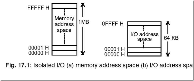
Ans. In isolated I/O scheme, memory and I/O are treated separately. The 1 MB address space can be treated as memory address space ranging from 00000 H to FFFFF H, while the address range from 00000 H to 0FFFF H (i.e., 64 KB I/O addresses) can be treated as I/O address space as shown below in Fig. 17.1.
It should be remembered that two consecutive memory or I/O addresses could be
accessed as a word-wide data.
4. Draw and explain the memory mapped I/O scheme for 8086.
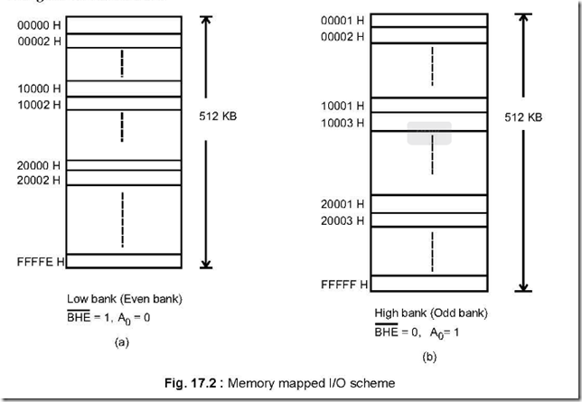
Ans. In this scheme, CPU looks to I/O ports as if it is part of memory. Some of the memory space is earmarked (dedicated) for I/O ports or addresses. The memory mapped I/O scheme is shown in Fig. 17.2 below in which the memory locations starting from C0000 H to C0FFF H (4 KB in all) and from D0000 H to D0FFF H (4 KB in all) are assigned to I/O devices.
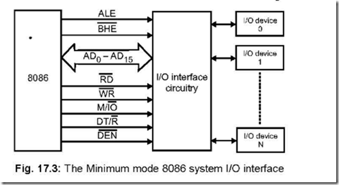
5. Draw the (a) MIN and (b) MAX mode 8086 based I/O interface. Ans. (a) The 8086 based Min mode I/O interface is shown below in Fig. 17.3.
It is seen that the lower two bytes AD0 – AD15 are used for input/output data transfers. The interface circuitry performs the following tasks.
z Selecting the particular I/O port
z Synchronise data transfer
z Latch the output data
z Sample the input data
z Voltage levels between the I/O devices and 8086 are made compatible.
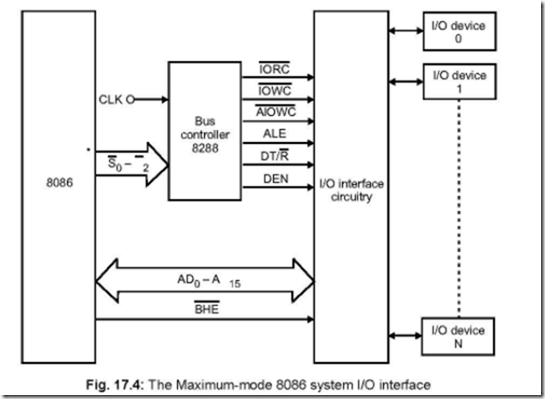
(b) The 8086 based Max mode I/O interface is shown below in Fig.17.4
![]()
![]() In this case the status codes S2 − S0 outputted by 8086 are fed to the 8288 bus controller IC. The decoder circuit within 8288 decodes these three signals. For nstance, 001 and 010 on S2 S1 S0 lines indicate ‘Read I/O port’ and ‘Write I/O port’ respectively. The first corresponds to IORC while the second corresponds to IOWC or AIOWC signals. These command signals are utilised to control data flow and its direction between I/O devices and the data bus.
In this case the status codes S2 − S0 outputted by 8086 are fed to the 8288 bus controller IC. The decoder circuit within 8288 decodes these three signals. For nstance, 001 and 010 on S2 S1 S0 lines indicate ‘Read I/O port’ and ‘Write I/O port’ respectively. The first corresponds to IORC while the second corresponds to IOWC or AIOWC signals. These command signals are utilised to control data flow and its direction between I/O devices and the data bus.
6. What kind of I/O is used for IN and OUT instructions?
Ans. For 8086 based systems, isolated I/O is used with IN and OUT instructions. The IN and OUT instructions are of two types: direct I/O instructions and variable I/O instructions. The different types of instructions are tabulated in Fig.17.5.
 Fig. 17.5: Input/output instructions
7. Which register(s) is/are involved in data transfers?
Ans. Only AL (for 8-bits) or AX (for16-bits) register is involved in data transfer involving the 8086’s CPU and I/O devices—thus they are also known as accumulator I/O.
8. Bring out the differences between direct I/O instructions and variable I/O instructions.
Ans. The differences between the two types of instructions are tabulated below in Table 17.2.
Table 17.2: Differences between direct and variable I/O instructions
|
Direct I/O |
Variable I/O |
|
1. Involves 8-bit address as part of instruction 2. Can access a maximum of 28 = 255 byte addresses. |
1. Involves 16-bit address as part of instruction. This resides in DX register. It must be borne in mind that the value in DX register is not an offset, but the actual port address. 2. Can access a maximum of 216 = 64 KB of addresses. |
9. Give one example each of (a) direct I/O (b) variable I/O instruction. Ans. (a) An example of direct I/O instruction is as follows:
IN AL, 0F2 H
On execution, the contents of the byte wide I/O port at address location F2 H will be put into AL register.
(b) An example of this type is:
MOV DX, 0C00F H IN AL, DX
On execution, at first DX register is loaded with the input port having address C00F H. The second instruction ensures that the port content is moved over to AL register.
10. Draw the (a) in port and (b) out port bus cycle of 8086.
Ans. (a) The input bus cycle of 8086 is shown in the Fig.17.6. In the first T state (i.e., T1), address comes out via A0–A19, along with BHE signal. Also ALE signal goes high in
T1. The high to low transition on ALE at the end of T1 latches the address bus. M/ IO
signal goes low at the beginning of T1. RD line goes low in T2 while data transfer
occurs in T3. DT/ R goes low at the beginning of T1 and DEN signal becomes active in T2 which tells the I/O interface circuit when to put data on the data bus.
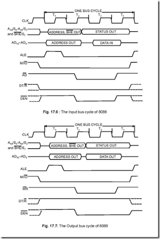 (b) The output bus cycle shown in Fig. 17.7.
The main differences between the output bus cycle and the just discussed input
bus cycle are:
![]()
![]() z WR Signal becomes active earlier than the RD signal. Hence in this case valid data is put on the data bus in T2 state.
z WR Signal becomes active earlier than the RD signal. Hence in this case valid data is put on the data bus in T2 state.
![]() z DEN signal becomes active in T1, while the same occurs in T2 state for input bus cycle.
z DEN signal becomes active in T1, while the same occurs in T2 state for input bus cycle.
