Microprogrammed Control Unit Design

Microprogrammed Control Unit Design

As mentioned earlier, a microprogramm d contwl unit contains programs written using microinstructions. These programs are stored in a control memory normally in a ROM inside the CPU. To execute instructions, the microprocessor reads (fetches) each instruction into the instruction register from external memory. The control unit translates the instruction for the microprocessor. Each control word contains signals to activate one or more microoperations. A program consisting of a set of microinstructions is executed in a sequence of micro-operations to complete the instruction execution. Generally, all microinstructions have two important fields:

  • Control word
  • Next address

The control field indicates which control lines are to be activated. The next address field specifies the address of the next microinstruction to be executed. The concept of microprogramming was first proposed by W. V. Wilkes in 1951 utilizing a decoder and an 8 x 8 ROM with a diode matrix. This concept is extended further to include a control memory inside the CPU. The cost of designing a CPU primarily depends on the size ofthe control memory. The length of a microinstruction, on the other hand, affects the size ofthe control memory. Therefore, a major design effort is to minimize the cost of implementing a microprogrammed CPU by reducing the length of the microinstruction.

The length of a microinstruction is directly related to the following factors:

  • The number of micro-operations that can be activated simultaneously. This is called the "degree of parallelism."
  • The method by which the address of the next microinstruction is determined.

All microinstructions executed in parallel can be included in a single microinstruction with a common op-code. The result is a short microprogram. However, the length of the microinstruction increases as parallelism grows.

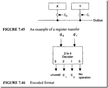
The control bits in a microinstruction can be organized in several ways. One obvious way is to assign a single bit for each control line. This will provide full parallelism. No decoding of the control field is necessary. For example, consider Figure 7.45 with two registers, X and Y with one outbus.

In figure 7.45, the contents of each register are transferred to the outbus when the

image


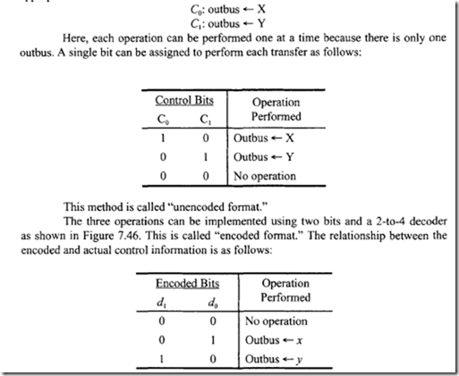
appropriate control line is activated:

image

Note that a 5-bit control field is required for five operations. However, three encoded bits are required for five operations using a 3 to 8 decoder. Hence, the encoded format typically provides a short control field and thus results in short microinstructions. However, the need for a decoder will increase the cost. Therefore, there is a trade-off between the degree of parallelism and the cost. Microinstructions can be classified into two groups: horizontal and vertical. The horizontal microinstruction mechanism provides long microinstructions, a high degree of parallelism, and little or no encoding. The vertical microinstruction method, on the other hand, offers short microinstructions, limited parallelism, and considerable decoding.

Microprogramming is the technique of wntmg microprograms in a microprogrammed control unit. Writing microprograms is similar to writing assembly language programs. Microprograms are basically written in a symbolic language called microassembly language. These programs are translated by a microassembler to generate microcodes, which are then stored in the control memory.

In the early days, the control memory was implemented using ROMs. However, these days control memories are realized in writeable memories. This provides the flexibility of interpreting different instruction set by rewriting the original microprogram, which allows implementation of different control units with the same hardware. Using this approach, one CPU can interpret the instruction set of another CPU. The design of a microprogrammed control unit is considered next. The 4-bit x 4-bit unsigned multiplication

image

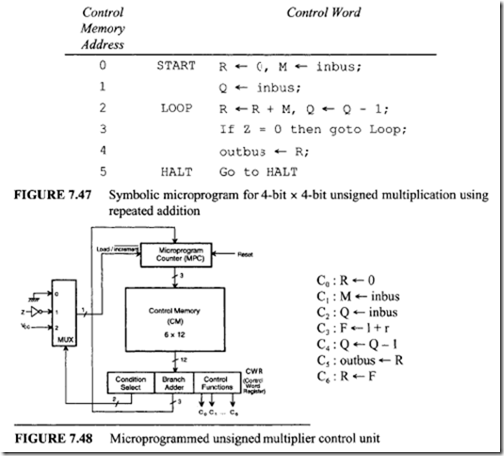
using hardwired control (presented earlier) is implemented by microprogramming. The register transfer description shown in Figure 7.36 is rewritten in symbolic microprogram language as shown in Figure 7.47. Note that the unsigned 4-bit x 4-bit multiplication uses repeated addition. The result (product) is assumed to be 4 bits wide.

To implement the microprogram, the hardware organization of the control unit

shown in Figure 7.48 can be used. The various components of the hardware of Figure 7.48 are described in the following:

1. Microprogram Counter (MPC). The MPC holds the address of the next microinstruction to be executed. It is initially loaded from an external source to point to the starting address of the microprogram. The MPC is similar to the program counter (PC). The MPC is incremented after each microinstruction fetch. If a branch instruction is encountered, the MPC is loaded with the contents of the branch address field of the microinstruction.

2. Control Word Register (CWR). Each control word in the control memory in this example is assumed to contain three fields: condition select, branch address, and control function. Each microinstruction fetched from the Control Memory is loaded into the CWR. The organization of the CWR is same for each control word and contains the three fields just mentioned. In the case of a conditional branch microinstruction, if the condition specified by the condition select field is true, the MPC is loaded with the branch address field of the CWR; otherwise, the MPC is incremented to point to the next microinstruction. The control function field contains the control signals.

3. MUX (Multiplexer). The MUX is a condition select multiplexer. It selects one

of the external conditions based on the contents of the condition select field of the microinstruction fetched into the CWR.

In Figure 7.48, a 2-bit condition select field is required as follows:

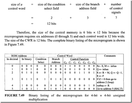
imageFrom Figure 7.47 six control memory address (addresses 0 through 5) are required for the control memory to store the microprogram. Therefore, a 3-bit address is necessary for each microinstruction. Hence, three bits for the branch address field are required. From Figure 7.48 seven control signals (C0 through C6) are required. Therefore, the size of the control function field is 7 bits wide. Thus, the size of each control word can be determined as follows:

image

Let us now explain the binary program. Consider the first line of the program. The instruction contains no branching. Therefore, the condition select field is 00. The contents of the branch in this case filled with 000. In the control function field, two micro­ operations, C0 and C1 , are activated. Therefore, both C0 and C1 are set to I; C2 through C6 are set to 0.

This results in the following binary microinstruction shown in the first line (address 0) of Figure 7.49:

imageNext, consider the conditional branch instruction of Figure 7.49. This microinstruction implements the conditional instruction "If Z = 0 then go to address 2." In this case, the microinstruction does not have to activate any control signal of the control function field. Therefore, C0 through C6 are zero. The condition select field is 01 because the condition is based on Z = 0. Also, if the condition is true (Z = 0), the program branches to address 2. Therefore, the branch address field contains 0102 • Thus, the following binary microinstruction is obtained:

image

The other lines in the binary representation of the microprogram can be explained similarly. To execute an unsigned multiplication instruction implemented using the repeated addition just described, a microprogrammed microprocessor will fetch the instruction from external memory into the instruction register. To execute this instruction, the microprocessor uses the control unit of Figure 7.48 to generate the control word based on the microprogram of Figure 7.49 stored in the control memory. The control signals C0 through C6 of the control function field of the CWR will be connected to appropriate components of Figure 7.38 The instruction will thus be executed by the microprocessor.

By examining the microprogram in Figure 7.49, it is obvious that the control function field contains all zeros in case of branch instructions. In a typical microprogram, there may be several conditional and unconditional branch instructions. Therefore, a lot of valuable memory space inside the control unit will be wasted if the control field is filled with zeros. In practice, the format of the control word is organized in a different manner to minimize its size. This reduces the implementation cost of the control unit. Whenever there are several branch instructions, the microinstructions, can be formatted by using a method called multiple microinstruction format. In this approach, the microinstructions are divided into two groups: operate and branch instructions.

An operate instruction initiates one or more microoperations. For example, after

the execution of an operate instruction, the MPC will be incremented by 1. In the case of a branch instruction, no microoperation will usually be initiated, and the MPC may be loaded with a new value. This means that the branch address field can be removed from the microinstruction format. Therefore, the control function field is used to specify the branch address itself. Typically,

image

If S1, S0 = 01, the instruction is regarded as a branch instruction, and the contents of the control field are assumed to be a 7-bit branch address. In this example, it is assumed that when S1, S0 = 01, the MPC will be loaded with the appropriate address specified by C6

C5 C4 C3 C2 C1, C0 if the condition ‘Z: = 0 is satisfied; on the other hand, if S1, S0 = 10, an

unconditional branch to the address specified by the Control Function I Branch Address

Field occurs.

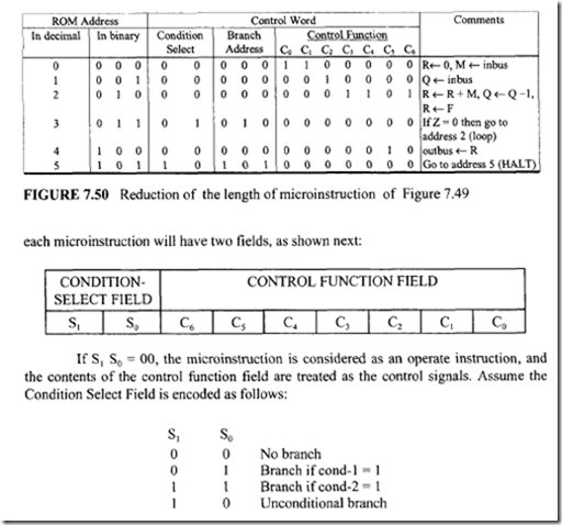
In order to illustrate this concept, the microprogram for 4-bit by 4-bit unsigned multiplication of Figure 7.49 is rewritten using the multiple instruction format as shown in Figure 7.50.

It can be seen from the figure 7.50 that the total size of the control store is 54 bits (6 x 9 = 54). In contrast, the control store of figure 7.49 contains 72 bits. For large microprograms with many branch instructions, tremendous memory savings can be accomplished using the multiple microinstructon format. Addresses 0, 1, 2, and 4 contain microinstructions with the contents of the conditional select field as 00, and are considered as operate instructions. In this case, the contents of the control function field are directed to the processing hardware.

Address 3 contains a conditional branch instruction since the contents of the condition select field are 01; while address 5 contains an unconditional branch instruction

image

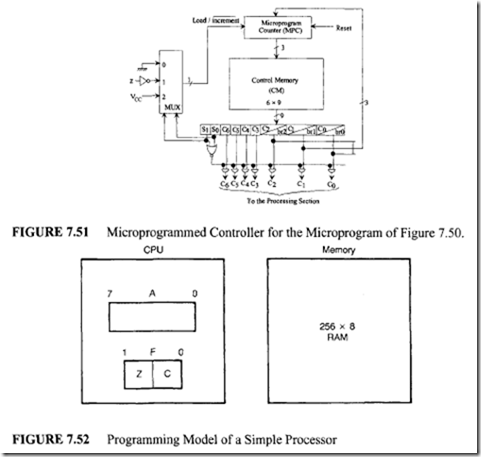
(halt instruction; that is, jump to the same address) since the condition select field is 10. Hence, the 7-bit control function field directly specifies the desired branch addresses 2 and 5, respectively. Figure 7.51 shows the hardware schematic.


Alu design , design of the control unit , basic concepts and hardwired control design

7.3.4 ALU Design

Functionally, an ALU can be divided up into two segments: the arithmetic unit and the logic unit. The arithmetic unit performs typical arithmetic operations such as addition, subtraction, and increment or decrement by 1. Usually, the operands involved may be signed or unsigned integers. In some cases, however, an arithmetic unit must handle 4-bit binary-coded decimal (BCD) numbers and floating-point numbers. Therefore, this unit must include the circuitry necessary to manipulate these data types. As the name implies, the logic unit contains hardware elements that perform typical operations such as Boolean NOT and OR. In this section, the design of a simple ALU using typical combinational elements such as gates, multiplexers, and a 4-bit parallel adder is discussed. For this approach, an arithmetic unit and a logic unit are first designed separately; then they are combined to obtain an ALU.

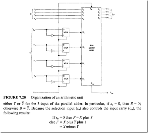
For the first step, a two-function arithmetic unit, as shown in Figure 7.20 is designed. The key element of this system is a 4-bit parallel adder. The multiplexers select

image

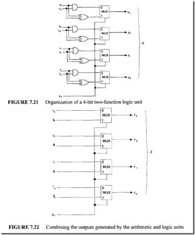
This arithmetic unit generates addition and subtraction operations. For the second step, let us design a two-function logic unit; this is shown in Figure 7.21. From Figure 7.21 it can be seen that when s0 = 0, the output G =X AND Y; otherwise the output G =X image Y. Note that from these two Boolean operations, other operations such as NOT and OR can be derived by the following Boolean identities:

1imagex = X

xORy =ximageyimagexy

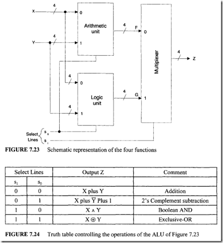
Therefore, NOT and OR operations can be obtained by using additional hardware and the circuit of Figure 7.21. The outputs generated by the arithmetic and logic units can be combined by using a set of multiplexers, as shown in Figure 7.22. From this organization it can be seen that when the select line s1 = 1, the multiplexers select outputs generated by the logic unit; otherwise, the outputs of the arithmetic unit are selected.

More commonly, the select line, s1, is referred to as the mode input because it selects the desired mode of operation (arithmetic or logic). A complete block diagram schematic of this ALU is shown in Figure 7.23. The truth table illustrating the operation of this ALU is shown in Figure 7.24. This table shows that this ALU is capable of performing 2 arithmetic and 2 logic operations on the 4-bit operands X and Y.

The rapid growth in IC technology permitted the manufacturers to produce an ALU as an MSI block. Such systems implement many operations, and their use as a system

image

component reduces the hardware cost, board space, debugging effort, and failure rate. Usually, each MSI ALU chip is designed as a 4-bit slice. However, a designer can easily interconnect n such chips to get a 4n-bit ALU. Some popular 4-bit ALU chips are the 74381 and 74181. The 74381 ALU performs 3 arithmetic and 2 miscellaneous operations on 4-bit operands. The 74181 ALU performs 16 arithmetic and 16 Boolean operations on two 4-bit operands, using either active high or active low data. A complete description and operational characteristics of these devices may be found in the data books.

Typical 8-bit microprocessors, such as the Intel 8085 and Motorola 6809, do not include multiplication and division instructions due to limitations in the circuit densities that can be placed on the chip. Due to advanced semiconductor technology, 16-, 32-, and 64-bit

 image

microprocessors usually include multiplication and division algorithms in a ROM inside the chip. These algorithms typically utilize an ALU to carry out the operations. Verilog and VHDL descriptions along with simulation results of typical ALU’s are included in Appendices I and J respectively.

7.3.5 Design of the Control Unit

The main purpose of the control unit is to translate or decode instructions and generate appropriate enable signals to accomplish the desired operation. Based on the contents of the instruction register, the control unit sends the selected data items to the appropriate processing hardware at the right time. The control unit drives the associated processing hardware by generating a set of signals that are synchronized with a master clock.

The control unit performs two basic operations: instruction interpretation and instruction sequencing. In the interpretation phase, the control unit reads (fetches) an instruction from the memory addressed by the contents of the program counter into the instruction register. The control unit inputs the contents of the instruction register. It recognizes the instruction type, obtains the necessary operands, and routes them to the appropriate functional units of the execution unit (registers and ALU). The control unit then issues the necessary signals to the execution unit to perform the desired operation and routes the results to the specified destination.

In the sequencing phase, the control unit generates the address of the next instruction to be executed and loads it into the program counter. To design a control unit, one must be familiar with some basic concepts such as register transfer operations, types of bus structures inside the control unit, and generation of timing signals. These are described in the next section.

There are two methods for designing a control unit: hardwired control and microprogrammed control. In the hardwired approach, synchronous sequential circuit design procedures are used in designing the control unit. Note that a control unit is a clocked sequential circuit. The name "hardwired control" evolved from the fact that the final circuit is built by physically connecting the components such as gates and flip-flops. In the microprogrammed approach, on the other hand, all control functions are stored in a ROM inside the control unit. This memory is called the "control memory." RAMs and PALs are also used to implement the control memory. The words in this memory are called "control words," and they specify the control functions to be performed by the control unit. The control words are fetched from the control memory and the bits are routed to appropriate functional units to enable various gates. An instruction is thus executed. Design of control units using microprogramming (sometimes calledfirmware to distinguish it froinhardwired control) is more expensive than using hardwired controls. To execute an instruction, the contents of the control memory in microprogrammed control must be read, which reduces the overall speed of the control unit.The most important advantage of microprogramming is its flexibility; many additions and changes are made by simply changing the microprogram in the control memory. A small change in the hardwired approach may lead to redesigning the entire system.

There are two types of microprocessor architectures: CISC (Complex Instruction Set Computer) and RISC (Reduced Instruction Set Computer). CISC microprocessors contain a large number of instructions and many addressing modes while RISC microprocessors include a simple instruction set with a few addressing modes. Almost all computations can be obtained from a few simple operations. RISC basically supports a small set of commonly used instructions which are executed at a fast clock rate compared to CISC which contains a large instruction set (some of which are rarely used) executed at a slower clock rate. In order to implement fetch /execute cycle for supporting a large instruction set for CISC, the clock is typically slower. In CISC, most instructions can access memory while RISC contains mostly load/store instructions. The complex instruction set of CISC requires a complex control unit, thus requiring microprogrammed implementation. RISC utilizes hardwired control which is faster. CISC is more difficult to pipeline while RISC provides more efficient pipelining. An advantage ofCISC over RISC is that complex programs require fewer instructions in CISC with a fewer fetch cycles while the RISC requires a large number of instructions to accomplish the same task with several fetch cycles. However, RISC can significantly improve its performance with a faster clock, more efficient pipelining and compiler optimization. PowerPC and Intel 80XXX utilize RISC and CISC architectures respectively. Intel Pentium family, on the other hand, utilizes a combination of RISC and CISC architectures for providing high performance. The Pentium uses RISC (hardwired control) to implement efficient pipelining for simple

imageinstructions. CISC (microprogrammed control) for complex instructions is utilized by the Pentium to provide upward compatibility with the Intel 8086/80X86 family.

Basic Concepts

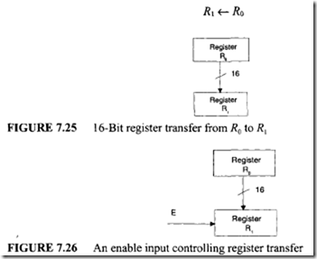
Register transfer notation is the fundamental concept associated with the control unit design. For example, consider the register transfer operation of Figure 7.25. The contents of 16-bit register R0 are transferred to 16-bit register R 1 as described by the following notation:

clip_image030_thumb

The symbol <— is called the transfer operator. However, this notation does not indicate the number of bits to be transferred. A declaration statement specifying the size of each register is used for the purpose:

Declare registers R0 [16],   R1    [16]

The register transfer notation can also be used to move a specific bit from one

register to a particular bit position in another. For example, the statement

R 1 [1] <— R0 [14]

means that bit 14 of register R0 is moved to bit I of register R 1

An enable signal usually controls transfer of data from one register to another.

For example, consider Figure 7.26. In the figure, the 16-bit contents of register R0 are transferred to register R 1 if the enable input E is HIGH; otherwise the contents of R0 and R 1 remain the same. Such a conditional transfer can be represented as

E: R 1 <— R0

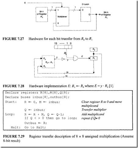
Figure 7.27 shows a hardware implementation of transfer of each bit of R0 and R 1

The enable input may sometimes be a function of more than one variable. For example,

consider the following statement involving three 16-bit registers: If R0 < R 1 and R2 [1] = I then R 1 <–R0

The condition R0 < R 1 can be determined by an 8-bit comparator such that the output y of the comparator goes to 0 if R0 < R 1 The conditional transfer can then be

image


expressed as follows: E: R1 <—- R0 where E= y ·R2 [1). Figure 7.28 depicts the hardware implementation.

A number of wires called "buses" are normally used to transfer data in and out of a digital processing system. Typically, there will be a pair of buses ("inbuses" and "outbuses") inside the CPU to transfer data from the external devises into the processing section and vice versa. Like the registers, these buses are also represented using register transfer notations and declaration statements. For example, "Declare inbus [16] and outbus [16]" indicate that the digital system contains two 16-bit wide data buses (inbus and outbus). R0 inbus means that the data on the inbus is transferred into register R0 when the next clock arrives. An equate(=) symbol can also be used in place of <— For example, "outbus = R 1 [15:8]" means that the high-order 8 bits of the 16-bit register R 1 are made available on the outbus for one clock period. An algorithm implemented by a digital system can be described by using a set of register transfer notations and typical control structures such as if-then and go to. For example, consider the description shown in Figure 7.29 for multiplying two 8-bit unsigned numbers (Multiplication of an 8-bit unsigned multiplier by an 8-bit multiplicand) using repeated addition.

The hardware components for the preceding description include an 8-bit inbus, an 8-bit outbus, an 8-bit parallel adder, and three 8-bit registers, R, M, and Q. This hardware performs unsigned multiplication by repeated addition. This is equivalent to unsigned multiplication performed by assembly language instruction.

A distinguishing feature of this description is to describe concurrent operations. For example, the operations R <— 0 and M <— inbus can be performed simultaneously. As a general rule, a comma is inserted between operations that can be executed concurrently. On the other hand, a semicolon between two transfer operations indicates that they must be performed serially. This restriction is primarily due to the data path provided in the hardware. For example, in the description, because there is only one input bus, the operations M

inbus and Q <— inbus cannot be performed simultaneously. Rather, these two operations must be carried out serially. However, one of these operations may be overlapped with the operation R <— 0 because the operation does not use the inbus. The description also includes labels and comments to improve readability of the task description. Operations such as R <—0 and M <— inbus are called "micro-operations", because they can be completed in one clock cycle. In general, a computer instruction can be expressed as a sequence of micro­ operations.

The rate at which a microprocessor completes operations such as R<—R + M is determined by its bus structure inside the microprocessor chip. The cost of the microprocessor increases with the complexity of the bus structure. Three types of bus

structures are typically used: single-bus, two-bus, and three-bus architectures.

The simplest of all bus structures is the single-bus organization shown in Figure 7.30. At any time, data may be transferred between any two registers or between a register and the ALU. If the ALU requires two operands such as in response to an ADD instruction, the operands can only be transferred one at a time. In single-bus architecture, the bus must be multiplexed among various operands. Also, the ALU must have buffer registers to hold the transferred operand.

In Figure 7.30, an add operation such as R0 <— R 1 + R2 is completed in three clock cycles as follows:

  • First clock cycle: The contents of R 1 are moved to buffer register B 1 of the ALU. Second
  • clock cycle: The contents of R2 are moved to buffer register B2 of the ALU.
  • Third clock cycle: The sum generated by the ALU is loaded into R0

A single-bus structure slows down the speed of instruction execution even though data may already be in the microprocessor registers. The instruction’s execution time is longer if the operands are in memory; two clock cycles may be required to retrieve the operands into the microprocessor registers from external memory.

image_thumb

To execute an instruction such as ADD between two operands already in register, the control logic in a single-bus structure must follow a three-step sequence. Each step represents a control state. Therefore, a single-bus architecture requires a large number of states in the control logic, so more hardware may be needed to design the control unit. Because all data transfers take place through the same bus one at a time, the design effort to build the control logic is greatly reduced.

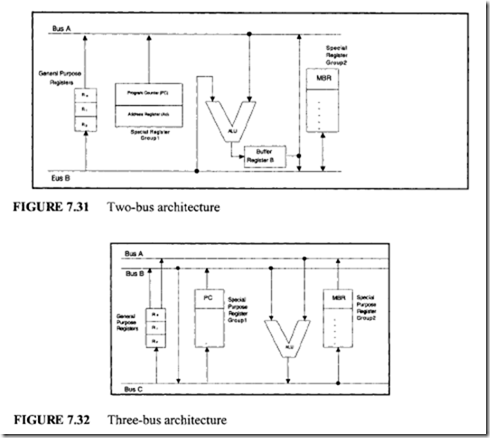
Next, consider a two-bus architecture, shown in Figure 7.31. All general-purpose registers are connected to both buses (bus A and bus B) to form a two-bus architecture. The two operands required by the ALU are, therefore, routed in one clock cycle. Instruction execution is faster because the ALU does not have to wait for the second operand, unlike the single-bus architecture. The information on a bus may be from a general-purpose register or a special-purpose register. In this arrangement, special-purpose registers are often divided into two groups. Each group is connected to one of the buses. Data from two special-purpose registers of the same group cannot be transferred to the ALU at the same time.

In the two-bus architecture, the contents of the program counter are always transferred to the right input of the ALU because it is connected to bus A. Similarly, the contents of the special register MBR (memory buffer register, to hold up data retrieved from external memory) are always transferred to the left input of the ALU because it is connected to bus B.

In Figure 7.31, an add operation such as R0 o(- R 1 + R2 is completed in two clock cycles as follows:

  • First clock cycle: Second clock cycle: The contents of R 1 and R2 are moved to the inputs of ALU.
  • The ALU then generates the sum in the output register. The sum from the output register is routed to R0

The performance of a two-bus architecture can be improved by adding a third bus (bus C), at the output of the ALU. Figure 7.32 depicts a typical three-bus architecture. The three-bus architecture perform the addition operation R0 o(- R 1 + R2 in one cycle as follows:

  • First cycle: The contents of R 1 and R2 are moved to the inputs of the ALU via bus A and bus B respectively. The sum generated by the ALU is then transferred to R0 via bus C.

The addition of the third bus will increase the system cost and also the complexity of the control unit design.

Note that the bus architectures described so far are inside the microprocessor chip. On the other hand, the system bus connecting the microprocessor, memory, and I/O are external to the microprocessor.

Another important concept required in the design of a control unit is the generation of timing signals. One of the main tasks of a control unit is to properly sequence a set of operations such as a sequence of n consecutive clock pulses. To carry out an operation, timing signals are generated from a master clock. Figure 7.33 shows the input clock pulse and the four timing signals T0, T1 , T2 , and T3 A ring counter (described in Chapter 5) can be used to generate these timing signals. To carry out an operation Pi at the ith clock pulse, a control unit must count the clock pulses and produce a timing signal Ti.

Hardwired Control Design

The steps involved in hardwired control design are summarized as follows:

1. Derive a flowchart from the problem definition and validate the algorithm by using trial data.

2. Obtain a register transfer description of the algorithm from the flowchart.

3. Specify a processing hardware along with various components.

4. Complete the design of the processing section by establishing the necessary control inputs.

5. Determine a block diagram of the controller.

image_thumb[1]

6. Obtain the state diagram of the controller.

7. Specify the characteristic of the hardware for generating the required timing signals used in the controller.

8. Draw the logic circuit of the controller.

The following example is provided to illustrate the concepts associated with implementation of a typical instruction in a control unit using hardwired control. The unsigned multiplication by repeated addition discussed earlier is used for this purpose. A 4-

image_thumb[2]

bit by 4-bit unsigned multiplication will be considered. Assume the result of multiplication is 4 bits.

Step 1: Derive a flowchart from the problem definition and then validate the algorithm using trial data.

Figure 7.34 shows the flowchart. In the figure, M and Q are two 4-bit registers containing the unsigned multiplicand and unsigned multiplier respectively. Assume that the result of multiplication is 4-bit wide. The 4-bit result of the multiplication called the "product" will be stored in the 4-bit register, R. The contents of R are then output to the outbus.

The flowchart in Figure 7.34 is similar to an ASM chart and provides a hardware description of the algorithm. The sequence of events and their timing relationships are described in the flowchart. For example, the operations, R E <— 0 and M <— multiplicand shown in the same block are executed simultaneously. Note that M <— multiplicand via inbus and Q <— multiplier via inbus must be performed serially because both operations use a single input bus for loading data. These operations are, therefore, shown in different

image_thumb[3]

blocks. Because R<— 0 does not use the inbus, this operation is overlapped, in our case, with initializing of M via the inbus. This simultaneous operation is indicated by placing them in the same block.

The algorithm will now be verified by means of a numerical example as shown in Figure 7.35. Suppose M = 01002 = 410 and Q = 00112 = 310; then R =product= 11002 = 1210

Step 2: Obtain a register transfer description of the algorithm from the flowchart. Figure 7.36 shows the description of the algorithm.

Step 3: Specify a processing hardware along with various components. The processing section contains three main components:

  • General-purpose registers
  • 4-bit adder
  • Tristate buffer

Figure 7.37 shows these components. The general-purpose register is a trailing edge-triggered device.

Three operations (clear, parallel load, and decrement) can be performed by applying the appropriate inputs at C, L, and D. All these operations are synchronized at the trailing (high to low) edge of the clock pulse.

The 4-bit adder can be implemented using 4-bit adder circuits. The tristate buffer is used to control data transfer to the outbus.

Step 4: Complete the design of the processing section by establishing the necessary control inputs.

Figure 7.38 shows the detailed logic diagram of the processing section, along with the control inputs.

Step 5: Determine a block diagram of the controller. Figure 7.39 shows the block diagram.

The controller has three inputs and seven outputs. The Reset input is an asynchronous input used to reset the controller so that a new computation can begin. The Clock input is used to synchronize the controller’s action. All activities are assumed to be synchronized with the trailing edge of the clock pulse.

Step 6: Obtain the state diagram of the controller.

The controller must initiate a set of operations in a specified sequence. Therefore, it is modeled as a sequential circuit. The state diagram of the unsigned multiplier controller is shown in Figure 7.40.

Initially, the controller is in state T0 At this point, the control signals C0 and C1 are HIGH. Operations R 0 and M inbus are carried out with the trailing edge of the next clock pulse. The controller moves to state T1 with this clock pulse. When the controller is

in T2, R <— R + M and Q <— Q – 1 are performed.

All these operations take place at the trailing edge of the next clock pulse. The controller moves to state T5 only when the unsigned multiplication is completed. The controller then stays in this state forever. A hardware reset input causes the controller to move to state T0, and a new computation will start.

In this state diagram, selection of states is made according to the following guidelines:

If the operations are independent of each other and can be completed within one clock cycle, they are grouped within one control state. For example, in Figure 7.40, operations R 0 and M ,. inbus are independent of each other. With this hardware, they can be executed in one clock cycle. That is, they are

image_thumb[4]

image_thumb[5]

image_thumb[6]

microoperations. However, if they cannot be completed within the T0 clock cycle, either clock duration must be increased or the operations should be divided into a sequence of microoperations.

  • Conditional testing normally implies the introduction of new states. For example, in the figure, conditional testing of Z introduces the new state T3
  • One should not attempt to minimize the number of states. When in doubt, new states must be introduced. The correctness of the control logic is more important than the cost of the circuit.

Step 7: Specify the characteristics of the hardware for generating the required timing signals.

There are six states in the controller state diagram. Six nonoverlapping timing signals (T0 through T5) must be generated so that only one will be high for a clock pulse. For example, Figure 7.41 shows the four timing signals T0, T1, T2,and T3 A mod-8 counter and a 3-to-8 decoder can be used to accomplish this task. Figure 7.42 shows the mod-8 counter.

Step 8: Draw the logic circuit of the controller.

Figure 7.43 shows the logic circuit of the controller. The key element of the implementation in Figure 7.43 is the sequence controller (SC) hardware, which sequences

image_thumb[7]

image_thumb[8]

image_thumb[9]the controller according to the state diagram of Figure 7.40. Figure 7.44(a) shows the truth table for the SC controller.

Consider the logic involved in deriving the entries of the SC truth table. The mod- 8 counter is loaded (or initialized) with the specified external data if the counter control inputs C and L are 0 and I respectively from Figure 7.42. In this counter, the counter load control input L overrides the counter enable control input E.

From the controller’s state diagram of Figure 7.40, the controller counts up automatically in response to the next clock pulse when the counter load control input L = 0 because the enable input E is tied to HIGH. Such normal sequencing activity is desirable for the following situations:

  • Present control state is T0, T1 , T2, T4
  • Present control state is T3 and Z = 1; the next state is T4
  • The SC must load the counter with the appropriate count when the counter is required to load the count out of its normal sequence.

For example, from the controller’s state diagram of Figure 7.40, if the present control state is T3 (counter output O2O1O0= 011) and if Z = 0, the next state is T2• When these input conditions occur, the counter must be loaded with external value 010 at the trailing edge of the next clock pulse (T2 = I only when O2O1O0= 010. Therefore, the SC generates L = 1 and d2d1d0= 010.

Similarly, from the controller’s state diagram of Figure 7.40, if the present state is T5 , the next control state is also T5 The SC must generate the outputs L = 1 and dAdo = 101. The SC truth table of Figure 7.41 shows these out-of-sequence counts. For each row of the SC truth table of Figure 7.44(a), a product term is generated in the PLA:

P0 + ZT3 and P, = T5

The PLA (Figure 7.44b) generates four outputs: L, d2, d,, and d0Each output is directly generated by the SC truth table and the product terms. The PLA outputs are as follows: image_thumb[10]

From these equations, when the control is in state T0 or T2 , multiple micro­ operations are performed. Otherwise,when the control is in state T, or T4, a single micro­ operation is performed.

The unsigned multiplication algorithm just implemented using hardwired control can be considered as an unsigned multiplication instruction with a microprocessor. To execute this instruction, the microcomputer will read (fetch) this multiplication instruction from external memory into the instruction register located inside the microprocessor. The contents of this instruction register will be input to the control unit for execution. The control unit will generate the control signals C0 through C6 as shown in Figure 7.43. These control signals will then be applied to the appropriate components of the processing section in Figure 7.38 at the proper instants of time shown in Figure 7.40. Note that the control signals are physically connected to the hardware elements of Figure 7.38. Thus, the execution of the unsigned multiplication instruction will be completed by the microprocessor.


Design of computer instruction set and the cpu : desi n of the cpu ,register design and adders

7.1 Desi n of the CPU

The CPU contains three elements: registers, the ALU (Arithmetic Logic Unit), and the control unit. These topics are discussed next. Verilog and VHDL descriptions along with simulation results of a typical CPU are provided in Appendices I and J respectively.

7.3.1 Register Design

The concept of general-purpose and flag registers is provided in Chapters 5 and 6. The main purpose of a general-purpose register is to store address or data for an indefinite period of time. The computer can execute an instruction to retrieve the contents of this register when needed. A computer can also execute instructions to perform shift operations on the contents of a general-purpose register. This section includes combinational shifter design and the concepts associated with barrel shifters.

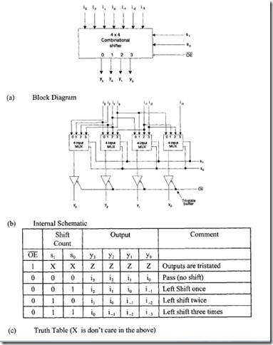
A high-speed shifter can be designed using combinational circuit components such as a multiplexer. The block diagram, internal organization, and truth table of a typical combinational shifter are shown in Figure 7.7. From the truth table, the following equations can be obtained:

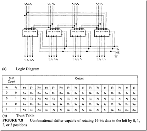
imageThe 4 x 4 shifter of Figure 7.7 can be expanded to obtain a system capable of rotating 16-bit data to the left by 0, 1, 2, or 3 positions, which is shown in Figure 7.8.

This design can be extended to obtain a more powerful shifter called the barrel

image

FIGURE7.7 4 x 4 combinational shifter

shifter. The shift is a cycle rotation, which means that the input binary information is shifted in one direction; the most significant bit is moved to the least significant position.

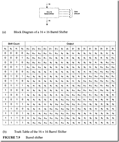
The block-diagram representation of a 16 x 16 barrel shifter is shown in Figure 7.9. This shifter is capable of rotating the given 16-bit data to the left by n positions, where 0 s n s 15. Figure 7.9 shows the truth table representing the operation of the shifter. The barrel shifter is an on-chip component for typical 32-bit and 64-bit microprocessors.

image7.3.2 Adders

Addition is the basic arithmetic operation performed by an ALU. Other operations such as subtraction and multiplication can be obtained via addition. Thus, the time required to add two numbers plays an important role in determining the speed of the ALU.

The basic concepts of half-adder, full adder, and binary adder are discussed in Section 4.5 .1. The following equations for the full-adder were obtained. Assume xi = x, yi

image

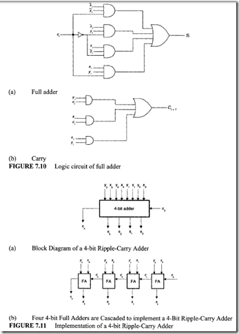
The logic diagrams for implementing these equations are given in Figure 7.10.

As has been made apparent by Figure 7.10, for generating Ci+I from ci, two gate delays are required. To generate Si from ci, three gate delays are required because ci must be inverted to obtain ci. Note that no inverters are required to get X: or .Y; from xi or yi, respectively, because the numbers to be added are usually stored in a register that is a collection of flip-flops. The flip-flop generates both normal and complemented outputs.

image

For the purpose of discussion, assume that the gate delay is ll. time units, and the actual value of ll. is decided by the technology. For example, if transistor translator logic (TTL) circuits are used, the value of ll. will be 10 ns.

By cascading n full adders, an n-bit binary adder capable of handling two n-bit operands (X and Y) can be designed. The implementation of a 4-bit ripple-carry or binary adder is shown in Figure 7.11. When two unsigned integers are added, the input carry, c0, is always zero. The 4-bit adder is also called a "carry-propagate adder" (CPA), because the carry is propagated serially through each full adder. This hardware can be cascaded to obtain a 16-bit CPA, as shown in Figure 7.12; c0 = 0 or 1 for multiprecision addition.

Although the design of an n-bit CPA is straightforward, the carry propagation

time limits the speed of operation. For example, in the 16-bit CPA (see Figure 7.12), the

imageaddition operation is completed only when the sum bits s0 through s15 are available.

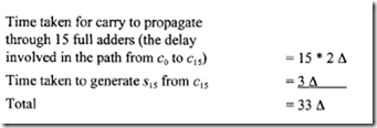
To generate s15, c15 must be available. The generation of c15 depends on the availability of c 14, which must wait for c13 to become available. In the worst case, the carry process propagates through 15 full adders. Therefore, the worst-case add-time of the 16-bit CPA can be estimated as follows:


clip_image024

FIGURE 7.12 Implementation of a 16-bit adder using 4-Bit Adders as Building Blocks

image

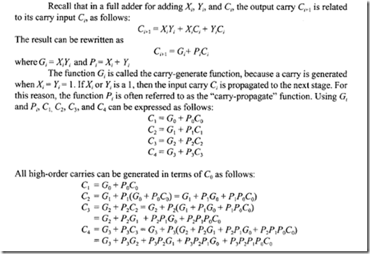
If Δ = 10 ns, then the worst-case add-time of a 16-bit CPA is 330 ns. This delay is prohibitive for high-speed systems, in which the expected add-time is typically less than 100 ns, which makes it necessary to devise a new technique to increase the speed of operation by a factor of 3. One such technique is known as the "carry look-ahead." In this approach the extra hardware is used to generate each carry (c;, i > 0) directly from c0To be more practical, consider the design of a 4-bit carry look-ahead adder (CLA). Let us see how this may be used to obtain a 16-bit adder that operates at a speed higher than the 16-bit CPA.

image

image

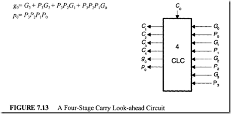
Therefore C1 , C2 , C3, and C4 can be generated directly from C0 • For this reason, these equations are called "carry look-ahead equations," and the hardware that implements these equations is called a "4-stage look-ahead circuit" (4-CLC). The block diagram of such circuit is shown in Figure 7.13.

The following are some important points about this system:

  • A 4-CLC can be implemented as a two-level AND-OR logic circuit (The first level consists of AND gates, whereas the second level includes OR gates).
  • The outputs g0 and p 0 are useful to obtain a higher-order look-ahead system.

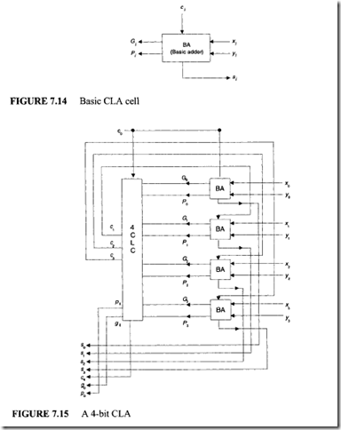
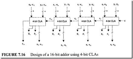
To construct a 4-bit CLA, assume the existence of the basic adder cell shown in Figure 7.14. Using this basic cell and 4-bit CLC, the design of a 4-bit CLA can be completed as shown in Figure 7.15. Using this cell as a building block, a 16-bit adder can be designed as shown in Figure 7.16.

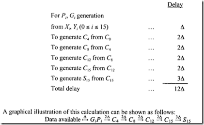
The worst-case add-time of this adder can be calculated as follows:

image

From this calculation, it is apparent that the new I 6-bit adder is faster than the 16-bit CPA by a factor of 3. In fact, this system can be speeded up further by employing another 4-bit CLC and eliminating the carry propagation between the 4-bit CLA blocks. For this purpose, the gi and Pi outputs generated by the 4-bit CLA are used. This design task is left as an exercise to the reader.

image


image


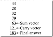
If there is a need to add more than 3 operands, a technique known as "carry-save addition" is used. To see its effectiveness, consider the following example:

image

In this example, four decimal numbers are added. First, the unit digits are added, producing a sum of3 and a carry digit of2. Similarly, the tens digits are added, producing a sum digit of 6 and a carry digit of 1. Because there is no carry propagation from the unit digit to the tenth digit, these summations can be carried out in parallel to produce a sum vector of 63 and a carry vector of 12. When all operands are exhausted, the sum and the shifted carry vector are added in the conventional manner, which produces the final answer. Note that the carry is propagated only in the last step, which generates the final answer no matter how many operands are added. The concept is also referred to as "addition by deferred carry assimilation."


Addition, Subtraction, Multiplication and Division of unsigned and signed numbers

7.3.3 Addition, Subtraction, Multiplication and Division of unsigned and signed numbers

The procedure for addition and subtraction of two’s complement signed binary numbers

is straightforward. The procedure for adding unsigned numbers is discussed in Chapter

2. Also, addition of two 2’s complement signed numbers was included in Chapter 2. Note that binary numbers represented in two’s complement form contain both unsigned numbers (Most Significant Bit= 0) and signed numbers (Most Significant Bit= 1). The procedure for adding two 2’s complement signed numbers using pencil and paper is provided below:

Add the two numbers along with the sign bits. Check the overflow bit (V) using V = Cr 81 Cp where Cr is the final carry and CP is the previous carry. If V = 0, then the result of addition is correct. On the other hand, if V = 1, then the result is incorrect; one needs to increase the number of bits for each number, and repeat the addition operation until V = 0 to obtain the correct result.

Subtraction of two 2’s complement signed binary numbers using pencil and paper can be performed as follows:

Take the 2’s complement of subtrahend along with the sign bit and add it to the minuend . The result is correct if there is no overflow. The result is wrong if there is an overflow. In case of overflow, increase the number of bits for each number, repeat the subtraction operation until the overflow is zero to obtain the correct result. Note that if there is a final carry after performing the 2’s complement subtraction, the result is positive. On the other hand, if there is no final carry after 2’s complement subtraction, the result is negative.

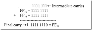
Computers utilize common hardware to perform addition and subtraction operations for both unsigned and signed numbers. The instruction set of computers typically include the same ADD and SUBTRACT instructions for both unsigned and signed numbers. The interpretations of unsigned and signed ADD and SUBTRACT operations are performed by the programmer. For example, consider adding two 8-bit numbers, A and B (A= FF 16 and B= FF 16 ) using the ADD instruction by a computer as follows:

imageWhen the above addition is interpreted as an unsigned operation by the programmer, the result will be

A+ B =FF 16 + FF16 = 25510+ 255 10= 51010 which is FE16 with a carry as shown above. However, if the addition is interpreted as a signed operation, then, A+ B =FF 16 + FF16 = (-110) + (-110) = -210 which is FE16 as shown above, and the final carry must be discarded by the programmer. Similarly, the unsigned and signed subtraction can be interpreted by the programmer.

Typical 8-bit microprocessors, such as the Intel 8085 and Motorola 6809, do not include multiplication and division instructions due to limitations in the circuit densities that can be placed on the chip. Due to advances in semiconductor technology, 16-, 32-, and 64-bit microprocessors usually include multiplication and division algorithms in a ROM inside the chip. These algorithms typically utilize an ALU to carry out the operations. one can write a program that multiplies two numbers. Although this solution seems viable, the operational speed is unsatisfactory.

For application environments such as real-time digital filtering, in which the processor is expected to perform 32 to 64 eight-bit multiplication operations within 100

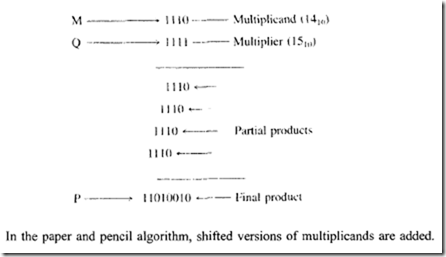
!!Sec (sampling frequency= 10kHz), speed is an important factor. New device technologies such as BICMOS and HCMOS, allow manufacturers to pack millions of transistors in a chip. Consequently, state-of-the-art 32-bit microprocessors such as the Motorola 68060 (HCMOS) and Intel Pentium (BICMOS) designed using these technologies, have a larger instruction set than their predecessors, which includes multiplication and division instructions. In this section, multiplier design principles are discussed. Two unsigned integers can be multiplied using repeated addition as mentioned in Chapter 2. Also, they can be multiplied in the same way as two decimal numbers are multiplied by paper and pencil method. Consider the multiplication of two unsigned integers, where the multiplier Q = 15 and the multiplicand is M = 14, as illustrated:

image

image

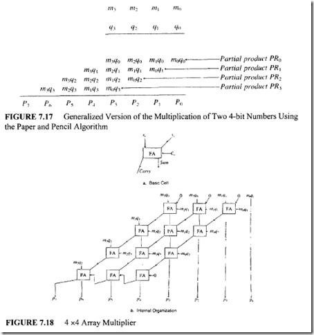
This procedure can be implemented by using combinational circuit elements such as AND gates and FULL adders. Generally, a 4-bit unsigned multiplier Q and a 4-bit unsigned multiplicand M can be written as M: m3 m2 m 1 m0 and Q: q3 q2 q1 q0.The process of generating the partial products and the final product can also be generalized as shown in

image

Figure 7.17. Each cross-product term (mi q) in this figure can be generated using an AND gate. This requires 16 AND gates to generate all cross-product terms that are summed by full adder arrays, as shown in Figure 7.18.

Consider the generation of p 2 in Figure 7.18(b). From Figure 7.17, p 2 is the sum of m2q0, m1 q1 and m0q2 The sum of these three elements is obtained by using two full adders. (See column for p 2 in Figure 7.18). The top full-adder in this column generates the sum m2q0 + m1q 1 This sum is then added to m0q2 by the bottom full-adder along with any carry from the previous full-adder for p 1

The time required to complete the multiplication can be estimated by considering the longest carry propagation path comprising of the rightmost diagonal (which includes the full-adder for p 1 and the bottom full-adders for p2 and p3 ), and the last row (which includes the full-adder for p6 and the bottom full-adders for p4 and p5). The time taken to multiply  two n-bit numbers can be expressed as follows:

imageIn this equation, all cross-product terms miqi can be generated simultaneously by an array of AND gates. Therefore, only one AND gate delay is included in the equation. Also, the rightmost diagonal and the bottom row contain (n – 1) full-adders each for the n x n multiplier.

Assuming that image   be simplified as shown:

T(n) = 2 Δ+ (2n- 2)2Δ = (4n- 2)Δ .

The array multiplier that has been considered so far is known as Braun’s multiplier. The hardware is often called a nonadditive multiplier (NM), since it does not include any additive inputs. An additive multiplier (AM) includes an extra input R; it computes products of the form

P=M*Q+R

This type of multiplier is useful in computing the sum of products of the form };XiYi. Both an NM and an AM are available as standard 1C blocks. Since these systems require more components, they are available only to handle 4- or 8-bit operands.

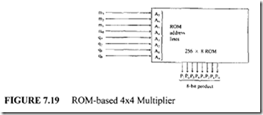
Alternatively, the same 4×4 NM discussed earlier can be obtained using a 256 x 8 ROM as shown in Figure 7.19.

It can be seen that a given MQ pair defines a ROM address, where the corresponding 8-bit product is held. The ROM approach can be used for small-scale multipliers because:

  • The technological advancements allow the manufacturers to produce low-cost ROMs.
  •  The design effort is minimum.

In case of large multipliers, ROM implementation is unfeasible, since large-size ROMs are required. For example, in order to implement an 8 x 8 multiplier, a 216 x 16 ROM is required. If the required 8 x 8 product is decomposed into a linear combination offour 4×4 products, an 8 x 8 multiplier can be implemented using four 256 x 8 ROMs and a few 4-bit parallel adders. However, PLDs can be used to accomplish this.Signed multiplication can be performed using various algorithms. A simple algorithm follows.

  • In the case of signed numbers, there are three possibilities:

I. M and Q are in sign-magnitude form.

2. M and Q are in ones complement form.

3. M and Q are in twos complement form.

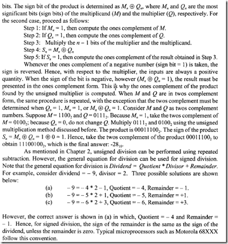
For the first case, perform unsigned multiplication of the magnitudes without the sign

image


DESIGN OF COMPUTER INSTRUCTION SET ANDTHECPU: Design of the Computer Instructions and Reduced Instruction Set Computer (RISC)

clip_image001DESIGN OF COMPUTER INSTRUCTION SET ANDTHECPU

This chapter describes the design of the instruction set and the central processor unit (CPU). Topics include op-code encoding, design of typical microprocessor registers, the arithmetic logic unit (ALU), and the control unit.

7.1 Design of the Computer Instructions

A program consists of a sequence of instructions. An instruction performs operations on stored data. There are two components in an instruction: an op-code field and an address field. The op-code field defines the type of operation to be performed on data, which may be stored in a microprocessor register or in the main memory. The address field may contain one or more addresses of data. When data are read from or stored into two or more addresses by the instruction, the address field may contain more than one address. For example, consider the following instruction:

image

Assume that this computer uses DO as the source register and D 1 as the destination register. This instruction moves the contents of the microprocessor register DO to register D 1. The number and types of instructions supported by a microprocessor vary from one microprocessor to another and primarily depend on the microprocessor architecture. The number of instructions supported by a typical microprocessor depends on the size of the op-code field. For example, an 8-bit op-code can specify a maximum of 256 unique instructions.

As mentioned before, a computer only understands 1’sand O’s. This means that the computer can execute an instruction only if it is in binary. A unique binary pattern must be assigned to each op-code by a process called "op-code encoding."

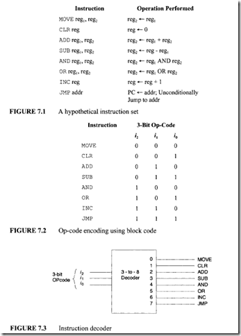
The Block code method is one of the simplest techniques of designing instructions. In this approach, a fixed length ofbinary pattern is assigned to each op-code. For example, an n-bit binary number can represent 2" unique op-codes. Consider for example, a hypothetical instruction set shown in Figure 7.1. In this figure, there are 8 different instructions that can be encoded using three bitsi2,i1 i0 as shown in Figure 7.2. A 3-to-8 decoder can be used to encode the 8 hypothetical instructions as shown in Figure 7.3.

An n-to-2" decoder is required for ann-bit op-code. As n increases, the cost of the decoder and decoding time will also increase. In some op-code encoding techniques such as the "expanding op-code" method, the length of the instruction is a function of the number of addresses used by the instruction. For example, consider a 16-bit instruction in which the lengths of the op-code and address fields are 5 bits and 11 bits respectively. Using such an instruction format, 32 (25) operations allowing access to 2048 (211memory locations an be specified. Now, if the size of the instruction is kept at 16 bits but the address field is increased to 12 bits, the op-code length will then be decreased to 4 bits. This change will specify 16 (24) operations with access to 4096 (212) memory locations. Thus, the number of

image

operations is reduced by 50% and the number of memory locations is increased by 100%. This concept is used in designing instructions with expanding op-code technique.

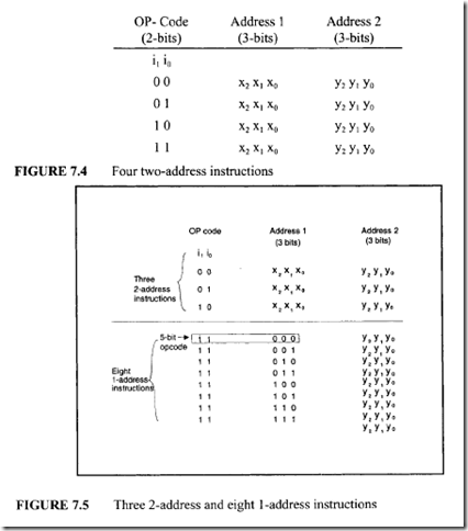
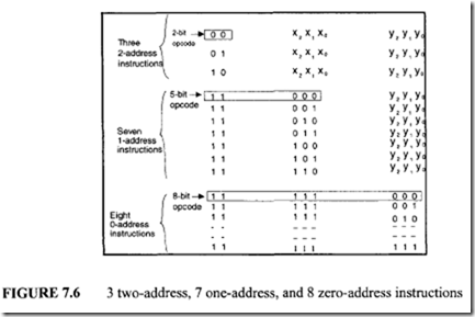
Consider an instruction format with 8-bit instruction length and a 2-bit op-code field. Four unique two-address (3 bits for each address) instructions can be specified. This is depicted in Figure 7.4. If three rather than four two-address instructions are used, eight one-address instructions can be specified. This is shown in Figure 7.5. The length of the op-code field for each one-address instruction is 5 bits. Thus, the length of the op-code field increases as the number of address field is decreased. Now, if the total number of one-address instructions is reduced from 8 to 7, then eight 0-address instructions can also be specified. This is shown in Figure 7.6.

7.2 Reduced Instruction Set Computer (RISC)

RISC, which stands for reduced instruction set computer, is a generation of faster and inexpensive machines. The initial application of RISC principles has been in desktop workstations. Note that the PowerPC is a RISC microprocessor. The basic idea behind

image

image

RISC is for machines to cost less yet run faster, by using a small set of simple instructions for their operations. Also, RISC allows a balance between hardware and software based on functions to be achieved to make a program run faster and more efficiently. The philosophy of RISC is based on six principles: reliance on optimizing compilers, few instructions and addressing modes, fixed instruction format, instructions executed in one machine cycle, only call/return instructions accessing memory, and hardwired control.

The trend has always been to build CISCs (complex instruction set computers),

which use many detailed instructions. However, because of their complexity, more hardware would have to be used. The more instructions, the more hardware logic is needed to implement and support them. For example, in a RISC machine, an ADD instruction takes its data from registers. On a CISC, each operand can be stored in any of many different forms, so the compiler must check several possibilities. Thus, both RISC and CISC have advantages and disadvantages. However, the principles of understanding optimizing compilers and what actually happens when a program is executed lead to RISC.

Case Study: RISC I (University of California, Berkeley)

The RISC machine presented in this section is the one investigated at the University of California, Berkeley. The RISC I is designed with the following design constraints:

1. Only one instruction is executed per cycle.

2. All instructions have the same size.

3. Only load and store instructions can access memory.

4. High-level languages (HLL) are supported.

Two high level Languages (C and Pascal) were supported by RISC I. A simple architecture implies a fewer transistors, and this leads to the fact that most pieces of a RISC HLL system are in software. Hardware is utilized for time-consuming operations. Using C and Pascal, a comparison study was made to determine the frequency of occurrence of particular variable and statement types. Studies revealed that integer constants appeared most frequently, and a study of the code produced revealed that the procedure calls are the most time-consuming operations.

i) Basic RISC Architecture

The RISC I instruction set contains a few simple operations (arithmetic, logical, and shift). These instructions operate on registers. Instruction, data, addresses and registers are all 32 bits long. RISC instructions fall in four categories: ALU, memory access, branch, and miscellaneous. The execution time is given by the time taken to read a register, perform an ALU operation, and store the result in a register. Register 0 always contains a 0. Load and store instructions move data between registers and memory. These instructions use two CPU cycles. Variations of memory-access instructions exist in order to accommodate sign-extended or zero-extended 8-bit, 16-bit and 32-bit data. Though absolute and register indirect addressing are not directly available, they may be synthesized using register 0. Branch instructions include CALL, RETURN, and conditional and unconditional jumps. The following instruction format is used:

image

For register-to-register instructions, dest selects one of the 32 registers as destination of the result of the operation that is itself performed on registers source 1 and source2. If imm equals 0, the low-order 5 bits of source2 specify another register. If imm equals 1, then source2 is regarded as a sign-extended 13-bit constant. Since the frequency of integer constants is high, the immediate field has been made an option in every instruction. Also, Sec determines whether the condition codes are set. Memory-access instructions use source 1 to specify the index register and source2 to specify offset.

ii) Register Windows

The procedure-call statements take the maximum execution time. A RISC program has more call statements, since the complex instructions available in CISC are subroutines in RISC. The RISC register window scheme strives to make the call operation as fast as possible and also to reduce the number of accesses to data memory. The scheme works as follows.

Using procedures involve two groups of time-consuming operations, namely, saving or restoring registers on each call/return and passing parameters and results to and from the procedure. Statistics indicate that local variables are the most frequent operands.

This creates a need to support the allocation oflocals in the registers. One available scheme is to provide multiple banks of registers on the chip to avoid saving and restoring of registers. Thus each procedure call results in a new set of registers being allocated for use by that procedure. The return alters a pointer that restores the old set. A similar scheme is adopted by RISC. However, there are some registers that are not saved or restored; these are called global registers. In addition, the sets of registers used by different processes are overlapped in order to allow parameters to be passed. In other machines, parameters are usually passed on the stack with the calling procedure using a register to point to the beginning of the parameters (and also to the end of the locals). Thus all references to parameters are indexed references to memory. In RISC I the set of window registers (rl 0 to r31) is divided into three parts. Registers r26 to r31 (HIGH) contain parameters passed from the calling procedure. Registers rl6 to r25 (LOCAL) are for local storage. Registers riO to rl5 (LOW) are for local storage and for parameters to be passed to the called procedure. On each call, a new set ofr 10 to r31 registers is allocated. The LOW registers of the caller are required to become the HIGH registers of the called procedure. This is accomplished by having the hardware overlap the LOW registers of the calling frame with the HIGH registers of the called frame. Thus without actually moving the information, parameters are  transferred.

Multiple register banks require a mechanism to handle the case in which there are no free register banks available. RISC handles this problem with a separate register­ overflow stack in memory and a stack pointer to it. Overflow and underflow are handled with a trap to a software routine that adjusts the stack. The final step in allocating variables in registers is handling the problem of pointers. RISC resolves this by giving addresses to the window registers. If a portion of the address space is reserved, we can determine with one comparison whether an address points to a register or to memory. Load and store are the only instructions that access memory and they take an extra cycle already. Hence this feature may be added without reducing the performance of the load and store instructions. This permits the use of straightforward computer technology and still leaves ·a large fraction of the variables in registers.

iii) Delayed Jump

A normal RISC I instruction cycle is long enough to execute the following sequence of operations:

1. Read a register.

2. Perform an ALU operation.

3. Store the result back into a register.

Performance is increased by prefetching the next instruction during the current instruction. To facilitate this, jumps are redefined such that they do not occur until after the following instruction. This is called delayed jump.


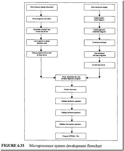
Monitors , Flowcharts , Basic Features of Microcomputer Development Systems , System Development Flowchart , QUESTIONS AND PROBLEMS

6.7 Monitors

A monitor consists of a number of subroutines grouped together to provide "intelligence" to a microcomputer system. This intelligence gives the microcomputer with the capabilities for software development of user programs such as assembling and debugging. The monitor is typically offered by the microprocessor manufacturers and others in a ROM or CD memory. When a microcomputer is designed by connecting the microprocessor, memory, and I/O, a monitor program can be used for development of user programs.

An example of a monitor is the Intel SDK-86 monitor, which contains debugging

routines, a display routine, and many other programs. The user can assemble, debug, execute and display results for user-written 8086 assembly language programs using the monitor provided by Intel with the SDK-86 microcomputer.

6.8 Flowcharts

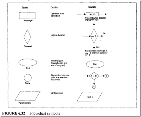
Before writing an assembly language program for a specific operation, it is convenient to represent the program in a schematic form called flowchart. A brief listing of the basic shapes used in a flowchart and their functions is given in Figure 6.32.

6.9 Basic Features of Microcomputer Development Systems

A microcomputer development system is a tool that allows the designer to develop, debug, and integrate error-free application software in microprocessor systems.

Development systems fall into one of two categories: systems supplied by the device manufacturer (nonuniversal systems) and systems built by after-market manufacturers (universal systems). The main difference between the two categories is the range of microprocessors that a system will accommodate. Nonuniversal systems are supplied by the microprocessor manufacturer (Intel, Motorola) and are limited to use for the particular microprocessor manufactured by the supplier. In this manner, an Intel development system may not be used to develop a Motorola-based system. The universal development systems (Hewlett-Packard, Tektronix) can develop hardware and software for several microprocessors.

image

Within both categories of development systems, there are basically three types available: single-user systems, time-shared systems, and networked systems. A single-user system consists of one development station that can be used by one user at a time. Single­ user systems are low in cost and may be sufficient for small systems development. Time­ shared systems usually consist of a "dumb" type of terminal connected by data lines to a centralized microcomputer-based system that controls all operations. A networked system usually consists of a number of smart cathode ray tubes (CRTs) capable of performing most of the development work and can be connected over data lines to a central microcomputer. The central microcomputer in a network system usually is in charge of allocating disk storage space and will D0wnload some programs into the user’s workstation microcomputer. A microcomputer development system is a combination of the hardware necessary for microprocessor design and the software to control the hardware. The basic components of the hardware are the central processor, the CRT terminal, mass storage device (floppy or hard disk), and usually an in-circuit emulator (ICE).

In a single-user system, the central processor executes the operating system software, handles the input/output (I/O) facilities, executes the development programs (editor, assembler, linker), and allocates storage space for the programs in execution. In a large multiuser networked system the central processor may be responsible for the I/O facilities and execution of development programs. The CRT terminal provides the interface between the user and the operating system or program under execution. The user enters commands or data via the CRT keyboard, and the program under execution displays data to the user via the CRT screen. Each program (whether system software or user program) is stored in an ordered format on disk. Each separate entry on the disk is called afile. The operating system software contains the routines necessary to interface between the user and the mass storage unit. When the user requests a file by a specific file name, the operating system finds the program stored on disk by the file name and loads it into mean memory. More advanced development systems contain memory management software that protects a user’s files from unauthorized modification by another user. This is accomplished via a unique- user identification code called USER ID. A user can only access files that have the user’s unique code. The equipment listed here makes up a basic development system, but most systems have other devices such as printers and EPROM and PAL programmers attached. A printer is needed to provide the user with a hard copy record of the program under development.

After the application system software has been completely developed and debugged, it needs to be permanently stored for execution in the target hardware. The EPROM (erasable/programmable read-only memory) programmer takes the machine code and programs it into an EPROM. EPROMs are more generally used in system development because they may be erased and reprogrammed if the program changes. EPROM programmers usually interface to circuits particularly designed to program a specific EPROM.

Most development systems support one or more in-circuit emulators (ICEs).

The ICE is one of the most advanced tools for microprocessor hardware development. To use an ICE, the microprocessor chip is removed from the system under development (called the target processor) and the emulator is plugged into the microprocessor socket. The ICE will functionally and electrically act identically to the target processor with the exception that the ICE is under the control of development system software. In this manner the development system may exercise the hardware that is being designed and monitor all status information available about the operation of the target processor. Using an ICE, processor register contents may be displayed on the CRT and operation of the hardware observed in a single-stepping mode. In-circuit emulators can find hardware and software bugs quickly that might take many hours to locate using conventional hardware testing methods.

Architectures for development systems can be generally divided into two categories: the master/slave configuration and the single-processor configuration. In a master/slave configuration, the master (host) processor controls the mass storage device and processes all I/O (CRT, printer). The software for development systems is written for the master processor, which is usually not the same as the slave (target) processor. The slave microprocessor is typically connected to the user prototype via a connector which links the slave processor to the master processor.

Some development systems such as the HP 64000 completely separate the system bus from the emulation bus and therefore use a separate block of memory for emulation. This separation allows passive monitoring of the software executing on the target processor without stopping the emulation process. A benefit of the separate emulation facilities allows the master processor to be used for editing, assembling, and so on while the slave processor continues the emulation. A designer may therefore start an emulation running, exit the emulator program, and at some future time return to the emulation program.

Another advantage of the separate bus architecture is that an operating system needs to be written only once for the master processor and will be used no matter what type of slave processor is being emulated. When a new slave processor is to be emulated, only the emulator probe needs to be changed.

A disadvantage of the master/slave architecture is that it is expensive. In single­ processor architecture, only one processor is used for system operation and target emulation. The single processor D0es both jobs, executing system software as well as acting as the target processor. Because there is only one processor involved, the system software must be rewritten for each type of processor that is to be emulated. Because the system software must reside in the same memory used by the emulator, not all memory will be available to the emulation process, which may be a disadvantage when large prototypes are being developed. The single-processor systems are inexpensive.

The programs provided for microprocessor development are the operating system, editor, assembler, linker, compiler, and debugger. The operating system is responsible for executing the user’s commands. The operating system handles I/O functions, memory management, and loading of programs from mass storage into RAM for execution. The editor allows the user to enter the source code (either assembly language or some high­ levellanguage) into the development system.

Almost all current microprocessor development systems use the character­ oriented editor, more commonly referred to as the screen editor. The editor· is called a "screen editor" because the text is dynamically displayed on the screen and the display automatically updates any edits made by the user.

The screen editor uses the pointer concept to point to the character(s) that need editing. The pointer in a screen editor is called the "cursor," and special commands allow the user to position the cursor to any location displayed on the screen. When the cursor is positioned, the user may insert characters, delete characters, or simply type over the existing characters.

Complete lines may be added or deleted using special editor commands. By placing the editor in the insert mode, any text typed will be inserted at the cursor position when the cursor is positioned between two existing lines. If the cursor is positioned on a line to be deleted, a single command will remove the entire line from the file.

Screen editors implement the editor commands in different fashions. Some editors use dedicated keys to provide some cursor movements. The cursor keys are usually marked with arrows to show the direction of the cursor movement. More advanced editors (such as the HP 64000) use soft keys. A soft key is an unmarked key located on the keyboard directly below the bottom of the CRT screen. The mode of the editor decides what functions the keys are to perform. The function of each key is displayed on the screen directly above the appropriate key. The soft key approach is valuable because it allows the editor to reassign a key to a new function when necessary.

The source code generated on the editor is stored as ASCII or text characters and cannot be executed by a microprocessor. Before the code can be executed, it must be converted to a form accessible by the microprocessor. An assembler is the program used to translate the assembly language source code generated with an editor into object code (machine code), which may be executed by a microprocessor.

The output file from most development system assemblers is an object file. The object file is usually relocatable code that may be configured to execute at any address. The function of the linker is to convert the object file to an absolute file, which consists of the actual machine code at the correct address for execution. The absolute files thus created are used for debugging and finally for programming EPROMs.

Debugging a microprocessor-based system may be divided into two categories:

software debugging and hardware debugging. Both debugging processes are usually carried out separately because software debugging can be carried out on an out-of-circuit emulator (OCE) without having the final system hardware.

The usual software development tools provided with the development system are Single-step facility Breakpoint facility

A single stepper simply allows the user to execute the program being debugged one instruction at a time. By examining the register and memory contents during each step, the debugger can detect such program faults as incorrect jumps, incorrect addressing, erroneous op-codes, and so on. A breakpoint allows the user to execute an entire section of a program being debugged.

There are two types of breakpoints: hardware and software. The hardware breakpoint uses the hardware to monitor the system address bus and detect when the program is executing the desired breakpoint location. When the breakpoint is detected, the hardware uses the processor control lines to halt the processor for inspection or cause the processor to execute an interrupt to a breakpoint routine. Hardware breakpoints can be used to debug both ROM- and RAM-based programs. Software breakpoint routines may only operate on a system with the program in RAM because the breakpoint instruction must be inserted into the program that is to be executed.

Single-stepper and breakpoint methods complement each other. The user may insert a breakpoint at the desired point and let the program execute up to that point. When the program stops at the breakpoint the user may use a single-stepper to examine the program one instruction at a time. Thus, the user can pinpoint the error in a program.

There are two main hardware-debugging tools: the logic analyzer and the in-circuit emulator. Logic analyzers are usually used to debug hardware faults in a system. The logic analyzer is the digital version of an oscilloscope because it allows the user to view logic levels in the hardware. In-circuit emulators can be used to debug and integrate software and hardware. PC-based workstations are extensively used as development systems.

6.10 System Development Flowchart

The total development of a microprocessor-based system typically involves three phases: software design, hardware design, and program diagnostic design. A systems programmer will be assigned the task of writing the application software, a logic designer will be assigned the task of designing the hardware, and typically both designers will be assigned the task of developing diagnostics to test the system. For small systems, one engineer may D0 all three phases, while on large systems several engineers may be assigned to each phase. Figure 6.33 shows a flowchart for the total development of a system. Notice that software and hardware development may occur in parallel to save time.

The first step in developing the software is to take the system specifications and

write a flowchart to accomplish the desired tasks that will implement the specifications. The assembly language or high-level source code may now be written from the system flowchart. The complete source code is then assembled. The assembler is the object code and a program listing. The object code will be used later by the linker. The program listing may be sent to a disk file for use in debugging, or it may be directed to the printer.

The linker can now take the object code generated by the assembler and create

image

the final absolute code that will be executed on the target system. The emulation phase will take the absolute code and load it into the development system RAM. From here, the program may be debugged using breakpoints or single stepping.

Working from the system specifications, a block diagram of the hardware must

be developed. The logic diagram and schematics may now be drawn using the block diagram as a guide, and a prototype may now be constructed and tested for wiring errors. When the prototype has been constructed it may be debugged for correct operation using standard electronic testing equipment such as oscilloscopes, meters, logic probes, and logic analyzers, all with test programs created for this purpose. After the prototype has been debugged electrically, the development system in-circuit emulator may be used to check it functionally. The ICE will verify the memory map, correct 110 operation, and so on. The next step in system development is to validate the complete system by running operational checks on the prototype with the finalized application software installed. The EPROMs and/or PALs are then programmed with the error-free programs.

QUESTIONS AND PROBLEMS

6.1 What is the difference between a single-chip microprocessor and a single-chip microcomputer?

6.2 What is a microcontroller? Name one commercially available microcontroller.

6.3 What is the difference between:

(a) The program counter (PC) and the memory address register (MAR)?

(b) The accumulator (A) and the instruction register (IR)?

(c) General-purpose register-based microprocessor and accumulator-based microprocessor. Name a commercially available microprocessor of each type.

6.4 Assuming signed numbers, find the sign, carry, zero, and overflow flags of: (a) 0916 + 1716.

(b) A5 16 – A516

(c) 71 16 -A916

(d) 6E16 + 3AI6

(e) 7E 16 + 7EI6

6.5 What is meant by PUSH and POP operations in the stack?

6.6 Suppose that an 8-bit microprocessor has a 16-bit stack pointer and uses a 16-bit register to access the stack from the top. Assume that initially the stack pointer and the 16-bit register contain 20C0 16 and 0205 16 respectively. After the PUSH operation:

(a) What are the contents of the stack pointer?

(b) What arc the contents of memory locations 20BE 16 and 20BF16?

6.7 Assuming the microprocessor architecture of Figure 6.18, write D0wn a possible sequence of microinstructions for finding the ones complement of an 8-bit number. Assume that the number is already in the register.

6.8 What D0 you mean by a multiplexed address and data bus?

6.9 Name four general-purpose registers in the 8086.

6.10 Name one 8086 register that can be used to hold an address in a segment.

6.11 What is the difference between EPROM and PROM? Are both types available with bipolar and also MOS technologies?

6.12 Assuming a single clock signal and four registers (PC, MAR, Reg, and IR) for a microprocessor, draw a timing diagram for loading the memory address register. Explain the sequence of events relating them to the four registers.

6.13 Given a memory with a 14-bit address and 8-bit word size.

(a) How many bytes can be stored in this memory?

(b) If this memory were constructed from 1K x 1-bit RAMs, how many memory chips would be required?

(c) How many bits would be used for chip select?

6.14 Define the three types of I/O. Identify each one as either "microprocessor initiated" or "device initiated."

6.15 What is the basic difference between a compiler and an assembler?

6.16 Write a program equivalent to the Pascal assignment statement:

Z := (A + (B * C) + (D * E) – (F / G) – (H * I)

Use only

(a) Three-address instructions

(b) Two-address instructions

6.17 Describe the meaning of each one of the following addressing modes.

image

6.18 Assume that a microprocessor has only two registers R1 and R2 and that only the following instruction is available:

image


Using this XOR instruction, find an instruction sequence in order to exchange the contents of registers Rl and R2

6.19 What are the advantages of subroutines?

6.20 Explain the use of a stack in implementing subroutine calls.

6.21 Determine the contents of address 5004 16 after assembling the following:

image6.22 What is the difference between:

(a) A cross assembler and a resident assembler

(b) A two-pass assembler and meta-assembler

(c) Single step and breakpoint

6.23 Identify some of the differences between C, C++, and Java.

6.24 How D0es a microprocessor obtain the address of the first instruction to be executed?

6.25 Summarize the basic features of a typical microcomputer development system.

6.26 Discuss the steps involved in designing a microprocessor-based system.


Microcomputer Programming Concepts: Microcomputer Programming Languages , Machine Language , Assembly Language and High-Level Languages

6.6 Microcomputer Programming Concepts

This section includes the fundamental concepts of microcomputer programming. Typical programming characteristics such as programming languages, microprocessor instruction sets, addressing modes, and instruction formats are discussed.

6.6.1 Microcomputer Programming Languages

Microcomputers are typically programmed using semi-English-language statements (assembly language). In addition to assembly languages, microcomputers use a more understandable human-oriented language called the "high-level language." No matter what type oflanguage is used to write the programs, the microcomputers only understand binary numbers. Therefore, the programs must eventually be translated into their appropriate binary forms. The main ways of accomplishing this are discussed later.

Microcomputer programming languages can typically be divided into three main types:

1. Machine language

2. Assembly language

3. High-levellanguage

A machine language program consists of either binary or hexadecimal op-codes. Programming a microcomputer with either one is relatively difficult, because one must deal only with numbers. The architecture and microprograms of a microprocessor determine

image

ll its instructions. These instructions are called the microprocessor’s "instruction set." Programs in assembly and high-level languages are represented by instructions that use English- language-type statements. The programmer finds it relatively more convenient to write the programs in assembly or a high-level language than in machine language. However, a translator must be used to convert the assembly or high-level programs into binary machine language so that the microprocessor can execute the programs. This is shown in Figure 6.30.

An assembler translates a program written in assembly language into a machine

language program. A compiler or interpreter, on the other hand, converts a high-level language program such as C or C++ into a machine language program. Assembly or high­ level language programs are called "source codes." Machine language programs are known as "object codes." A translator converts source codes to object codes. Next, we discuss the three main types of programming language in more detail.

6.6.2 Machine Language

A microprocessor has a unique set of machine language instructions defined by its manufacturer. No two microprocessors by two different manufacturers have the same machine language instruction set. For example, the Intel 8086 microprocessor uses the code OlD8 16 for its addition instruction whereas the Motorola 68000 uses the code D282 16• Therefore, a machine language program for one microcomputer will not usually run on another microcomputer of a different manufacturer.

At the most elementary level, a microprocessor program can be written using its instruction set in binary machine language. As an example, a program written for adding two numbers using the Intel 8086 machine language is

imageObviously, the program is very difficult to understand, unless the programmer remembers all the 8086 codes, which is impractical. Because one finds it very inconvenient to work with I’sand O’s, it is almost impossible to write an error-free program at the first try. Also, it is very tiring for the programmer to enter a machine language program written in binary into the microcomputer’s RAM. For example, the programmer needs a number of binary switches to enter the binary program. This is definitely subject to errors.

To increase the programmer’s efficiency in writing a machine language program,

hexadecimal numbers rather than binary numbers are used. The following is the same addition program in hexadecimal, using the Intel 8086 instruction set:

imageIt is easier to detect an error in a hexadecimal program, because each byte contains only two hexadecimal digits. One would enter a hexadecimal program using a hexadecimal

keyboard. A keyboard monitor program in ROM, usually offered by the manufacturer, provides interfacing of the hexadecimal keyboard to the microcomputer. This program converts each key actuation into binary machine language in order for the microprocessor to understand the program. However, programming in hexadecimal is not normally used.

6.6.3 Assembly Language

The next programming level is to use the assembly language. Each line in an assembly language program includes four fields:

I. Label field

2. Instruction, mnemonic, or op-code field

3. Operand field

4. Comment field

As an example, a typical program for adding two 16-bit numbers written in 8086 assembly language is

image

Obviously, programming in assembly language is more convenient than programming in machine language, because each mnemonic gives an idea of the type of operation it is supposed to perform. Therefore, with assembly language, the programmer Does not have to find the numerical op-codes from a table of the instruction set, and programming efficiency is significantly improved.

The assembly language program is translated into binary via a program called

an "assembler." The assembler program reads each assembly instruction of a program as ASCII characters and translates them into the respective binary op-codes. As an example, consider the HLT instruction for the 8086. Its binary op-code is 1111 0100. An assembler would convert HLT into 111 0100 as shown in Figure 6.31.

An advantage of the assembler is address computation. Most programs use addresses

within the program as data storage or as targets for jumps or calls. When programming in machine language, these addresses must be calculated by hand. The assembler solves this problem by allowing the programmer to assign a symbol to an address. The programmer may then reference that address elsewhere by using the symbol. The assembler computes the actual address for the programmer and fills it in automatically. One can obtain hands-

image

on experience with a typical assembler for a microprocessor by D0wnloading it from the Internet.

Most assemblers use two passes to assemble a program. This means that they read the input program text twice. The first pass is used to compute the addresses of all labels in the program. In order to find the address of a label, it is necessary to know the total length of all the binary code preceding that label. Unfortunately, however, that address may be needed in that preceding code. Therefore, the first pass computes the addresses of all labels and stores them for the next pass, which generates the actual binary code. Various types of assemblers are available today. We define some of them in the following paragraphs.

  •  One-Pass Assembler. This assembler goes through the assembly language program once and translates it into a machine language program. This assembler has the problem of defining forward references. This means that a JUMP instruction using an address that appears later in the program must be defined by the programmer after the program is assembled.
  • Two-Pass Assembler. This assembler scans the assembly language program twice. In the first pass, this assembler creates a symbol table. A symbol table consists of labels with addresses assigned to them. This way labels can be used for JUMP statements and no address calculation has to be D0ne by the user. On the second pass, the assembler translates the assembly language program into the machine code. The two-pass assembler is more desirable and much easier to use.
  • Macroassembler. This type of assembler translates a program written in macrolanguage into the machine language. This assembler lets the programmer define all instruction sequences using macros. Note that, by using macros, the programmer can assign a name to an instruction sequence that appears repeatedly in a program. The programmer can thus avoid writing an instruction sequence that is required many times in a program by using macros. The macroassembler replaces a macroname with the appropriate instruction sequence each time it encounters a macroname.

It is interesting to see the difference between a subroutine and a macroprogram. A specific subroutine occurs once in a program. A subroutine is executed by CALLing it from a main program. The program execution jumps out of the main program and then executes the subroutine. At the end of the subroutine, a RET instruction is used to resume program execution following the CALL SUBROUTINE instruction in the main program. A macro, on the other hand, D0es not cause the program execution to branch out of the main program. Each time a macro occurs, it is replaced with the appropriate instruction sequence in the main program. Typical advantages of using macros are shorter source programs and better program D0cumentation. A disadvantage is that effects on registers and flags may not be obvious.

Conditional macroassembly is very useful in determining whether or not an

instruction sequence is to be included in the assembly depending on a condition that is true or false. If two different programs are to be executed repeatedly based on a condition that can be either true or false, it is convenient to use conditional macros. Based on each condition, a particular program is assembled. Each condition and the appropriate program are typically included within IF and ENDIF pseuD0-instructions.

  •  Cr-oss Assembler. This type of assembler is typically resident in a processor and

assembles programs for another for which it is written. The cross assembler program is written in a high-level language so that it can run on different types of processors that understand the same high-level language.

  •  Resident Assembler. This type of assembler assembles programs for a processor

in which it is resident. The resident assembler may slow D0wn the operation of the processor on which it runs.

  •  Meta-assembler. This type of assembler can assemble programs for many different  types of processors. The programmer usually defines the particular processor being used.

As mentioned before, each line of an assembly language program consists of four fields: label, mnemonic or op-code, operand, and comment. The assembler ignores the comment field but translates the other fields. The label field must start with an uppercase alphabetic character. The assembler must know where one field starts and another ends. Most assemblers allow the programmer to use a special symbol or delimiter to indicate the beginning or end of each field. Typical delimiters used are spaces, commas, semicolons, and colons:

  • Spaces are used between fields.
  • Commas (,) are used between addresses in an operand field.
  • A semicolon (;) is used before a comment.
  • A colon (:) or no delimiter is used after a label.

To handle numbers, most assemblers consider all numbers as decimal numbers unless specified. Most assemblers will also allow binary, octal, or hexadecimal numbers. The user must define the type of number system used in some way. 1his is usually D0ne by using a letter following the number. Typical letters used are

  • B for binary
  • Q for octal
  • H for hexadecimal

Assemblers generally require hexadecimal numbers to start with a digit. A 0 is typically used if the first digit of the hexadecimal number is a letter. This is D0ne to distinguish between numbers and labels. For example, most assemblers will require the number ASH to be represented as OA5H.

Assemblers use pseuD0-instructions or directives to make the formatting of the edited text easier. These pseuD0-instructions are not directly translated into machine language instructions. They equate labels to addresses, assign the program to certain areas of memory, or insert titles, page numbers, and so on. To use the assembler directives or pseuD0-instructions, the programmer puts them in the op-code field, and, if the pseuD0­ instructions require an address or data, the programmer places them in the label or data field. Typical pseuD0-instructions are ORIGIN (ORG), EQUATE (EQU), DEFINE BYTE (DB), and DEFINE WORD (DW).

ORIGIN (ORG)

The pseuD0-instruction ORG lets the programmer place the programs anywhere in memory. Internally, the assembler maintains a program-counter-type register called the "address counter." This counter maintains the address of the next instruction or data to be processed.

An ORG pseuD0-instruction is similar in concept to the JUMP instruction. Recall that the JUMP instruction causes the processor to place a new address in the program counter. Similarly, the ORG pseuD0-instruction causes the assembler to place a new value in the address counter.

Typical ORG statements are

ORG 7000H

CLC

The 8086 assembler will generate the following code for these statements:

7000 F8

Most assemblers assign a value of zero to the starting address of a program if the programmer D0es not define this by means of an ORG.

Equate (EQU)

The pseuD0-instruction EQU assigns a value in its operand field to an address in its label field. This allows the user to assign a numeric value to a symbolic name. The user can then use the symbolic name in the program instead of its numeric value. This reduces errors.

A typical example ofEQU is START EQU 0200H, which assigns the value 0200 in hexadecimal to the label START. Another example is

image

In this example, the EQU gives PORTA the value 40 hex, and FF hex is the data to be written into register AL by MOV AL, OFFH. OUT PORTA, AL then outputs this data FF hex to port 40, which has already been equated to PORTA before.

Note that, if a label in the operand field is equated to another label in the label field, then the label in the operand field must be previously defined. For example, the EQU statement

BEGIN               EQU               START

will generate an error unless START is defined previously with a numeric value.

Define Byte (DB)

The pseuD0-instruction DB is usually used to set a memory location to certain byte value. For example,

START             DB                45H

will store the data value 45 hex to the address START.

With some assemblers, the DB pseuD0-instruction can be used to generate a table of data as follows:

image

In this case, 20 hex is the first data of the memory location 7000; 30 hex, 40 hex, and 50 hex occupy the next three memory locations. Therefore, the data in memory will look like this:

image

Note that some assemblers use DC.B instead of DB. DC stands for Define Constant.

Define Word (DW)

The pseuD0-instruction DW is typically used to assign a 16-bit value to two memory locations. For example,

imagewill assign C2 to location 7000 and 4A to location 700 I. It is assumed that the assembler will assign the low byte first (C2) and then the high byte (4A).

With some assemblers, the DW pseuD0-instruction can be used to generate a table of 16-bit data as follows:

image

In this case, the three 16-bit values 5000H, 6000H, and 7000H are assigned to memory locations starting at the address 8000H. That is, the array would look like this:

image

Note that some assemblers use DC.W instead ofDW.

Assemblers also use a number of housekeeping pseuD0-instructions. Typical housekeeping pseuD0-instructions are TITLE, PAGE, END, and LIST. The following are the housekeeping pseuD0-instructions that control the assembler operation and its program listing.

TITLE prints the specified heading at the top of each page of the program listing. For example,

TITLE "Square Root Algorithm"

will print the name "Square Root Algorithm" on top of each page.

PAGE skips to the next line.

END indicates the end of the assembly language source program.

LIST directs the assembler to print the assembler source program.

In the following, assembly language instruction formats, instruction sets, and addressing modes available with typical microprocessors will be discussed.

Assembly Language Instruction Formats

Depending on the number of addresses specified, we have the following instruction

formats:

  • Three address
  • Two address
  • One address
  • Zero address

Because all instructions are stored in the main memory, instruction formats are designed in such a way that instructions take less space and have more processing capabilities. It should be emphasized that the microprocessor architecture has considerable influence on a specific instruction format. The following are some important technical points that have to be considered while designing an instruction format:

  • The size of an instruction word is chosen in such a way that it facilitates the specification of more operations by a designer. For example, with 4- and 8-bit op-code fields, we can specify 16 and 256 distinct operations respectively.
  • Instructions are used to manipulate various data elements such as integers, floating­ point numbers, and character strings. In particular, all programs written in a symbolic language such as C are internally stored as characters. Therefore, memory space will not be wasted if the word length of the machine is some integral multiple of the number of bits needed to represent a character. Because all characters are represented using typical 8-bit character codes such as ASCII or EBCDIC, it is desirable to have 8-, I 6-, 32-, or 64-bit words for the word length.
  • The size of the address field is chosen in such a way that a high resolution is guaranteed. Note that in any microprocessor, the ultimate resolution is a bit. Memory resolution is function of the instruction length, and in particular, short instructions provide less resolution. For example, in a microcomputer with 32K 16-bit memory words, at least 19 bits are required to access each bit of the word. (This is because 2 15 = 32K and 24 = 16)

The general form of a three address instruction is shown below:

<op-code> Addrl, Addr2, Addr3

Some typical three-address instructions are

image

In this specification, all alphabetic characters are assumed to represent memory addresses, and the string that begins with the letter R indicates a register. The third address of this type of instruction is usually referred to as the "destination address." The result of an operation is always assumed to be saved in the destination address.

Typical programs can be written using these. three address instructions. For example, consider the following sequence of three address instructions

imageThis sequence implements the statement z = A * B + C * D – E * F. The three-address format is normally used by 32-bit microprocessors in addition to the other formats.

If we drop the third address from the three-address format, we obtain the two­ address format. Its general form is

<op-code> Addrl, Addr2

Some typical two-address instructions are

image

In this format, the addresses Addrl and Addr2 respectively represent source and destination addresses. The following sequence of two-address instructions is equivalent to the program using three-address format presented earlier:

imageThis format is preD0minant in typical general-purpose microprocessors such as the Intel 8086 and the Motorola 68000. Typical 8-bit microprocessors such as the Intel 8085 and the Motorola 6809 are accumulator based. In these microprocessors, the accumulator register is assumed to be the destination for all arithmetic and logic operations. Also, this register always holds one of the source operands. Thus, we only need to specify one address in the instruction, and therefore, this idea reduces the instruction length. The one-address format is preD0minant in 8-bit microprocessors. Some typical one-address instructions are

image

In this program, Tl and T2 represent the addresses of memory locations used to store temporary results. Instructions that D0 not require any addresses are called "zero­ address instructions." All microprocessors include some zero-address instructions in the instruction set. Typical examples of zero-address instructions are CLC (clear carry) and NOP.

Typical Assembly Language Instruction Sets

An instruction set of a specific microprocessor consists of all the instructions that it can execute. The capabilities of a microprocessor are determined, to some extent, by the types of instructions it is able to perform. Each microprocessor has a unique instruction set designed by its manufacturer to D0 a specific task. We discuss some of the instructions that are common to all microprocessors. We will group chunks of these instructions together which have similar functions. These instructions typically include

Data Processing Instructions. These operations perform actual data manipulations.

The instructions typically include arithmetic/logic operations and increment/ decrement and rotate/shift operations. Typical arithmetic instructions include ADD, SUBTRACT, COMPARE, MULTIPLY, AND DIVIDE. Note that the SUBTRACT

instruction provides the result and also affects the status flags while the COMPARE instruction performs subtraction without any result and affects the flags based on the result. Typical logic instructions perform traditional Boolean operations such as AND, OR, and EXCLUSIVE-OR. The AND instruction can be used to perform a masking operation. If the bit value in a particular bit position is desired in a word, the

word can be logically ANDed with appropriate data to accomplish this. For example, the bit value at bit 2 of an 8-bit number 0100 1Y 10 (where unknown bit value of Y is to be determined) can be obtained as follows:

image

If the bit value Y at bit 2 is 1, then the result is nonzero (Flag Z=O); otherwise, the result is zero (Flag Z= 1) . The Z flag can be tested using typical conditional JUMP instructions such as JZ (Jump if Z= 1) or JNZ(Jump if Z=O) to determine whether Y is 0 or 1. This is called masking operation. The AND instruction can also be used to determine whether a binary number is ODD or EVEN by checking the Least Significant bit (LSB) of the number (LSB=O for even and LSB= 1 for odd). The OR instruction can typically be used to insert a 1 in a particular bit position of a binary number without changing the values of the other bits. For example, a 1 can be inserted using the OR instruction at bit number 3 of the 8-bit binary number 0 1 1 1 0 0 1 1 without changing the values of the other bits as follows:


image

  • Instructions for Controlling Microprocessor Operations. These instructions typically include those that set the reset specific flags and halt or stop the microprocessor.
  • Data Movement Instructions. These instructions move data from a register to memory and vice versa, between registers, and between a register and an I/O device.
  • Instructions Using Memory Addresses. An instruction in this category typically contains a memory address, which is used to read a data word from memory into a microprocessor register or for writing data from a register into a memory location. Many instructions under data processing and movement fall in this category.
  • Conditional and Unconditional JUMPS. These instructions typically include one of the following:

1. Unconditional JUMP, which always transfers the memory address specified in the instruction into the program counter.

2. Conditional JUMP, which transfers the address portion of the instruction into the

program counter based on the conditions set by one of the status flags in the flag register.

Typical Assembly Language Addressing Modes

One of the tasks performed by a microprocessor during execution of an instruction is the determination of the operand and destination addresses. The manner in which a microprocessor accomplishes this task is called the "addressing mode." Now, let us present the typical microprocessor addressing modes, relating them to the instruction sets of Motorola 68000.

An instruction is said to have "implied or inherent addressing mode" if it D0es not have any operand. For example, consider the following instruction: RTS, which means "return from a subroutine to the main program." The RTS instruction is a no-operand instruction. The program counter is implied in the instruction because although the program counter is not included in the RTS instruction, the return address is loaded in the program counter after its execution.

Whenever an instruction/operand contains data, it is called an "immediate mode"

instruction. For example, consider the following 68000 instruction:

ADD #15, D0 D0 <- D0 + 15

In this instruction, the symbol # indicates to the assembler that it is an immediate mode

instruction. This instruction adds 15 to the contents of register D0 and then stores the result in D0. An instruction is said to have a register mode if it contains a register as opposed to a memory address. This means that the operand values are held in the microprocessor registers. For example, consider the following 68000 instruction:

ADD D1, D0 ; D0 <- D1 + D0

This ADD instruction is a two-operand instruction. Both operands (source and destination) have register mode. The instruction adds the 16-bit contents of D0 to the 16-bit contents ofD1 and stores the 16-bit result in D0.

An instruction is said to have an absolute or direct addressing mode if it contains a memory address in the operand field. For example, consider the 68000 instruction

ADD 3000, D2

This instruction adds the 16-bit contents of memory address 3000 to the 16- bit contents of D2 and stores the 16-bit result in D2. The source operand to this ADD instruction contains 3000 and is in absolute or direct addressing mode. When an instruction specifies a microprocessor register to hold the address, the resulting addressing mode is known as the "register indirect mode." For example, consider the 68000 instruction:

CLR (AO)

This instruction clears the 16-bit contents of a memory location whose address is in register AO to zero. The instruction is in register indirect mode.

The conditional branch instructions are used to change the order of execution of a program based on the conditions set by the status flags. Some microprocessors use conditional branching using the absolute mode. The op-code verifies a condition set by a particular status flag. If the condition is satisfied, the program counter is changed to the value ofthe operand address (defined in the instruction). If the condition is not satisfied, the program counter is incremented, and the program is executed in its normal order.

Typical 16-bit microprocessors use conditional branch instructions. Some conditional branch instructions are 16 bits wide. The first byte is the op-code for checking a particular flag. The second byte is an 8-bit offset, which is added to the contents of the program eounter if the condition is satisfied to determine the effective address. This offset is considered as a signed binary number with the most significant bit as the sign bit. It means that the offset can vary from -12810 to +127 10 (0 being positive). This is called relative mode.

Consider the following 68000 example, which uses the branch not equal (BNE) instruction:

BNE 8

Suppose that the program counter contains 2000 (address of the next instruction to be executed) while executing this BNE instruction. Now, if Z = 0, the microprocessor will load 2000 + 8 = 2008 into the program counter and program execution resumes at address 2008. On the other hand, if Z = 1, the microprocessor continues with the next instruction.

In the last example the program jumped forward, requiring positive offset. An example for branching with negative offset is

BNE -14

image

Therefore, to branch backward to 1FF6 16, the assembler uses an offset of F2 following the op-code for BNE.

An advantage of relative mode is that the destination address is specified relaive to the address of the instruction after the instruction. Since these conditional Jump instructions D0 not contain an absolute address, the program can be placed anywhere in memory which can still be excuted properly by the microprocessor. A program which can be placed anywhere in memory, and can still run correctly is called a "relocatable" program. It is a good practice to write relocatable programs.

Subroutine Calls in Assembly Language

It is sometimes desirable to execute a common task many times in a program. Consider the case when the sum of squares of numbers is required several times in a program. One could write a sequence of instructions in the main program for carrying out the sum of squares every time it is required. This is all right for short programs. For long programs, however, it is convenient for the programmer to write a small program known as a "subroutine" for performing the sum of squares, and then call this program each time it is needed in the main program.

Therefore, a subroutine can be defined as a program carrying out a particular function that can be called by another program known as the "main program." The subroutine only needs to be placed once in memory starting at a particular memory location. Each time the main program requires this subroutine, it can branch to it, typically by using a jump to subroutine (JSR) instruction along with its starting address. The subroutine is then executed. At the end of the subroutine, a RETURN instruction takes control back to the main program.

The 68000 includes two subroutine call instructions. Typical examples include JSR 4 00 0 and BSR 2 4. JSR 4 0 0 0 is an instruction using absolute mode. In response to the execution of JSR, the 68000 saves (pushes) the current program counter contents (address of the next instruction to be executed) onto the stack. The program counter is then

loaded, with 4000 included in the JSR instruction. The starting address of the subroutine is 4000. The RTS (return from subroutine) at the end of the subroutine reads (pops) the return address saved into the stack before jumping to the subroutine into the program counter. The program execution thus resumes in the main program. BSR 2 4 is an instruction using relative mode. This instruction works in the same way as the JSR 4 0 0 0 except that displacement 2 4 is added to the current program counter contents to jump to the subroutine.

The stack must always be balanced. This means that a PUSH instruction in a

subroutine must be followed by a POP instruction before the RETURN from subroutine instruction so that the stack pointer points to the right return address saved onto the stack. This will ensure returning to the desired location in the main program after execution of the subroutine. If multiple registers are PUSHED in a subroutine, one must POP them in the reverse order before the subroutine RETURN instruction.

6.6.4 High-Level Languages

As mentioned before, the programmer’s efficiency with assembly language increases significantly compared to machine language. However, the programmer needs to be well acquainted with the microprocessor’s architecture and its instruction set. Further, the programmer has to provide an op-code for each operation that the microprocessor has to carry out in order to execute a program. As an example, for adding two numbers, the programmer would instruct the microprocessor to load the first number into a register, add the second number to the register, and then store the result in memory. However, the programmer might find it tedious to write all the steps required for a large program. Also, to become a reasonably good assembly language programmer, one needs to have a lot of experience.

High-level language programs composed of English-language-type statements rectify all these deficiencies of machine and assembly language programming. The programmer D0es not need to be familiar with the internal microprocessor structure or its instruction set. Also, each statement in a high-level language corresponds to a number of assembly or machine language instructions. For example, consider the statement F = A + B written in a high-level language called FORTRAN. This single statement adds the contents of A with B and stores the result in F. This is equivalent to a number of steps in machine or assembly language, as mentioned before. It should be pointed out that the letters A, B, and F D0 not refer to particular registers within the microprocessor. Rather, they are memory locations.

A number of high-level languages such as C and C++ are widely used these days. Typical microprocessors, namely, the Intel 8086, the Motorola 68000, and others, can be programmed using these high-level languages. A high-level language is a problem­ oriented language. The programmer D0es not have to know the details of the architecture of the microprocessor and its instruction set. Basically, the programmer follows the rules of the particular language being used to solve the problem at hand. A second advantage is that a program written in a particular high-level language can be executed by two different microcomputers, provided they both understand that language. For example, a program written in C for an Intel 8086-based microcomputer will run on a Motorola 68000-based microcomputer because both microprocessors have a compiler to translate the C language into their particular machine language; minor modifications are required for input/output programs.

As mentioned before, like the assembly language program, a high-level language program requires a special program for converting the high-level statements into object codes. This program can be either an interpreter or a compiler. They are usually very large programs compared to assemblers.

An interpreter reads each high-level statement such as F = A + Band directs the microprocessor to perform the operations required to execute the statement. The interpreter converts each statement into machine language codes but D0es not convert the entire program into machine language codes prior to execution. Hence, it D0es not generate an object program. Therefore, an interpreter is a program that executes a set of machine language instructions in response to each high-level statement in order to carry out the function. A compiler, however, converts each statement into a set of machine language instructions and also produces an object program that is stored in memory. This program must then be executed by the microprocessor to perform the required task in the high­ level program. In summary, an interpreter executes each statement as it proceeds, without generating an object code, whereas a compiler converts a high-level program into an object program that is stored in memory. This program is then executed. Compilers normally provide inefficient machine codes because of the general guidelines that must be followed for designing them. C, C++, and Java are the only high-level languages that include Input/ Output instructions. However, the compiled codes generate many more lines of machine code than an equivalent assembly language program. Therefore, the assembled program will take up less memory space and will execute much faster compared to the compiled C, C++, or Java codes. 110 programs written inC are compared with assembly language programs written in 8086 and 68000 in Chapters 9 and 10. C language is a popular high­ levellanguage, the C++ language, based on C, is also very popular, and Java, developed by Sun Microsystems, is gaining wide acceptance.

Therefore, one of the main uses of assembly language is in writing programs for real-time applications. "Real-time" means that the task required by the application must be completed before any other input to the program can occur which will change its operation. Typical programs involving non-real-time applications and extensive mathematical computations may be written inC, C++, or Java. A brief description of these languages is given in the following.

C Language

The C Programming language was developed by Dennis Ritchie of Bell Labs in 1972. C has become a very popular langu,age for many engineers and scientists, primarily because it is portable except for 110 and however, can be used to write programs requiring 110 operations with minor modifications. This means that a program written in C for the 8086 will run on the 68000 with some modifications related to 110 as long as C compilers for both microprocessors are available.

C is case sensitive. This means that uppercase letters are different from lowercase letters. Hence Start and start are two different variables. Cis a general-purpose programming language and is found in numerous applications as follows:

  •  Systems Programming. Many operating systems, compilers, and assemblers are written in C. Note that an operating system typically is included with the personal computer when it is purchased. The operating system provides an interface between the user and the hardware by including a set of commands to select and execute the software on the system
  • Computer-Aided Design (CAD) Applications. CAD programs are written in C. Typical tasks to be accomplished by a CAD program are logic synthesis and simulation.
  •  Numerical Computation. To solve mathematical problems such as integration and differentiation
  •  Other Applications. These include programs for printers and floppy disk controllers, and digital control algorithms using single-chip microcomputers.

A C program may be viewed as a collection of functions. Execution of a C program will always begin by a call to the function called "main." This means that all C programs should have its main program named as main. However, one can give any name to other functions.

image

Here, #include is a preprocessor directive for the C language compiler. These directives give instructions to the compiler that are performed before the program is compiled. The directive #include <stdio. h> inserts additional statements in the program. These statements are contained in the file stdio.h. The file s tdio. h is included with the standard C library. The stdio. h file contains information related to the input/ output statement.

The n in the last line of the program is C notation for the newline character. Upon printing, the cursor moves forward to the left margin on the next line. print f never supplies a newline automatically. Therefore, multiple printf’s may be used to output "I wrote a C-program" on a single line in a few steps. The escape sequence n can be used to print three statements on three different lines. An illustration is given in the following:


image

image

All variables inC must be declared before use, normally at the start of the function before any executable statements. The compiler provides an error message if one forgets a declaration. A declaration includes a type and a list of variables that have that type. For example, the declaration in t a, b implies that the variables a and b are integers. Next, write a program to add and subtract two integers a and b where a= 100 and b = 200. The C program is

imageThe %din the printf statement represents "decimal integer."Note that printf is not part of the C language; there is no input or output defined inC itself. printf is a function that is contained in the standard library of routines that can be accessed by C programs. The values of a and b can be entered via the keyboard by using the scanf function. The scanf allows the programmer to enter data from the keyboard. A typical expression for scanf is

image

This expression indicates that the two values to be entered via the keyboard are in decimal. These two decimal numbers are to be stored in addresses a and b. Note that the symbol & is an address operator.

The C program for adding and subtracting two integers a and b using scan f is

imageIn summary, writing a working C program involves four steps as follows:

Step 1: Using a text editor, prepare a file containing the C code. This file is called the "source file."

Step 2 Preprocess the code. The preprocessor makes the code ready for compiling. The preprocessor looks through the source file for lines that start with a#. In the previous programming examples, #include <stdio. h> is a preprocessor. This preprocessor instruction copies the contents of the standard header file st dio .h into the source code. This header file stdio. h describes typical input/output functions such as scanf ( ) and printf ( ) functions.

Step 3: The compiler translates the preprocessed code into machine code. The output from the compiler is called object code.

Step 4: The linker combines the object file with code from the C libraries. For instance, in the examples shown here, the actual code for the library function print f ( ) is inserted from the standard library to the object code by the linker. The linker generates an executable file. Thus, the linker makes a complete program.

Before writing C programs, the programmer must make sure that the computer runs either the UNIX or MS-D0S operating system. Two essential programming tools are required. These are a text editor and a C compiler. The text editor is a program provided with a computer system to create and modify compiler files. The C compiler is also a program that translates C code into machine code. C++

C++ is a modified version ofC language. C++ was developed by Bjarne Stroustrup of Bell Labs in 1980. It includes all features of C and also supports object-oriented programming (OOP). A program can be divided into subprograms using OOP. Each subprogram is an independent object with its own instructions and data. Thus, complexity of programming is reduced. It is therefore easier for the programmer to manage larger programs.

All OOP languages including C++, have three characteristics: encapsulation, polymorphism, and inheritance. Encapsulation is a technique that keeps code and data together in such a way that they are protected form outside interference and misuse. A subprogram thus created is called an "object."

Code, data, or both may be private or public. Private code and/or data may be accessed by another part of the same object. On the other hand, public code and/or data may be accessed by a program resident outside the object containing them. One of the most important characteristic of C++ is the class. The class declaration is a technique for creating an object. Note that a class consists of data and functions.

Encapsulation is available with C to some extent. For example, when a library function such as printf is used, one uses a black box program. When printf is used, several internal variables are created and intialized that are not accessible to the programmer.

Polymorphism (from Greek word meaning "several forms") allows one to define a general class of actions. Within a general class, the specific action is determined by the type of data. For example, in C, the absolute value actions abs ( ) and f abs ( ) compute the absolute values of an integer and a floating point number respectively. In C++, on the other hand, one absolute value action, abs ( ) is used for both data types. The type of data is then used to call abs ( ) to determine which specific version of the function is actually used. Thus, one function name for two different data items is used.

Inheritance is the ability by which one class called subclass obtains the properties of another class called a superclass. Inheritance is convenient for code reusability. Inheritance supports hierarchy classes.

Following are some basic differences between C and C++:

I. InC, one must use void with the prototype for a function with no arguments. For example, in C, the prototype int rand (void) ; returns an integer that is a ranD0m number.

In C++, the void is optional. Therefore, in C++, the prototype for rand ( ) can be written as int rand ( ) ; . Of course, int rand (void); is a valid prototype in C++. This means that both prototypes are allowed in C++

2. C++ can use the C type of comment mechanism. That is, a comment can start with I* and end with *I.C++ can also use a simple line comment that starts with a I I and stops at the end of the line terminated by a carriage return. Typically, C++ uses C-like comments for multiline comments and the C++ comment mechanism for short comments.

3. In C++, local variables can be declared anywhere. In contrast, in C, local variables must be declared at the start of a block before any action statements.

4. In C++, all functions need to be prototyped. InC, prototypes are optional.

Note that a function prototype allows the compiler to check that the function is called with the proper number and types of arguments. It also tells the compiler the type of value that the function is supposed to return. In C, if the function prototype is omitted, the compiler will return an integer. An example of a prototype function is int abs (int n) , this provides an integer that is an absolute value of n.

Java

Introduced in 1991 by Sun MicroSystems, Java is based on C++ and is a true

object oriented language. That is, everything in a Java program is an object and everything is obtained from a single object class.

A Java program must include at least one class. A class includes data type declarations and statements. Every Java standalone program requires a main method at the beginning. Java only supports class methods and not separate functions. There is no preprocessor in Java. However, there is an import statement, which is similar to the

#include preprocessor statement in C. The purpose of the import statement in Java is

to instruct the interpreter to load the class, which exists in another compilation statement. Java uses the same comment syntax, I* *I and I I,as C and C++. In addition, a special comment syntax, I** *I,that can precede declarations is used in Java.

Java D0es not require pointers. In C, a pointer may be substituted for the array name to access array elements. In Java, arrays are created by using the "new" operator by including the size of the array in the new expression (rather than in the declaration) as follows:

image

Also, all arrays store the specified size in a variable named length as follows:

image

Therefore, in Java, arrays and strings are not subject to the errors or confusion that is common to arrays and strings in C.


The memory and input/output

6.4 The Memory

The main or external memory (or simply the memory) stores both instructions and data. For 8-bit microprocessors, the memory is divided into a number of 8-bit units called "memory words." An 8-bit unit of data is termed a "byte." Therefore, for an 8-bit microprocessor, "memory word" and "memory byte" mean the same thing. For 16-bit microprocessors, a word contains two bytes (16 bits). A memory word is identified in the memory by an address. For example, the 8086 microprocessor uses 20-bit addresses for accessing

image

image

memory words. This provides a maximum of 220 = I MB of memory addresses, ranging rom 0000016 to FFFFF 16 in hexadecimal.

As mentioned before, an important characteristic of a memory is whether it is volatile or nonvolatile. The contents of a volatile memory are lost if the power is turned off. On the other hand, a nonvolatile memory retains its contents after power is switched off. Typical examples of nonvolatile memory are ROM and magnetic memory (floppy disk). A RAM is a volatile memory unless backed up by battery.

As mentioned earlier, some microprocessors such as the Intel 8086 divide the memory into segments. For example, the 8086 divides the I MB main memory into 16 segments (0 through 15). Each segment contains 64 KB of memory and is addressed by 16 bits. Figure 6.25 shows a typical main memory layout of the 8086. In the figure, the high four bits of an address specify the segment number. As an example, consider address I 0005 16 of segment l. The high four bits, 000 I, of this address define the location is in segment 1 and the low 16 bits, 0005 16, specify the particular address in segment 1. The 68000, on the other hand, uses linear or nonsegmented memory. For example, the 68000 uses 24 address pins to directly address 224 = 16MB of memory with addresses from 000000

to FFFFFF 16• As mentioned before, memories can be categorized into two main types: read-only memory (ROM) and ranD0m-access memory (RAM). As shown in Figure 6.26, ROMs and RAMs are then divided into a number of subcategories, which are discussed next.

6.4.1 RanD0m-Access Memory (RAM)

There are three types of RAM: dynamic RAM, pseuD0-static RAM , and static RAM. Dynamic RAM stores data in capacitors, that is, it can hold data for a few milliseconds. Hence, dynamic RAMs are refreshed typically by using external refresh circuitry. PseuD0­ static RAMs are dynamic RAMs with internal refresh. Finally, static RAM stores data

in flip-flops. Therefore, this memory D0es not need to be refreshed. RAMs are volatile unless backed up by battery. Dynamic RAMs (DRAMs) are used in applications requiring large memory. DRAMs have higher densities than Static RAMs (SRAMs). Typical examples of DRAMs are 4464 (64K x 4-bit), 44256 (256K x 4-bit), and 41000 (1M x 1-bit). DRAMs are inexpensive, occupy less space, and dissipate less power compared to SRAMs. Two enhanced versions of DRAM are ED0 DRAM (Extended Data Output DRAM) and SDRAM (Synchronous DRAM). The ED0 DRAM provides fast access by allowing the DRAM controller to output the next address at the same time the current data is being read. An SDRAM contains multiple DRAMs (typically 4) internally. SDRAMs utilize the multiplexed addressing of conventional DRAMs . That is, SDRAMs provide row and column addresses in two steps like DRAMs. However, the control signals and address inputs are sampled by the SDRAM at the leading edge of a common clock signal ( 133 MHz maximum). SDRAMs provide higher densities by further reducing the need for support circuitry and faster speeds than conventional DRAMs. The SDRAM has become popular with PC (Personal Computer) memory.

6.4.2 Read-Only Memory (ROM)

ROMs can only be read. This memory is nonvolatile. From the technology point of view, ROMs are divided into two main types, bipolar and MOS. As can be expected, bipolar ROMs are faster than MOS ROMs. Each type is further divided into two common types, mask ROM and programmable ROM. MOS ROMs contain one more type, erasable PROM (EPROM such as Intel 2732 and EAROM or EEPROM or PPROM such as Intel 2864). Mask ROMs are programmed by a masking operation performed on the chip during the manufacturing process. The contents of mask ROMs are permanent and cannot be changed by the user. On the other hand, the programmable ROM (PROM) can be programmed by the user by means of proper equipment. However, once this type of memory is programmed, its contents cannot be changed. Erasable PROMs (EPROMs and EAROMs) can be programmed, and their contents can also be altered by using special equipment, called the PROM programmer. When designing a microcomputer for a particular application, the permanent programs are stored in ROMs. Control memories are ROMs. PROMs can be programmed by the user. PROM chips are normally designed using transistors and fuses.

image

These transistors can be selected by addressing via the pins on the chip. In order to program this memory, the selected fuses are "blown" or "burned" by applying a voltage on the appropriate pins of the chip. This causes the memory to be permanently programmed.

Erasable PROMs (EPROMs) can be reprogrammed and erased. The chip must be removed from the microcomputer system for programming. This memory is erased by exposing the chip via a lid or winD0w on the chip to ultraviolet light. Typical erase times vary between 10 and 30 min. The EPROM can be programmed by inserting the chip into a socket of the PROM programmer and providing proper addresses and voltage pulses at the appropriate pins of the chip. Electrically alterable ROMs (EAROMs) can be programmed without removing the memory from the ROM’s sockets. These memories are also called read mostly memories (RMMs), because they have much slower write times than read times. Therefore, these memories are usually suited for operations when mostly reading rather that writing will be performed. Another type of memory called "Flash memory" (nonvolatile) invented in the mid 1980s by Toshiba is designed using a combination of EPROM and PPROM technologies. Flash memory can be reprogrammed electrically while being embedded on the board. One can change multiple bytes at a time. An example of Flash memory is the Intel 28F020 (256K x 8). Flash memory is typically used in cellular phones and digital cameras.

6.4.3 READ and WRITE Operations

To execute an instruction, the microprocessor reads or fetches the op-code via the data bus from a memory location in the ROM/RAM external to the microprocessor. It then places the op-code (instruction) in the instruction register. Finally, the microprocessor executes the instruction. Therefore, the execution of an instruction consists of two portions, instruction fetch and instruction execution. We will consider the instruction fetch, memory READ and memory WRITE timing diagrams in the following using a single clock signal. Figure 6.27 shows a typical instruction fetch timing diagram.

In Figure 6.27, to fetch an instruction, when the clock signal goes to HIGH, the microprocessor places the contents of the program counter on the address bus via the address pins A0-A15 on the chip. Note that since each one of these lines A0-A15 can be either HIGH or LOW, both transitions are shown for the address in Figure 6.27. The instruction fetch is basically a memory READ operation. Therefore, the microprocessor raises the signal

image

on the READ pin to HIGH. As soon as the clock goes to LOW, the logic external to the microprocessor gets the contents of the memory location addressed by A0-A15 and places them on the data bus D0-D7. The microprocessor then takes the data and stores it in the instruction register so that it gets interpreted as an instruction. This is called "instruction fetch." The microprocessor performs this sequence of operations for every instruction.

We now describe the READ and WRITE timing diagrams. A typical READ timing diagram is shown in Figure 6.28. Memory READ is basically loading the contents of a memory location of the main ROM/RAM into an internal register of the microprocessor. The address of the location is provided by the contents of the memory address register (MAR). Let us now explain the READ timing diagram of Figure 6.28 as follows:

1. The microprocessor performs the instruction fetch cycle as before to READ the op­ code.

2. The microprocessor interprets the op-code as a memory READ operation.

3. When the clock pin signal goes to HIGH, the microprocessor places the contents of the memory address register on the address pins A0-A15 of the chip.

4. At the same time, the microprocessor raises the READ pin signal to HIGH.

5. The logic external to the microprocessor gets the contents of the location in the main ROM/RAM addressed by the memory address register and places them on the data bus.

6. Finally, the microprocessor gets this data from the data bus via its pins D0 – D7 and stores it in an internal register.

Memory WRITE is basically storing the contents of an internal register of the microprocessor into a memory location of the main RAM. The contents of the memory address register provide the address of the location where data is to be stored. Figure 6.29 shows a typical WRITE timing diagram. It can be explained in the following way:

l. The microprocessor fetches the instruction code as before.

2. The microprocessor interprets the instruction code as a memory WRITE instruction and then proceeds to perform the DATA STORE cycle.

3. When the clock pin signal goes to HIGH, the microprocessor places the contents of the

image

memory address register on the address pins A0-A15 of the chip.

4. At the same time, the microprocessor raises the WRITE pin signal to HIGH.

5. The microprocessor places data to be stored from the contents of an internal register onto the data pins D0-D7•

6. The logic external to the microprocessor stores the data from the register into a RAM

location addressed by the memory address register.

6.4.4 Memory Organization

Microcomputer memory typically consists of ROMs I EPROMs, and RAMs. Because RAMs can be both read from and written into, the logic required to implement RAMs is more complex than that for ROMs I EPROMs. A microcomputer system designer is normally interested in how the microcomputer memory is organized or, in other words, how to connect the ROMS IEPROMs and RAMs and then determine the memory map of the microcomputer. That is, the designer would be interested in finding out what memory locations are assigned to the ROMs I EPROMs and RAMs. The designer can then implement the permanent programs in ROMs I EPROMs and the temporary programs in RAMs. Note that RAMs are needed when subroutines and interrupts requiring stack are desired in an application.

As mentioned before, DRAMs (Dynamic RAMs) use MOS capacitors to store information and need to be refreshed. DRAMs are inexpensive compared to SRAMs, provide larger bit densities and consume less power. DRAMs are typically used when memory requirements are 16k words or larger. DRAM is addressed via row and column addressing. For example, one megabit DRAM requiring 20 address bits is addressed using 10 address lines and two control lines, RAS (Row Address Strobe) and CAS (Column Address Strobe). To provide a 20-bit address into the DRAM, a LOW is applied to RAS and 10 bits of the address are latched. The other 10 bits of the address are applied next and CAS is then held LOW.

The addressing capability of the DRAM can be increased by a factor of 4 by

clip_image014clip_image015adding one more bit to the address line. This is because one additional address bit results into one additional row bit and one additional column bit. This is why DRAMs can be expanded to larger memory very rapidly with inclusion of additional address bits. External logic is required to generate the RAS and CAS signals, and to output the current address bits to the DRAM.

DRAM controller chips take care of refreshing and timing requirements needed by the DRAMs. DRAMs typically require 4 millisecond refresh time. The DRAM controller performs its task independent of the microprocessor. The DRAM controller sends a wait signal to the microprocessor if the microprocessor tries to access memory during a refresh cycle.

Because of large memory, the address lines should be buffered using 74LS244 or 74HC244 (Unidirectional buffer), and data lines should be buffered using 74LS245 or 74HC245 (Bidirectional buffer) to increase the drive capability. Also, typical multiplexers such as 74LS157 or 74HC157 can be used to multiplex the microprocessors address lines into separate row and column addresses.

6.5 Input/Output

Input/Output (I/O) operation is typically defined as the transfer of information between the microcomputer system and an external device. There are typically three main ways of

transferring data between the microcomputer system and the external devices. These are programmed I/O, interrupt I/O, and direct memory access. We now define them.

  •  Programmed I/O. Using this technique, the microprocessor executes a program to perform all data transfers between the microcomputer system and the external devices. The main characteristic of this type of 110 technique is that the external device carries out the functions as dictated by the program inside the microcomputer memory. In other words, the microprocessor completely controls all the transfers.
  • Interrupt I/O. In this technique, an external device or an exceptional condition such as overflow can force the microcomputer system to stop executing the current program temporarily so that it can execute another program, known as the "interrupt service routine." This routine satisfies the needs of the external device or the exceptional condition. After having completed this program, the microprocessor returns to the program that it was executing before the interrupt.
  • Direct Memory Access (DMA). This is a type of I/O technique in which data can be transferred between the microcomputer memory and external devices without any microprocessor (CPU) involvement. Direct memory access is typically used to transfer blocks of data between the microcomputer’s main memory and an external device such as hard disk. An interface chip called the DMA controller chip is used with the microprocessor for transferring data via direct memory access.
 

Basic blocks of a microcomputer , typical microcomputer architecture and the single-chip microprocessor

6.1 Basic Blocks of a Microcomputer

A microcomputer has three basic blocks: a central processing unit (CPU), a memory unit, and an input/output unit. The CPU executes all the instructions and performs arithmetic and logic operations on data. The CPU of the microcomputer is called the "microprocessor." The microprocessor is typically a single VLSI (Very Large-Scale Integration) chip that contains all the registers, control unit, and arithmetic/ logic circuits of the microcomputer.

A memory unit stores both data and instructions. The memory section typically

contains ROM and RAM chips. The ROM can only be read and is nonvolatile, that is, it retains its contents when the power is turned off. A ROM is typically used to store instructions and data that do not change. For example, it might store a table of codes for outputting data to a display external to the microcomputer for turning on a digit from 0 to 9.

One can read from and write into a RAM. The RAM is volatile; that is, it does

not retain its contents when the power is turned off. A RAM is used to store programs and data that are temporary and might change during the course of executing a program. An I/0 (Input/Output) unit transfers data between the microcomputer and the external devices via I/0 ports (registers). The transfer involves data, status, and control signals.

In a single-chip microcomputer, these three elements are on one chip, whereas with a single-chip microprocessor, separate chips for memory and 1/0 are required. Microcontrollers evolved from single-chip microcomputers. The microcontrollers are typically used for dedicated applications such as automotive systems, home appliances, and home entertainment systems. Typical microcontrollers, therefore, include on-chip timers and AID (analog to digital) and D/A (digital to analog) converters. Two popular

image

microcontrollers are the Intel 8751 (8 bit)/8096 ( 16 bit) and the Motorola HC 11 (8 bit)/ HC16 (16 bit). The 16-bit microcontrollers include more on-chip ROM, RAM, and I/0 than the 8-bit microcontrollers. Figure 6.1 shows the basic blocks of a microcomputer. The System bus (comprised of several wires) connects these blocks.

6.2 Typical Microcomputer Architecture

In this section, we describe the microcomputer architecture in more detail. The various microcomputers available today are basically the same in principle. The main variations are in the number of data and address bits and in the types of control signals they use.

To understand the basic principles of microcomputer architecture, it is necessary to investigate a typical microcomputer in detail. Once such a clear understanding is obtained, it will be easier to work with any specific microcomputer. Figure 6.2 illustrates the most simplified version of a typical microcomputer. The figure shows the basic blocks of a microcomputer system. The various buses that connect these blocks are also shown. Although this figure looks very simple, it includes all the main elements of a typical microcomputer system.

6.2.1 The Microcomputer Bus

The microcomputer’s system bus contains three buses, which carry all the address, data, and control information involved in program execution. These buses connect the microprocessor (CPU) to each of the ROM, RAM, and I/O chips so that information transfer between the microprocessor and any of the other elements can take place.

In the microcomputer, typical information transfers are carried out with respect to the memory or I/0. When a memory or an I/O chip receives data from the microprocessor

, it is called a WRITE operation, and data is written into a selected memory location or an I/O port (register). When a memory or an I/O chip sends data to the microprocessor,

it is called a READ operation, and data is read from a selected memory location or an I/O port.

In the address bus, information transfer takes place only in one direction, from the microprocessor to the memory or I/O elements. Therefore, this is called a "unidirectional bus." This bus is typically 20 to 32 bits long. The size of the address bus determines the total number of memory addresses available in which programs can be executed by the microprocessor. The address bus is specified by the total number of address pins on the microprocessor chip. This also determines the direct addressing capability or the size of the main memory of the microprocessor. The microprocessor can only execute the programs located in the main memory. For example, a microprocessor with 20 address pins can generate 220 = 1,048,576 (one megabyte) different possible addresses (combinations of 1’s and O’s) on the address bus. The microprocessor includes addresses from 0 to 1,048,575 (0000016 through FFFFF16). A memory location can be represented by each one of these

addresses. For example, an 8-bit data item can be stored at address 00200 16•

When a microprocessor such as the 8086 wants to transfer information between itself and a certain memory location, it generates the 20-bit address from an internal register on its 20 address pins A0-A 19, which then appears on the address bus. These 20 address bits are decoded to determine the desired memory location. The decoding process normally requires hardware (decoders) not shown in Figure 6.2.

In the data bus, data can flow in both directions, that is, to or from the

microprocessor. Therefore, this is a bidirectional bus. In some microprocessors, the data pins are used to send other information such as address bits in addition to data. This means that the data pins are time-shared or multiplexed. The Intel 8086 microprocessor is an example where the 20 bits of the address are multiplexed with the 16-bit data bus and four status lines.

The control bus consists of a number of signals that are used to synchronize the

operation of the individual microcomputer elements. The microprocessor sends some of these control signals to the other elements to indicate the type of operation being performed. Each microcomputer has a unique set of control signals. However, there are some control signals that are common to most microprocessors. We describe some of these control signals later in this section.

6.2.2 Clock Signals

The system clock signals are contained in the control bus. These signals generate the appropriate clock periods during which instruction executions are carried out by the microprocessor. The clock signals vary from one microprocessor to another. Some microprocessors have an internal clock generator circuit to generate a clock signal. These microprocessors require an external crystal or an RC network to be connected at the appropriate microprocessor pins for setting the operating frequency. For example, the Intel 80186 (16-bit microprocessor) does not require an external clock generator circuit. However, most microprocessors do not have the internal clock generator circuit and require an external chip or circuit to generate the clock signal. Figure 6.3 shows a typical clock signal.

image

image

6.3 The Single-Chip Microprocessor

As mentioned before, the microprocessor is the CPU of the microcomputer. Therefore, the power of the microcomputer is determined by the capabilities of the microprocessor. Its clock frequency determines the speed of the microcomputer. The number of data and address pins on the microprocessor chip make up the microcomputer’s word size and maximum memory size. The microcomputer’s I/O and interfacing capabilities are determined by the control pins on the microprocessor chip.

The logic inside the microprocessor chip can be divided into three main areas: the

register section, the control unit, and the arithmetic and logic unit (ALU). A microprocessor chip with these three sections is shown in Figure 6.4. We now describe these sections.

6.3.1 Register Section

The number, size, and types of registers vary from one microprocessor to another. However, the various registers in all microprocessors carry out similar operations. The register structures of microprocessors play a major role in designing the microprocessor architectures. Also, the register structures for a specific microprocessor determine how convenient and easy it is to program this microprocessor.

We first describe the most basic types of microprocessor registers, their functions,

and how they are used. We then consider the other common types of registers.

Basic Microprocessor Registers

There are four basic microprocessor registers: instruction register, program counter, memory address register, and accumulator.

Instruction Register (IR). The instruction register stores instructions. The contents of an instruction register are always decoded by the microprocessor as an instruction. After fetching an instruction code from memory, the microprocessor stores it in the instruction register. The instruction is decoded internally by the microprocessor, which then performs the required operation. The word size of the microprocessor determines the size of the instruction register. For example, a 16-bit microprocessor has a 16-bit instruction register.

Program Counter (PC). The program counter contains the address of the instruction

or operation code (op-code). The program counter normally contains the address of the next instruction to be executed. Note the following features of the program counter:

1. Upon activating the microprocessor’s RESET input, the address of the first

instruction to be executed is loaded into the program counter.

2. To execute an instruction, the microprocessor typically places the contents of the program counter on the address bus and reads ("fetches") the contents of this address, that is, instruction, from memory. The program counter contents are automatically incremented by the microprocessor’s internal logic. The microprocessor thus executes a program sequentially, unless the program contains an instruction such as a JUMP instruction, which changes the sequence.

3. The size of the program counter is determined by the size of the address bus.

4. Many instructions, such as JUMP and conditional JUMP, change the contents of the program counter from its normal sequential address value. The program counter is loaded with the address specified in these instructions.

Memory Address Register (MAR). The memory address register contains the

address of data. The microprocessor uses the address, which is stored in the memory address register, as a direct pointer to memory. The contents of the address consists of the actual data that is being transferred.

Accumulator (A). For an 8-bit microprocessor, the accumulator is typically an 8-bit

register. It is used to store the result after most ALU operations. These microprocessors have instructions to shift or rotate the accumulator 1 bit to the right or left through the carry flag. The accumulator is typically used for inputting a byte into the accumulator from an external device or outputting a byte to an external device from the accumulator. Some microprocessors, such as the Motorola 6809, have more than one accumulator. In these microprocessors, the accumulator to be used by the instruction is specified in the op-code.

Depending on the register section, the microprocessor can be classified either as an accumulator-based or a general-purpose register-based machine. In an accumulator-based microprocessor such as the Intel 8085 and Motorola 6809, the data is assumed to be held in a register called the "accumulator." All arithmetic and logic operations are performed using this register as one of the data sources. The result after the operation is stored in the accumulator. Eight-bit microprocessors are usually accumulator based.

The general-purpose register-based microprocessor is usually popular with 16- , 32-, and 64-bit microprocessors, such as the Intel 8086/80386/80486/Pentium and the Motorola 68000/68020 /68030 /68040 /PowerPC. The term "general-purpose" comes from the fact that these registers can hold data, memory addresses, or the results of arithmetic or logic operations. The number, size, and types of registers vary from one microprocessor to another.

Most registers are general-purpose whereas some, such as the program counter

(PC), are provided for dedicated functions. The PC normally contains the address of the next instruction to be executed. As metioned before, upon activating the microprocessor chi p’s RESET input pin, the PC is normally initialized with the address of the first instruction. For example, the 80486, upon hardware reset, reads the first instruction from the 32-bit hex address FFFFFFF0. To execute the instruction, the microprocessor normally places the PC contents on the address bus and reads (fetches) the first instruction from external memory. The program counter contents are then automatically incremented by the ALU. The microcomputer thus usually executes a program sequentially unless it encounters a jump or branch instruction. As mentioned earlier, the size of the PC varies from one microprocessor to another depending on the address size. For example, the 68000 has a 24-bit PC, whereas the 68040 contains a 32-bit PC. Note that in general-purpose register­ based microprocessors, the four basic registers typically include a PC, an MAR, an IR, and a data register.

Use of the Basic Microprocessor Registers

To provide a clear understanding of how the basic microprocessor registers are used, a binary addition program will be considered. The program logic will be explained by showing how each instruction changes the contents of the four registers. Assume that all numbers are in hex. Suppose that the contents of the memory location 2010 are to be added with the contents of 2012. Assume that [NNNN] represents the contents of the memory

location NNNN. Now, suppose that [2010] = 0002 and [2012] = 0005. The steps involved in accomplishing this addition can be summarized as follows:

1. Load the memory address register (MAR) with the address of the first data item to be added, that is, load 2010 into MAR.

2. Move the contents of this address to a data register, D0; that is, move first data into D0.

3. Increment the MAR by 2 to hold 2012, the address of the second data item to be added.

4. Add the contents of this memory location to the data that was moved to the data register, D0 in step 2, and store the result in the 16-bit data register, D0. The above addition program will be written using 68000 instructions. Note that the 68000 uses 24-bit addresses; 24-bit addresses such as 002000 16 will be represented as 2000 16 (16-bit number) in the following.

The following steps will be used to achieve this addition for the 68000:

1. Load the contents of the next 16-bit memory word into the memory address register, AI. Note that register A1 can be considered as MAR in the 68000.

2. Read the 16-bit contents of the memory location addressed by MAR into data register, DO.

3. Increment MAR by 2 to hold 2012, the address of the second data to be added.

4. Add the current contents of data register, D0 to the contents of the memory location whose address is in MAR and store the 16-bit result in D0.

The following steps for the Motorola 68000 will be used to achieve the above addition:

image

The complete program in hexadecimal, starting at location 2000 16 (arbitrarily chosen) is given in Figure 6.5. Note that each memory address stores 16bits. Hence, memory addresses are shown in increments of 2. Assume that the microcomputer can be instructed that the starting address of the program is 2000 16• This means that the program counter can be initialized to contain 2000 16, the address of the first instruction to be executed. Note that the contents of the other three registers are not known at this point. The microprocessor loads the contents of memory location addressed by the program counter into IR. Thus, the first instruction, 3279 16,stored in address 2000 16 is transferred into IR.

The program counter contents are then incremented by 2 by the microprocessor’s

ALU to hold 2002 16• The register contents that result along with the program are shown in Figure 6.6.

The binary code 3279 16 in the IR is executed by the microprocessor. The microprocessor then takes appropriate actions. Note that the instruction, 3279 16, loads the contents of the next memory location addressed by the PC into the MAR. Thus, 2010 16 is loaded into the MAR. The contents of the PC are then incremented by 2 to hold 2004 16• This is shown in Figure 6.7.

image

image

Next, the microprocessor loads the contents of the memory location addressed by the PC into theIR; thus, 30 I 016 is loaded into theIR. The PC contents are then incremented by 2 to hold 2006 16• This is shown in Figure 6.8. In response to the instruction 301016, the contents of the memory location addressed by the MAR are loaded into the data register, D0; thus, 0002 16 is moved to register D0. The contents of the PC are not incremented this time. This is because 0002 16 is not immediate data. Figure 6.9 shows the details. Next the microprocessor loads 524916 to IR and then increments PC to contain 2008 16 as shown in Figure 6.10.

In response to the instruction 524916 in the IR, the microprocessor increments the MAR by 2 to contain 2012 16 as shown in Figure 6.11. Next, the instruction D051 16 in location 2008 16 is loaded into theIR, and the PC is then incremented by 2 to hold 200A 16 as shown in Figure 6.12. Finally, in response to instruction D051 16, the microprocessor adds the contents of the memory location addressed by MAR (address 2012 16) with the contents of register D0 and stores the result in D0. Thus, 0002 16 is added with 0005 16,and the 16-bit result 0007 16 is stored in D0 as shown in Figure 6.13. This completes the execution of the binary addition program.

imageOther Microprocessor Registers

General-Purpose Registers

The 16-, 32-, and 64-bit microprocessors are register oriented. They have a number of general-purpose registers for storing temporary data or for carrying out data transfers between various registers. The use of general-purpose registers speeds up the execution of a program because the microprocessor does not have to read data from external memory via the data bus if data is stored in one of its general-purpose registers. These registers are typically 16 to 32 bits. The number of general-purpose registers will vary from one microprocessor to another. Some of the typical functions performed by instructions associated with the general-purpose registers are given here. We will use [REG] to indicate the contents of the general-purpose register and [M] to indicate the contents of a memory location.

image

image

Index Register

An index register is typically used as a counter in address modification for an instruction, or for general storage functions. The index register is particularly useful with instructions that access tables or arrays of data. In this operation the index register is used to modify the address portion of the instruction. Thus, the appropriate data in a table can be accessed. This is called "indexed addressing." This addressing mode is normally available to the programmers of microprocessors. The effective address for an instruction using the indexed addressing mode is determined by adding the address portion of the instruction to the contents of the index register. Index registers are typically 16 or 32 bits long. In a typical 16- or 32-bit microprocessor, general­ purpose registers can be used as index registers.

Status Register

The status register, also known as the "processor status word register" or the "condition code register," contains individual bits, with each bit having special significance. The bits in the status register are called "flags." The status of a specific microprocessor operation is indicated by each flag, which is set or reset by the microprocessor’s internal logic to indicate the status of certain microprocessor operations such as arithmetic and

logic operations. The status flags are also used in conditional JUMP instructions. We will describe some of the common flags in the following.

The carryflag is used to reflect whether or not the result generated by an arithmetic operation is greater than the microprocessor’s word size. As an example, the addition of two 8-bit numbers might produce a carry. This carry is generated out of the eighth position, which results in setting the carry flag. However, the carry flag will be zero if no carry is generated from the addition. As mentioned before, in multibyte arithmetic, any carry out of the low-byte addition must be added to the high-byte addition to obtain the correct result. This can illustrated by the following example:

image

While performing BCD arithmetic with microprocessors, the carry out of the low nibble (4 bits) has a special significance. Because a BCD digit is represented by 4 bits, any carry out of the low 4 bits must be propagated into the high 4 bits for BCD arithmetic. This carry flag is known as the auxiliary carry flag and is set to I if the carry out of the low 4 bits is 1, otherwise it is 0.

A zero flag is used to show whether the result of an operation is zero. It is set to 1 if the result is zero, and it is reset to 0 if the result is nonzero. A parity flag is set to I to indicate whether the result of the last operation contains either an even number of I ‘s (even parity) or an odd number of I ‘s (odd parity), depending on the microprocessor. The type of parity flag used (even or odd) is determined by the microprocessor’s internal structure and is not selectable. The sign flag (also sometimes called the negative flag) is used to indicate whether the result of the last operation is positive or negative. If the most significant bit of the last operation is I, then this flag is set to I to indicate that the result is negative. This flag is reset to 0 if the most significant bit of the result is zero, that is, if the result is positive.

As mentioned before, the overflow flag arises from the representation of the sign flag by the most significant bit of a word in signed binary operation. The overflow flag is set to I if the result of an arithmetic operation is too big for the microprocessor’s maximum word size, otherwise it is reset to 0. Let C1be the final carry out of the most significant bit (sign bit) and CP be the previous carry. It was shown in Chapter 2 that the overflow flag is the exclusive OR of the carries CP and Cp

image_thumb

Stack Pointer Register

The stack consists of a number of RAM locations set aside for reading data from or writing data into these locations and is typically used by subroutines (a subroutine is a program that performs operations frequently needed by the main or calling program). The address of the stack is contained in a register called the "stack pointer." Two instructions, PUSH and POP, are usually available with the stack. The PUSH operation

image_thumb[1]

image_thumb[2]

image_thumb[3]

is defined as writing to the top or bottom of the stack, whereas the POP operation means reading from the top or bottom of the stack. Some microprocessors access the stack from the top; the others access via the bottom. When the stack is accessed from the bottom, the stack pointer is incremented after a PUSH and decremented after a POP operation. On the other hand, when the stack is accessed from the top, the stack pointer is decremented after a PUSH and incremented after a POP. Microprocessors typically use 16- or 32-bit registers for performing the PUSH or POP operations. The incrementing or decrementing of the stack pointer depends on whether the operation is PUSH or POP and also whether the stack is accessed from the top or the bottom.

We now illustrate the stack operations in more detail. We use 16-bit registers in

Figures 6.14 and 6.15. In Figure 6.14, the stack pointer is incremented by 2 (since 16- bit register) to address location 20C7 after the PUSH. Now consider the POP operation of Figure 6.15. Note that after the POP, the stack pointer is decremented by 2. [20C5] and [20C6) m:e assumed to be empty conceptually after the POP operation. Finally, consider the PUSH operation of Figure 6.16. The stack is accessed from the top. Note that’the stack pointer is decremented by 2 after a PUSH. Next, consider the POP (Figure 6.17). [20C4] and [20C5) are assumed to be empty after the POP.

Note that the stack is a LIFO (Last In First Out) memory.

Example 6.1

Determine the carry (C), sign (S), zero (Z), overflow (V), and parity (P) flags for the following operation: 01102 plus 10102 •

Assume the parity bit = 1 for ODD parity in the result; otherwise the parity bit = 0. Also, assume that the numbers are signed. Draw a logic diagram for implementing the flags in a 5-bit register using D flip-flops; use P = bit 0, V = bit 1, Z =bit 2, S = bit 3, and C =bit 4. Note that Verilog and VHDL descriptions along with simulation results of this status register are provided in Appendices I and J respectively.

image_thumb[4]

The flag register can be implemented from the 4-bit result as follows:

image_thumb[5]

6.3.2 Control Unit

The main purpose of the control unit is to read and decode instructions from the program memory. To execute an instruction, the control unit steps through the appropriate blocks of the ALU based on the op-codes contained in the instruction register. The op-codes define the operations to be performed by the control unit in order to execute an instruction. The control unit interprets the contents of the instruction register and then responds to the instruction by generating a sequence of enable signals. These signals activate the appropriate ALU logic blocks to perform the required operation.

The control unit generates the control signals, which are output to the other microcomputer elements via the control bus. The control unit also takes appropriate actions in response to the control signals on the control bus provided by the other microcomputer elements.

The control signals vary from one microprocessor to another. For each specific microprocessor, these signals are described in detail in the manufacturer’s manual. It is impossible to describe all the control signals for various manufacturers. However, we cover some of the common ones in the following discussion.

  • RESET. This input is common to all microprocessors. When this input pin is driven to HIGH or LOW (depending on the microprocessor), the program counter is loaded with a predefined address specified by the manufacturer. For example, in the 80486, upon hardware reset, the program counter is loaded with FFFFFFF0 16• This means that the instruction stored at memory location FFFFFFF0 16 is executed first. In some other microprocessors, such as the Motorola 68000, the program counter is not loaded directly by activating the RESET input. In this case, the program counter is loaded indirectly from two locations (such as 000004 and 000006) predefined by the manufacturer. This means that these two locations contain the address of the first instruction to be executed.
  • READ/WRITE (RIW). This output line is common to all microprocessors. The status of this line tells the other microcomputer elements whether the microprocessor is performing a READ or a WRITE operation. A HIGH signal on this line indicates a READ operation and a LOW indicates a WRITE operation. Some microprocessors have separate READ and WRITE pins.
  • READY. This is an input to the microprocessor. Slow devices (memory and I/0) use this signal to gain extra time to transfer data to or receive data from a microprocessor. The READY signal is usually an active low signal, that is, LOW means that the microprocessor is ready. Therefore, when the microprocessor selects a slow device, the device places a LOW on the READY pin. The microprocessor responds by suspending all its internal operations and enters a WAIT state. When the device is ready to send or receive data, it removes the READY signal. The microprocessor comes out of the WAIT state and performs the appropriate operation.
  • Interrupt Request (INT or IRQ). The external I/0 devices can interrupt the microprocessor via this input pin on the microprocessor chip. When this signal is activated by the external devices, the microprocessor jumps to a special program, called the "interrupt service routine." This program is normally written by the user for performing tasks that the interrupting device wants the microprocessor to do. After completing this program, the microprocessor returns to the main program it was executing when the interrupt occurred.

6.3.3 Arithmetic and Logic Unit (ALU)

The ALU performs all the data manipulations, such as arithmetic and logic operations, inside the microprocessor. The size of the ALU conforms to the word length of the microcomputer. This means that a 32-bit microprocessor will have a 32-bit ALU. Typically, the ALU performs the following functions:

I. Binary addition and logic operations

2. Finding the ones complement of data

3. Shifting or rotating the contents of a general-purpose register I bit to the left or right through carry

6.3.4 Functional Representations of a Simple and a Typical Microprocessor

Figure 6.18 shows the functional block diagram of a simple microprocessor. Note that the

image_thumb[6]

image_thumb[7]

data bus shown is internal to the microprocessor chip and should not be confused with the system bus. The system bus is external to the microprocessor and is used to connect all the necessary chips to form a microcomputer. The buffer register in Figure 6.18 stores any data read from memory for further processing by the ALU. All other blocks of Figure 6.18 have been discussed earlier. Figure 6.19 shows the simplified block diagram of a realistic microprocessor, the Intel 8086.

The 8086 microprocessor is internally divided into two functional units: the bus interface unit (BIU) and the execution unit (EU). The BIU interfaces the 8086 to external memory and 110 chips. The BIU and EU function independently. The BIU reads (fetches) instructions and writes or reads data to or from memory and 110 ports. The EU executes instructions that have already been fetched by the BIU. The BIU contains segment registers, the instruction pointer (IP), the instruction queue registers, and the address generation/bus control circuitry.

The 8086 uses segmented memory. This means that the 8086 ‘s 1 MB main memory is divided into 16 segments of 64 KB each. Within a particular segment, the instruction pointer (IP) works as a program counter (PC). Both the IP and the segment registers are 16 bits wide. The 20-bit address is generated in the BIU by using the contents of a 16-bit IP and a 16-bit segment register. The ALU in the BIU is used for this purpose. Memory segmentation is useful in a time-shared system when several users share a microprocessor. Segmentation makes it easy to switch from one user program to another by changing the

contents of a segment register.

The bus control logic of the BIU generates all the bus control signals such as read and write signals for memory and I/0. The BIU’s instruction register consist of a first­ in-first-out (FIFO) memory in which up to six instruction bytes are preread (prefetched) from external memory ahead of time to speed up instruction execution. The control unit in the EU translates the instructions based on the contents of the instruction registers in the BIU.

The EU contains severall6-bit general-purpose registers. Some of them are AX, BX, CX, and DX. Each of these registers can be used either as an 8-bit register (AH, AL, BH, BL, CH, CL, DH, DL) or as a 16-bit register (AX, BX, CX, DX). Register BX can also be used to hold the address in a segment. The EU also contain a 16-bit status register. The ALU in the EU performs all arithmetic and logic operations. The 8086 is covered in detail in Chapter 9.

6.3.5 Microprogramming the Control Unit (A Simplified Explanation)

In this section, we discuss how the op-codes are interpreted by the microprocessor. Most microprocessors have an internal memory, called the "control memory" (ROM). This memory is used to store a number of codes, called the "microinstructions." These microinstructions are combined together to design instructions. Each instruction in the instruction register initiates execution of a set of microinstructions in the control unit to perform the operation required by the instruction. The microprocessor manufacturers define the microinstructions by programming the control memory (ROM) and thus, design the instruction set of the microprocessor. This type of programming is known as "microprogramming." Note that the control units of most 16-, 32-, and 64-bit microprocessors are microprogrammed.

For simplicity, we illustrate the concepts of microprogramming using Figure

6.18. Let us consider incrementing the contents of the register. This is basically an addition operation. The control unit will send an enable signal to execute the ALU adder logic.

image_thumb[8]

Incrementing the contents of a register consists of transferring the register contents to the ALU adder and then returning the result to the register. The complete incrementing process is accomplished via the five steps shown in Figures 6.20 through Figure 6.24. In all five steps, the control unit initiates execution of each microinstruction. Figure 6.20 shows the transfer of the register contents to the data bus. Figure 6.21 shows the transfer of the contents of the data bus to the adder in the ALU in order to add 1 to it. Figure 6.22 shows the activation of the adder logic. Figure 6.23 shows the transfer of the result from the adder to the data bus. Finally, Figure 6.24 shows the transfer of the data bus contents to the register.

Microprogramming is typically used by the microprocessor designer to program

the logic performed by the control unit. On the other hand, assembly language programming is a popular programming language used by the microprocessor user for programming the microprocessor to perform a desired function. A microprogram is stored in the control unit. An assembly language program is stored in the main memory. The assembly language program is called a macroprogram. A macroinstruction (or simply an instruction) initiates execution of a complete microprogram.

A simplified explanation of microprogramming is provided in this section. This topic will be covered in detail in Chapter 7.

image_thumb[9]

image_thumb[10]

image_thumb[11]

image_thumb[12]


Optical Storage Systems: Introduction,The Optical Head ,The Servosystem, Optical Recording and Read Channel , Phase-Change Recording , Worm Technology , Magneto-Optic Technology , Compact Disk-Recordable (CD-R) , Recording Modes of CD-R , Optical Disk Systems , Disks , Automated Optical Storage Systems , Future ,Technology and Improvements in Optical Storage

Optical Storage Systems

Introduction

Recordable optical disk drive technology provides a well-matched solution to the increasing demands for removable storage. An optical disk drive provides, in a sense, infinite storage capabilities: Extra storage space is easily acquired by using additional media cartridges (which are relatively inexpensive). Such cost effective storage capabilities are welcome in storage-intensive modern computer applications such as desktop publishing, computer aided design/computer aided manufacturing (CAD/CAM), or multimedia authoring.


The purposes of the optical head are to transmit the laser beam to the optical disk, focus the laser beam to a diffraction limited spot, and to transmit readout signal information from the optical disk to the data and servo-detectors.

The laser diode is a key component in optical storage, whether the recording technology is magneto- optic, ablative WORM, or phase change. Early generations of optical drives used infrared lasers emitting in the 780 nm or 830 nm wavelengths. Later generation of drives use red laser wavelengths emitting at around 690 nm. The lasers are typically rated to have a maximum continuous output power in the 40-mW range and are index guided to ensure good wavefront quality.

In a laser diode, light is emitted from the facets, which are the cleaved ends of the waveguide region of an index guided laser. The facet dimensions are small enough (order of a few micrometers) for diffraction to take place as light is emitted from the facet. As a result the output beam has a significant divergence angle. In many commercial laser diodes, the width of the facet (i.e., the dimensions parallel to the pn-junction plane) is much larger than the height (or the direction perpendicular to the junction plane), which causes
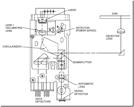
image

FIGURE 25.1 Drawing of the optical head in a typical magneto-optic disk drive. Shown is a split-optics design, which consists of a fixed set of components (the laser, detectors, and polarizing optics) and a movable system consisting of a beam bender and an objective lens that focuses the light on the disk. (Source: Asthana, P. 1994. Laser Focus World, Jan., p. 75. Penwell Publishing Co., Nashua, N.H. Used by permission.)

the divergence angles to be unequal in the directions parallel and perpendicular to the laser junction. The spatial profile of the laser beam some distance from the laser is thus elliptical.

The basic layout of the optical head of a magneto-optic drive is shown in Fig. 25.1. The laser is mounted in a heat sink designed to achieve an athermal response. The output from the laser diode is collimated by lens 1. A prismlike optical element called a circularizer is then used to reduce the ellipticity of the laser beam. The beam then passes through a polarizing beamsplitter, which reflects part (30%) of the beam toward a detector and transmits the rest toward the disk.

The output of the laser is linearly polarized in the direction parallel to the junction (which will be referred to as P-polarization). The ratio of the intensity of the P-polarization component of the emitted light to the ratio of the intensity in the S-polarization component is > 25:1. This polarizing beam splitter is designed to transmit 70% of the P-polarized light and 100% of the S-polarized light. The light that is reflected is incident on a light detector, which is part of a power servoloop designed to keep the laser at a constant power. Without a power servoloop, the laser power will fluctuate with time as the laser junction heats up, which can adversely affect the read performance.

The beam transmitted by the beam splitter travels to a turning (90◦) mirror, called a beam bender, which is mounted on a movable actuator. During track seeking operations, this actuator can move radially across the disk. The beam reflected by the turning mirror is incident on an objective lens (also mounted on the actuator), which focuses the light on the disk. This type of optical head design in which the laser, the detectors, and most of the optical components are stationary while the objective lens and beambender are movable is called a split optics design. In early optical drive designs, the entire optical head was mounted on a actuator and moved during seeking operations. This led to slow seek times (∼200 ms) because of the mass on the actuator. A split optics design, which is possible because coherent light can be made highly collimated, lowers the mass on the actuator and thus allows much faster seek times.

The size of the focal spot formed by the objective lens on the disk depends on the numerical aperture (NA) of the lens and the amount of overfill of the lens (i.e., the amount with which the diameter of the incident collimated beam exceeds the aperture of the objective lens). The numerical aperture is given by

NA = n sin θmax,

in which n is the refractive index of the lens and θmax is the incidence angle of a light ray focused through the margin of the lens. The beam of light incident on the objective lens usually has a Gaussian electric field (or intensity) profile. The profile of the focused spot is a convolution of the incident intensity profile and the aperture of the objective lens (Goodman, 1968). Overfilling the lens aperture reduces the size of the focused spot at the cost of losing optical energy outside the aperture and increasing the size of the side lobes. Optimization of the amount of overfill (Marchant, 1990) yields an approximate spot diameter of

image

in which λ is the wavelength of light and NA is the numerical aperture of the objective lens. The depth of focus z of the focal spot is given by z = 0.8λ/(NA)2.

The depth of focus defines the accuracy with which the objective lens position must be held with respect to the disk surface. The smaller the depth of focus, the less tolerance the system has for media tilt and the more difficult the job of the focus servosystem. Thus trying to reduce the spot size (always a goal as a smaller spot allows a higher storage density) by increasing the NA of the lens becomes impractical beyond an NA of about 0.6. The objective lens also acts as a collector lens for the light that is reflected from the disk. This reflected light, used for the servosystems and during reading, contains the readout information. The reflected light follows the incident path up to the fixed optical element. Beamsplitter 1 reflects all of the S polarized light and 30% of the P polarized light in the direction of the servo and data detectors.

The portion of the light that is transmitted by the beamsplitter is, unfortunately, focused by the col- limating lens back into the facet of the laser. This feedback light causes a number of problems in the laser, even though the net amount of feedback does not exceed about 7% of the output light for most magneto-optic media. Optical feedback affects the laser by causing the laser to mode hop randomly, which results in a random amplitude fluctuation in the output. This amplitude noise can be a serious problem and so techniques must be used to control the laser noise (such as injection of high-frequency current) or HFM (Arimoto, 1986). Increasing the HFM current in general can decrease the amount of noise, but as a practical matter, the injection current cannot be made arbitrarily large as it may then violate limits on allowable radiation from computer accessories. Optical feedback also decreases the threshold and increases the slope of the power-current (or PI) curve of the laser, but these effects are not really a problem.

The light reflected by beamsplitter 1 is further split by beamsplitter 2 into servo and data components. The light reflected by the beamsplitter is incident on the data detectors. For magneto-optic read back, two detectors are used in a technique known as differential detection (i.e., the difference in the signals incident on the two detectors is taken). The light transmitted through beamsplitter 2 is incident onto a special multielement servodetector and is used to generate the servosignals. The mechanism by which these signals are generated are the subject of the following discussion on the servosystem.

The Servosystem

The servosystem is what enables the focused laser spot to be positioned with accuracy onto any of the tracks on the disk and ensure that it can be moved to any track on the disk as required. The high track densities (18,000 tracks/in) on optical disks require that the laser spot position be controlled to within a fraction of a micrometer. To be able to move across the entire disk surface requires a large actuator, but such an actuator will be too massive to quickly respond to the rapid changes in the track position (due to run-out in the disk) as the disk spins. Therefore, a compound actuator consisting of a coarse actuator and a fine actuator is used to control the radial position of the laser beam on the disk. The fine actuator, which has a very low mass, can change the spot position rapidly over a limited range. The coarse actuator has a slower response, but has a much wider range of motion and is used for long seek operations. Optical disks have a continuous spiral groove (as in a phonograph record) to provide information on the relative track location.

In addition to tracking and seeking, the laser spot in an optical drive must be kept in perfect focus on the disk regardless of the motion of the disk (there can be quite a lot of vertical motion if the disk has tilt
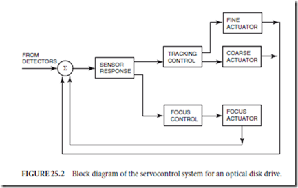
image

or is slightly warped). To do this, the objective lens must be constantly adjusted to correct for the axial motion of the disk surface as the media spins. The lens position is controlled by a focus servomechanism. Figure 25.2 shows a block diagram of an optical drive servocontrol system (combined tracking and focusing). The return beam contains information on the focus and position of the spot, which is processed by the servo detectors. The feedback signals derived from the detectors allow the system to maintain control of the beam.

The focus control system requires a feedback signal that accurately indicates the degree and direction of focus error (Braat and Bouwhuis, 1978; Earman, 1982). To generate a focus error signal, an astigmatic lens is used to focus onto a quadrant detector, a portion of the light reflected from the disk. In perfect focus, the focal spot is equally distributed on the four elements of the quad detector (as shown in Fig. 25.3). However, if the lens is not in focus, the focal spot on the detector is elliptical because of the optical properties of the astigmatic lens. The unequal distribution of light on the detector quadrants generates a focus error signal (FES).

This signal is normalized with respect to light level to make it independent of laser power and disk reflectivity. The focus actuator typically consists of an objective lens positioned by a small linear voice coil motor.

The coils are preferably mounted with the lens to reduce moving mass, while the permanent magnets are stationary. The lens can be supported by either a bobbin on a sliding pin or elastic flexures. The critical factors in the design are range of motion, acceleration, freedom from resonances, and thermal considerations.

Once the spot is focused on the active surface, it must find and maintain position along the desired track. This is the role of the tracking servo. The same quadrant detector that is used to generate the focus signal can be used to generate the tracking error signal (TES). The beam returning from the disk contains first-order diffraction components; their intensity depends on the position of the spot on the tracks and varies the light falling along one axis of the quadrant detector. The TES is the normalized difference of the current from the two halves of the detector, and it peaks when the spot passes over the cliff between a land and groove (Mansuripur, 1987; Braat and Bouwhuis, 1978).

As a matter of terminology, the seek time usually refers to the actual move time of the actuator. The time to get to data, however, is called the access time which includes the latency of the spinning disk in addition

imageFIGURE 25.3 Focus control system: (a) the quad detector, (b) the spot of light focused on the quad by the astigmatic lens (circular implies objective lens is in focus), and (c) the spot of light on the quad when the objective lens is out of focus.

to the seek time. For example, a drive spinning a disk at 3600 rpm has a latency of (0.5 × (60/3600)) s or 8 ms. Thus, a 3600-rpm drive with a seek time of 30 ms will have an access time of 38 ms. The standard

way to measure seek time is 1/3 of the full stroke of the actuator (i.e., the time it takes to cover 1/3 of the isk). This is a historical artifact from the times of early hard disk drives.

The ability to accurately follow the radial and axial motions of the spinning disk results directly from he quality of the focus and tracking actuators. To reject the errors due to shock, vibration, and media unout, the servosystem must have high bandwidth. The limitation to achieving high bandwidth is usually he resonance modes of the actuator. As the actuators are reduced in size, the frequencies of the resonances ecome higher and the achievable bandwidth of the system rises. Servosystems in optical drives face dditional challenges because they have to handle removable media, which has variations between different isks (such as media tilt).

Optical Recording and Read Channel

A schematic block diagram of the functions in an optical drive is shown in Fig. 25.4. The SCSI controller handles the flow of information to and from the host (including commands). The optical disk controller is a key controller of the data path. It interprets the commands from the SCSI controller and channels data appropriately through the buffer random access memory (RAM) to the write channel, or from the read channel to the output. The drive control microprocessor unit controls, through the logic gate arrays, all the functions of the optical drive including the servo control, spindle motor, actuators, laser driver, etc.

Data that are input to the drive over the SCSI for recording are first broken up into fixed block sizes (of, for example, 512 kilobyte or 1024 kilobytes length) and then stored in the data buffer RAM. Magneto-optic, phase-change, and WORM drives can be classified as fixed block architecture technologies in which data blocks are recorded much like in hard drives (Marchant, 1990). Blocks of data can be placed anywhere on the disk in any sequence. The current CD recordable drive is, on the other hand, an example of a non-fixed block architecture (because its roots are in CD audio). In common CD-R drives, input data are recorded sequentially (like a tape player) and can be of any continuous length.

Error correction and control (ECC) bytes are added to each block of data. Optical drives use Reed– Solomon codes, which are able to reduce the error rate from 1E-5 to about 1E-13 (Golomb, 1986). After the addition of ECC information, the data are encoded with run length limited (RLL) modulation codes (Tarzaiski, 1983; Treves and Bloomberg, 1986) in order to increase efficiency and improve detection. Special characters are inserted in the bit stream such as a synchronization character to tell where the data begins. All in all, the overhead required to store customer data is about 20%.

In most current optical drives, recording is based on pulse position modulation (PPM) techniques. In basic PPM recording, the presence of a mark signifies a one and the absence signifies a zero bit. Thus, a 1001 bit sequence would be recorded as mark-space-space-mark. In pulse width modulation (PWM) recording, the edges of the mark represent the one bits (Sukeda et al., 1987). Thus a 1001 bit sequence would be recorded as a single mark of a certain size. A longer bit sequence such as 100001 would be represented by a longer mark, hence the term pulse width modulation. The use of pulse width modulation allows a higher linear density of recording than pulse position modulation.

A comparison of PWM recording with the current technique of PPM is shown in Fig. 25.5. It is more difficult to implement PWM technology (a more complicated channel is required), and PWM writing has greater sensitivity to thermal effects. Thus implementing PWM is a challenging task for drive vendors.

On readback, the light reflects from the disk and travels to a photodetector (or two detectors in the case of magneto-optic drives). For WORM, phase-change, and CD-R disks, the signal is intensity modulated and thus can be converted to current from the detectors and amplified prior to processing. The WORM, phase-change, and CD-R disks have a high contrast ratio between mark and no-mark on the disk and thus provide a good signal-to-noise ratio. In magneto-optic drives, the read signal reflected off the disk is not intensity modulated but polarization modulated. Thus polarization optics and the technique of differential detection must be used to convert the polarization modulation to intensity modulation (as is discussed later in the section on magneto-optic recording).
image

FIGURE 25.4 A functional block diagram of an optical disk drive describing the key electrical functions and interfaces. Some of the abbreviations are: VFO is the variable field oscillator, which is used to synchronize the data, RD amp is the read signal amplifier, WR amp is the write signal amplifier, PD fixed is the photodetextor assemply, and LD head is the laser diode.

To extract the 1s and 0s from the noisy analog signal derived from the photodetectors, optical drives use a number of techniques, such as equalization, which boosts the high frequencies and thus provides greater discrimination between spots. Using an analog-to-digital converter, the analog data signal is converted into channel bits. The channel bits are converted back into customer data bytes using basically the reverse of the encoding process. The data is clocked into the decoder, which removes the modulation code. The remaining special characters are removed from the data, which is then fed into the ECC alignment buffer to correct any errors (up to 40 bytes long). Once data has been read from the disk, it is stored in a RAM buffer and then output to whatever readout device is hooked by SCSI to the drive. With this basic understanding
image

FIGURE 25.5 Schematic showing the mark spacing for PPM and PWM recording. The PPM recording is used in most current optical drives. The PWM recording increases capacity by as much as 50% and will be used in almost all forthcoming writable optical drives. PWM recording, however, requires much tighter tolerances than PPM recording.

of how data is recorded on a spinning disk, we can turn to the specific items such as recording physics that delineate the various recording technologies.

Phase-Change Recording

Phase-change recording takes advantage of the fact that certain materials can exist in multiple metastable i.e. normally stable) crystalline phases, each of which have differing optical properties (such as reflectivity).

Thermal energy (as supplied by the focused beam of a high-power laser) above some threshold can be used o switch from one metastable state to another (Ovshinsky, 1970; Takenaga et al., 1983). Energy below the witching threshold should have no effect. In this way a low-power focused spot can be used to read out he recorded information without affecting it.

To achieve this kind of multiple metastable states, phase-change materials typically are a mixture of everal elements such as germanium, tellurium, and antimony (Ge2Sb2Te5). Phase-change materials are available that are suited for either rewritable or write-once recordings. In an erasable material, recording is affected by melting the material under the focused spot and then cooling it quickly enough to freeze it in an amorphous phase. Rapid cooling is critical and, thus, the design of the heat sinking capability of the material is important.

Erasure of the phase-change material is achieved by an annealing process, that is, heating the material to just below the melting point for a long enough period to recrystallise the material and erase any amorphous marks.

The fact that phase-change materials are a mixture of several materials makes recyclability difficult to achieve. The melting/annealing processes increase phase segregation and thus reduce the number of cycles that can be achieved. Early phase-change materials could only achieve a few thousand cycles, which is one of the primary reasons they were passed over by many companies in favor of magneto-optical products when rewritable drives were being introduced. However, the cyclability of phase-change materials has increased substantially.

The advantage of phase-change recording over magneto-optic recording is that a simpler head design is possible (since no bias magnet and fewer polarizing optics are needed). The disadvantages include the fact
image

FIGURE 25.6 Permanent WORM recording provides the highest level of data security available in a removable storage device. In ablative WORM recording, marks are physically burned into the material. In phase-change worm, the recording process is a physical change in the material, which results in a change in reflectivity.

that there is less standardization support for the phase-change format, and fewer companies produce the drives. For the consumer this means there is less interchange with phase-change than with magneto-optic.

Worm Technology

The earliest writable optical drives were, in fact, WORM drives, and although the rewritable drive is more popular for daily storage needs, the WORM technology has a clear place in data storage because it allows permanent archiving capability.

There are a number of different types of write-once technologies that are found in commercial products. Ablative WORM disks consist of tellurium-based alloys. Writing of data is accomplished by using a high- powered laser to burn a hole in the material (Kivits et al., 1982). A second type of WORM material is what is known as textured material, such as in a moth’s eye pattern. The actual material is usually a platinum film. Writing is accomplished by melting the textured film to a smooth film and thus changing the reflectivity. Phase-change technology provides a third type of WORM technology using materials such as tellurium oxide. In the writing process, amorphous (dark) material is converted to crystalline (light) material by application of the heat from a focused laser beam (Wrobel et al., 1982). The change cannot be reversed. A comparison of phase-change and ablative WORM recording is shown schematically in Fig. 25.6.

Magneto-Optic Technology

In a magneto-optic drive, data recording is achieved through a thermomagnetic process (Mayer, 1958), also known as Curie point writing as it relies on the threshold properties of the Curie temperature of magnetic materials. In this process, the energy within the focused optical spot heats the recording material past its Curie point (about 200◦C), a threshold above which the magnetic domains of the material are susceptible to moderate (about 300 G) external magnetic fields. Application of an external magnetic field is used to set the state of the magnetization vector (which represents the polarization of the magnetic domains) in the heated region to either up (a one bit) or down (a zero bit). When the material is cooled to below the Curie point this orientation of the magnetic domains is fixed. An illustration of the magneto-optic recording process is given in Fig. 25.7. This recording cycle has been shown to be highly repeatable (>1 million cycles) in any given region without degradation of the material. This is an important aspect if the material is to be claimed as fully rewritable.

In any practical recording process, it is necessary to have a sharp threshold for recording. This ensures the stability of the recorded information both to environmental conditions as well as during readout. Thermo-magnetic recording is an extremely stable process. Unless heated to high temperatures (>100◦C), the magnetic domains in magneto-optic recording films are not affected by fields under several kilogauss
image

in strength (in comparison, the information stored on a magnetic floppy is affected by magnetic fields as low as a 100 G). The coercivity of a magneto-optic material remains high until very close to the Curie temperature. Near the Curie temperature (about 200◦C), the coercivity rapidly drops by two or three orders of magnitude as the magnetic domain structure becomes disordered.

Readout of the recorded information can safely be achieved with a laser beam of about 2-mW power at the disk, a power level which is high enough to provide good signal strength at the detectors, but low enough not to affect the recorded information because any media heating from it is far below the Curie threshold. During readout, the magnetic state of the recorded bits of information is sensed through the polar-Kerr effect by a low-power linearly polarized readout beam. In this effect the plane of polarization of the light beam is rotated slightly (0.5◦) by the magnetic vector. The direction of rotation, which defines whether the bit is a one or a zero, is detected by the readout detectors and channel. Although the tiny amount of Kerr rotation results in a very small amount of signal modulation riding on a large DC bias, the technique of differential detection permits acceptable signal-to-noise ratio (SNR) to be achieved.

The output signal in an MO recording system is the signal from the light falling on one detector minus the signal from the light falling on the other detector. By placing a polarizing beamsplitter at 45◦ to the incident polarization, the two data detectors get the signals (Mansuripur, 1982)

image

in which d1 and d2 refer to the detector signals, I0 is the incident intensity, and θk /2, the rotation angle, is assumed to be small. The readout signal is taken as

image

As can be seen, this signal does not contain intensity noise from either the laser or from reflectivity variations of the disk. But the signal is very sensitive to polarization noise, which may be introduced by polarization

sensitive diffraction, by substrate birefringence effects, by inhomogeneities in the magnetooptic films, or by other polarization sensitive components.

Early MO recording media, such as manganese bismuth (MnBi) thin films (Chen et al., 1968), were generally crystalline in nature. The magnetic domains followed the crystalline boundaries and thus were irregular in shape (Marchant, 1990). The crystalline nature of the films caused optical scattering of the readout signal, and the irregular domains led to noise in the recorded signal. The combination degraded the SNR sufficiently to make polycrystalline magneto-optic media impractical.

The discovery in 1976 of magneto-optic materials based on the rare earth/transition metal (RE/TM) alloys (Choudhari et al., 1976) provided a practical material system for rewritable magneto-optic recording. These materials were amorphous and thus allowed acceptable signal-to-noise ratio to be obtained. Most commercial magneto-optic films today are based on terbium iron cobalt (TbFeCO).

Compact Disk-Recordable (CD-R)

The writable version of the popular CD-R disk looks very much like a stamped CD-ROM disk, and can be played in most CD-ROM players.

One of the reasons why CD-audio and CD-ROM have become so successful is the strict, uniform standards that all of the manufacturers of these products have adhered to. The standards were drawn up by Philips and Sony and are described by the colors of the books that they were first printed in. The standards describing CD-audio are found in the Red Book, those describing CD-ROM are found in the Yellow book, and those describing CD-R are found in the Orange Book. These books describe the physical attributes that the disks must meet (such as reflectivity, track pitch, etc.), as well as they layout of recorded data (Bouwhuis et al., 1985).

In prerecorded CD-ROM disks, the information is stamped as low reflectivity pits on a high reflectivity background. The disk has a reflectivity of 70% (achieved by using an aluminum layer), whereas the pits have a reflectivity of 30% (these reflectivity specifications have been defined in the Red Book). The CD-ROM drive uses this difference in reflectivity to sense the information stamped on the disk. To be compatible with CD-ROM readers, a CD-R disk must also use this reflectivity difference when recording data. To accomplish this, a CD-R disk is coated with an organic polymer that can change its local reflectivity permanently upon sufficient heating by a laser spot. The structure of a CD-R disk is shown in Fig. 25.8.

When the organic dye polymer is locally heated by the focused spot of a laser beam, polymeric bonds are broken or altered resulting in a change in the complex refractive index within the region. This refractive index change results in a change in the material reflectivity. There are a half-dozen organic dye polymers that are commercially being used. Two examples are phthalocyanine and poly-methane cyanine.

Like the CD-ROM drives, the CD-R drives have relatively low performance (when compared with optical or hard drives). The seek times are on the order of a few hundred milliseconds, whereas the maximum
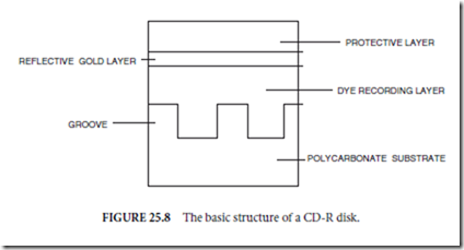
image

data rate for a 4X speed drive is about 600 kilobytes/s. The seek time is slow because the CD-R drives spin the disks in constant linear velocity (CLV) mode as defined in the Red Book standards. Constant linear velocity means that the disk rotation speed varies with the radius at which the read head is positioned in such a way as to ensure that the linear velocity is constant with radius.

Pure data devices such as hard disks and optical WORM drives, however, can handle constant angular velocity (CAV) operation in which the linear velocity and data rate increase with radial position. The disadvantage of CLV operation is that it results in a very slow access time. When a seek of the optical head is performed, the motor speed has to be adjusted according to the radial position of the head. This takes time and thus lengthens the seek operation to 250–300 ms. In contrast, constant angular velocity devices like optical WORM disks have seek times on the order of 40 ms.

The roots of CD-R are found in audio CD, and thus some of the parameters, recording formats, and performance features are based on the Red Book standard (which has tended to be a handicap). The CD format (Bouwhuis et al., 1985) is not well suited for random access block oriented recording. The CD format leads to a sequential recording system, much like a tape recorder.

Recording Modes of CD-R

To understand the attributes and limitations of CD-R, it is important to understand the various recording modes that it can operate in. For fixed block architecture devices, the question of recording modes never comes up as there is only one mode, but in CD-R, there are four modes (Erlanger, 1994).

The four recording methods in CD-R drives are

  • Disk-at-once (or single session)
  • track-at-once
  • Multisession
  • Incremental packet recording

In disk-at-once recording, one recording session is allowed on the disk, whether it fills up the whole disk or just a fraction of the disk. The data area in a single session disk consists of a lead-in track, the data field, and a lead out track. The lead-in track contains information such as the table of contents (TOC). The lead-in and lead-out are particularly important for interchange with CD-ROM drives. In single session writing, once the lead-in and lead-out areas are written, the disk is considered finalized and further recording (even if there are blank areas on the disk) cannot take place. After the disk is finalized, it can be played back on a CD-ROM player (which needs the lead-in and lead-out tracks present just to read the disk).

Having just the capability of recording a single session can be a quite a limitation for obvious reasons, and so the concept of multisession recording was introduced. An early proponent of multisession recording was Kodak, which wanted multisession capability for its photo-CD products. In multisession recording, each session is recorded with its own lead-in and lead-out areas. Multisession recorded disks can be played back in CD-ROM drives that are marked multisession compatible (assuming that each session on the disk has been finalized with lead-in and lead-out areas). Unfortunately, the lead-in and lead-out areas for each session take up lots of overhead (about 15 megabytes). With this kind of overhead, the ultimate maximum number of sessions that can be recorded on a 650 megabyte disk is 45 sessions.

Rather than do multisession recording, the user may choose track-at-once recording. In this type of recording, a number of tracks (which could represent distinct instances of writing) could be written within each session. The maximum number of tracks that can be written on the whole disk is 99. However, the disk or session must be finalized before it can be read on a CD-ROM drive.

Because of the way input data are encoded and spread out, it is imperative to maintain a constant stream of information when recording. If there is an interruption in the data stream, it affects the whole file being recorded (not just a sector as in MO or WORM drives). If the interruption is long enough, it will cause a blank region on the disk and will usually lead to the disk being rendered useless.

Many of these problems or inconveniences can be alleviated through a recording method called packet recording. In packet recording, the input data are broken up into packets of specified size (for example 128

kilo-bytes or 1 megabyte). Each packet consists of a link block, four run-in blocks, the data area, and two run-out blocks. The run-in and run-out blocks help delineate packets and allow some room for stitching, that is, provide some space for overlap if perfect synching is not achieved when recording an adjacent packet in a different CD-R drive.

Packet recording has several advantages. To begin with, there is no limit to the number of packets that can be recorded (up to the space available on the disk, of course), and so limitations imposed by track-at- once, multisession, or disk-at-once can be avoided. Also, if the packet size is smaller than the drive buffer size (as is likely to be the case), a dedicated hard drive is not needed while recording. Once the packet of information has been transferred to the drive buffer, the computer can disengage and do other tasks while the CD-R drive performs the recording operation.

With the advent of packet recording, CD-R technology becomes much more flexible than in the past and thus more attractive as a general purpose removable data storage device. It can be used for backup purposes as well the storage of smaller files. However, there is a problem of interchange with CD-ROM players. Some CD-ROM players cannot read a CD-R disk that has been packet written because they post a hard error when they encounter the link block at the beginning of each packet. Packet written CD-R disks can be read on CD-R drives and on CD-ROM drives that are packet enabled.

Optical Disk Systems
Disks

An important component of the optical storage system is, of course, the media cartridges. In fact, the greatest attraction of optical storage is that the storage media is removable and easily transported, much like a floppy disk. Most of the writable media that is available comes in cartridges of either 3.5- or 5.25-in. form factors. An example of the 5.25-in. cartridge is shown in Fig. 25.9. The cartridge has some sensory holes to allow its media type to be easily recognized by the drive. The tracks on the media are arranged in a spiral fashion. The first block of data is recorded on the innermost track (i.e., near the center). Recordable CD media is cartridgeless and is played in CD-R/CD-ROM drives either using a caddy or through tray loading (like audio CD players).

Cartridged media has been designed to have a long shelf and archival life (without special and expensive environmental control) and to be robust enough to survive the rigors of robotic jukeboxes and customer handling. Magneto-optic and WORM media is extremely stable and so data can be left on the media with great confidence (Okino, 1987). A chart showing projected lifetimes (after accelerated aging) of IBM WORM media is given in Fig. 25.10, which indicates that the lifetimes for 97.5% of the media surfaces for shelf and archival use are projected to exceed 36 and 510 years, respectively, for storage at 30◦C/80%
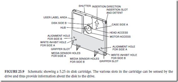
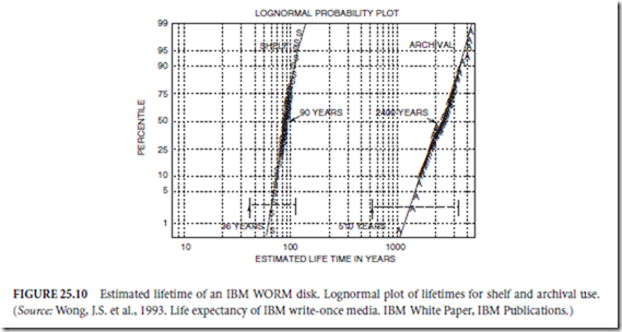
image


image

relative humidity. Shelf life is the length of time that data can be effectively written, whereas archival life is the length of time that data can be effectively read.

Optical media is perhaps the most stable digital storage technology: magnetic drives are prone to head crashes, tape deteriorates or suffers from print through (in which information on one layer is transferred to another layer in the tightly wound tape coil), and paper or microfiche also deteriorate with time (Rothenberg, 1995).

Automated Optical Storage Systems
Optical drives can be extended to automated storage systems, which are essentially jukeboxes consisting of one or more optical drives and a large number of optical disk cartridges. Optical libraries can provide on-line, direct-access, high-capacity storage.
Applications of Optical Library Systems

Optical library systems fit well into a large computer- based environment, such as client-server systems, peer-to-peer local area networks, or mainframe- based systems. In such environments, there is a distinct storage hierarchy based on cost/access trade-

off of various types of data. This hierarchy is shown schematically in Fig. 25.11 as a pyramid. The highest section of the pyramid contains the highest performance and highest cost type of memory. The most inexpensive (on a cost/megabyte) basis and lowest performance is that of tape. Optical libraries are an important part of this segment because they provide storage with performance capabilities approaching that of magnetic, but at a cost approaching that of tape.

An optical library contains a cartridge transport mechanism called an autochanger. The autochanger moves optical cartridges between an input/output slot (through which cartridges can be inserted into the library), the drives (where the cartridges are read or written), and the cartridge storage cells.
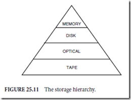
image

Sophisticated storage systems provide a hierarchical storage management capability in which data are automatically migrated between the various layers of the pyramid depending on the access needs of the data. For example, a telephone company can keep current billing information on magnetic storage, whereas billing information older than a month can be stored in optical libraries, and information older than six months can be stored on tape. It does not make sense to keep data that the system does not frequently access on expensive storage systems such as semiconductor memory or high erformance magnetic drives.

One of the applications for which automated optical storage is ideally suited is  ocument imaging. Document imaging directly addresses the substantial paper management problem in society today.

The way we store and manage paper documents has not changed significantly in over a century, and largely does not take advantage of the widespread availability of computers in the workplace. Trying to retrieve old paper documents is one of the most inefficient of business activities today (some businesses have stockrooms full of filing cabinets or document boxes). The way information is currently stored can be represented by a pyramid (as shown in Fig. 25.12), in which paper accounts for almost all of the document storage.
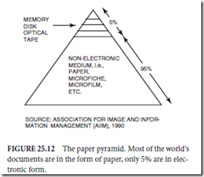
image

An application aimed squarely at re-enginee- ring the way we handle and store documents is document imaging. In document imaging, documents are scanned onto the computer and stored as computer readable documents. Storing documents in computer format has many advantages, including rapid access to the information. Recall of the stored documents is as easy as typing in a few key search words. Document imaging, however, is very storage intensive and, thus, a high-capacity, low-cost storage technology is required, ideally with fast random access. Optical storage is now recognized as the optimal storage technology in document imaging. Optical libraries can accommodate the huge capacities required to store large numbers of document images (text and/or photos), and optical drives can provide random access to any of the stored images. Figure 25.13 illustrates the equivalent storage capacity of a single 1.3 gigabyte optical disk.
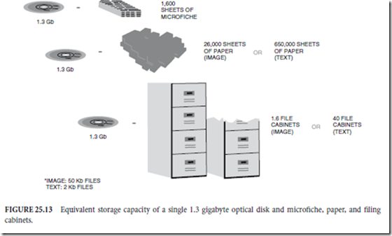
image 

Future Technology and Improvements in Optical Storage

Optical drives and libraries, like anyhigh-technology products, will see two types of improvement processes. The first is an incremental improvement process in which quality and functionality will continuously improve. The second is a more dramatic improvement process in which disk capacity and drive performance will improve in distinct steps every few years.

For the library, the improvements will be in the speed of the automated picker mechanism as well as the implementation of more sophisticated algorithms for data and cartridge management. Most of the improvements in the library systems will arise out of improvements in the drives themselves.

For the optical drive, the incremental improvement process will concentrate on the four core technology elements: the laser, the media, the recording channel, and the optomechanics. The laser will see continual improvements in its beam quality (reduction of wavefront aberrations and astigmatism), lifetime (which will allow drive makers to offer longer warranty periods), and power (which will allow disks to spin faster). The media will see improvements in substrates (reduction of tilt and birefringence), active layers (improved sensitivity), and passivation (increased lifetimes). The optics and actuator system will see improvements in the servosystem to allow finer positioning, reductions in noise, smaller optical components, and lighter actuators for faster seek operations. The recording channel and electronics will see an increase in the level of electronics integration, a reduction in electronic noise, the use of lower power electronics, and better signal processing and ECC to improve data reliability. One of the paramount directions for improvement will be in the continuous reduction of cost of the drives and media. This step is necessary to increase the penetration of optical drives in the marketplace.

In terms of radical improvements, there is a considerable amount of technical growth that is possible for optical drives. The two primary directions for future work on optical drives are (1) increasing capacity and (2) improving performance specifications (such as data rate and seek time). The techniques to achieve these are shown schematically in Fig. 25.14.

The performance improvements will include spinning the disk at much higher revolutions per minute to get higher data rates, radically improving the seek times for faster access to data, and implementing direct overwrite and immediate verify techniques to reduce the number of passes required when recording. Finally, the use of parallel recording (simultaneous recording or readback of more than one track), either through the use of multielement lasers or through special optics, will improve the data rates significantly.

In optical disk products, higher capacities can only be achieved by higher areal densities since the size of the disk cannot increase from presently established standard sizes. There are a number of techniques that are being considered for improving the storage capacity of optical drives. These include

  • ✁ Use of shorter wavelength lasers or superresolution techniques to achieve  maller spot sizes
  • Putting the data tracks closer together for greater areal density
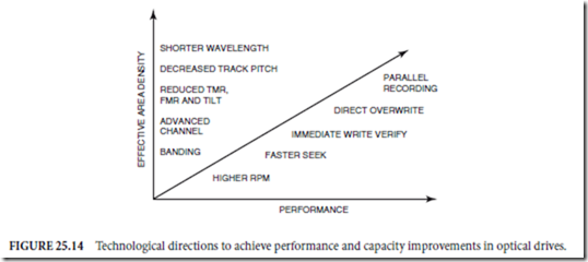
image

  • Reducing the sensitivity to focus misregistration (FMR) (i.e., misfocus) and tracking misregistration (TMR) (i.e., when the focused spot is not centered on the track)
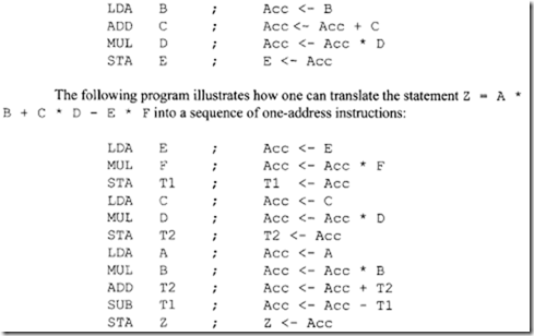
  • Reducing the sensitivity to media tilt

Finally, improvements in the read channel such as the use of partial-response-maximum-likelihood (PRML) will enable marks in high-density recording to be detected in the presence of noise.

Acknowledgments

The author is grateful to two IBM Tucson colleagues: Blair Finkelstein for discussions and suggestions on the read channel section and Alan Fennema for writing some of the paragraphs in the servo section.

Defining Terms

Compact disk erasable/compact disk recordable (CD-E/CD-R): These define the writable versions of the compact disk. CD-E is a rewritable media and CD-R is a write-once media.

Data block size: The data that is to be recorded on an optical disk is formatted into minimum block sizes. The standard block size, which defines a single sector of information, is 512 byte. Many DOS/windows programs expect this block size. If the block size can be made larger, storage usage becomes more efficient. The next jump in block size is 1024 byte, often used in Unix applications.

Device driver: This is a piece of software that enables the host computer to talk to the optical drive. Without this piece of software, you cannot attach an optical drive to a PC and expect it to work. As optical drives grow in popularity, the device driver will be incorporated in the operating system itself. For example, the device driver for CD-ROM drives is already embodied in current operating systems.

Error correction and control (ECC): These are codes (patterns of data bits) that are added to raw data bits to enable detection and correction of errors. There are many types of error correcting codes. Compact disk drives, for example, use cross interleaved Reed–Solomon codes.

Magneto-optical media: An optical recording material in which marks are recorded using a thermomagnetic process. That is, the material is heated until the magnetic domains can be changed by the application of a modes magnetic field. This material is rewritable.

Optical jukebox: This is very similar to a traditional jukebox in concept. A large number of disks are contained in a jukebox and can be accessed at random for reading or writing.

Phase-change media: An optical recording material consisting of an alloy that has two metastable phases with different optical properties. Phase-change media can be rewritable or write-once.

Pulse-position modulation (PPM): A recording technique in which a mark on the disk signifies a binary 1 and its absence signifies a binary 0. A 1001 bit sequence is mark-space-space-mark.

Pulse-width modulation (PWM): A recording technique in which the edges of the mark represent the ones and the length of the mark represents the number of zeros. Thus, a 1001 sequence is represented by one mark.

Seek time/access time: The two terms are often used interchangeably, which is incorrect. The seek time is, by convention, defined as the length of time taken to seek across one-third of the full stroke of the actuator (which is from the inner data band to the outer data band on the disk). The access time is the seek time plus some latency for settling of the actuator and for the disk to spin around appropriately. The access time really states how quickly you can get to data.

Servosystem: The mechanism, which through feedback and control, keeps the laser beam on track and in focus on the disk—no easy task on a disk spinning at 4000 rpm.

Tracking: The means by which the optical stylus (focused laser beam) is kept in the center of the data tracks on an optical disk.

References

Arimoto, A. et al. 1986. Optimum conditions for high frequency noise reduction method in optical videodisk players. Appl. Opt. 25(9):1.

Asthana, P. 1994. A long road to overnight success. IEEE Spectrum 31(10):60.

Bouwhuis, G., Braat, J., Huijser, A., Pasman, J., van Rosmalem, G., and Schouhamer Immink, K. 1985.

Principles of Optical Disk Systems. Adam Hilger, Bristol, England, UK.

Braat, J. and Bouwhuis, G. 1978. Position sensing in video disk read-out. Appl. Opt. 17:2013.

Chen, D., Ready, J., and Bernal, G. 1968. MnBi thin films: Physical properties and memory applications.

J. Appl. Phys. 39:3916.

Choudhari, P., Cuomo, J., Gambino, R., and McGuire, T. 1976. U.S. Patent #3,949,387.

Earman, A. 1982. Optical focus servo for optical disk mass data storage system application. SPIE Proceedings

329:89.

Erlanger, L. 1994. Roll your own CD. PC Mag. (May 17):155.

Golomb, S. 1986. Optical disk error correction. BYTE (May):203.

Goodman, J. 1968. Introduction to Fourier Optics. McGraw-Hill, San Francisco.

Inoue, A. and Muramatsu, E. 1994. Wavelength dependency of CD-R. Proceedings of the Optical Data

Storage Conference. Optical Society of America, May, p. 6.

Kivits, P., de Bont, R., Jacobs, B., and Zalm, P. 1982. The hole formation process in tellerium layers for

optical data storage. Thin Solid Films 87:215.

Mansuripur, M., Connell, G., and Goodman, J.W. 1982. Signal and noise in magneto-optical readout. J.

Appl. Phys. 53:4485.

Mansuripur, M. 1987. Analysis of astigmatic focusing and push-pull tracking error signals in magneto-

optical disk systems. Appl. Opt. 26:3981.

Marchant, A. 1990. Optical Recording. Addison-Wesley, Reading, MA.

Mayer, L. 1958. Curie point writing on magnetic films. J. Appl. Phys. 29:1003.

Okino, Y. 1987. Reliability test of write-once optical disk. Japanese J. Appl. Phys. 26.

Ovshinsky, S. 1970. Method and apparatus for storing and retrieving information. U.S. Patent #3,530,441.

Rothenberg, J. 1995. Ensuring the longevity of digital documents. Sci. Am. (Jan.).

Sukeda, H., Ojima, M., Takahashi, M., and Maeda, T. 1987. High density magneto-optic disk using highly

controlled pit-edge recording. Japanese J. Appl. Phys. 26:243.

Takenaga, M. et al. 1983. New optical erasable medium using tellerium suboxide thin film. SPIE Proc.

420:173.

Tarzaiski, R. 1983. Selection of 3f (1,7) code for improving packaging density on optical disk recorders.

SPIE Proc. 421:113.

Treves, D. and Bloomberg, D. 1986. Signal, noise, and codes in optical memories. Optical Eng. 25:881.

Wrobel, J., Marchant, A., and Howe, D. 1982. Laser marking of thin organic films. Appl. Phys. Lett. 40:928.

Further Information

There are a number of excellent books that provide an overview of optical disk systems. A classic is Optical Recording by Alan Marchant (Addison-Wesley, Reading, MA, 1990), which provides an overview of the various types of recording as well as the basic functioning of an optical drive. A more detailed study of optical disk drives and their opto-mechanical aspects is provided in Principles of Optical Disc Systems by

G. Bouwhuis, J. Braat, A. Huijser, J. Pasman, G. van Rosmalen, and K. Schouhamer Immink (Adam Hilger Ltd., Bristol, England, 1985). An extensive study of magneto-optical recording is presented in The Physical Properties of Magneto-Optical Recording by Masud Mansuripur (Cambridge University Press, London, 1994).

For recent developments in the field of optical storage, the reader is advised to attend the meetings of the International Symposium on Optical Memory (ISOM) or the Optical Data Storage (ODS) Conferences (held under the auspices of the IEEE or the Optical Society of America).

For information on optical storage systems and their applications, a good trade journal is the Computer Technology Review. Imaging Magazine usually has a number of good articles on the applications of optical libraries to document imaging, as well as periodic reviews of commercial optical products.