7.1 Desi n of the CPU
The CPU contains three elements: registers, the ALU (Arithmetic Logic Unit), and the control unit. These topics are discussed next. Verilog and VHDL descriptions along with simulation results of a typical CPU are provided in Appendices I and J respectively.
7.3.1 Register Design
The concept of general-purpose and flag registers is provided in Chapters 5 and 6. The main purpose of a general-purpose register is to store address or data for an indefinite period of time. The computer can execute an instruction to retrieve the contents of this register when needed. A computer can also execute instructions to perform shift operations on the contents of a general-purpose register. This section includes combinational shifter design and the concepts associated with barrel shifters.
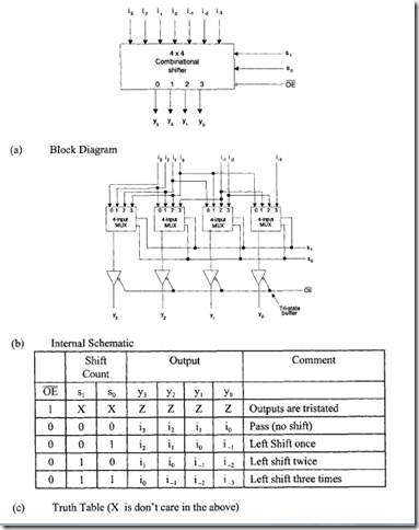
A high-speed shifter can be designed using combinational circuit components such as a multiplexer. The block diagram, internal organization, and truth table of a typical combinational shifter are shown in Figure 7.7. From the truth table, the following equations can be obtained:
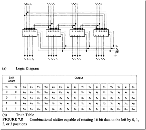
 The 4 x 4 shifter of Figure 7.7 can be expanded to obtain a system capable of rotating 16-bit data to the left by 0, 1, 2, or 3 positions, which is shown in Figure 7.8.
This design can be extended to obtain a more powerful shifter called the barrel
FIGURE7.7 4 x 4 combinational shifter
shifter. The shift is a cycle rotation, which means that the input binary information is shifted in one direction; the most significant bit is moved to the least significant position.
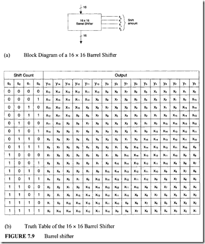
The block-diagram representation of a 16 x 16 barrel shifter is shown in Figure 7.9. This shifter is capable of rotating the given 16-bit data to the left by n positions, where 0 s n s 15. Figure 7.9 shows the truth table representing the operation of the shifter. The barrel shifter is an on-chip component for typical 32-bit and 64-bit microprocessors.
Addition is the basic arithmetic operation performed by an ALU. Other operations such as subtraction and multiplication can be obtained via addition. Thus, the time required to add two numbers plays an important role in determining the speed of the ALU.
The basic concepts of half-adder, full adder, and binary adder are discussed in Section 4.5 .1. The following equations for the full-adder were obtained. Assume xi = x, yi
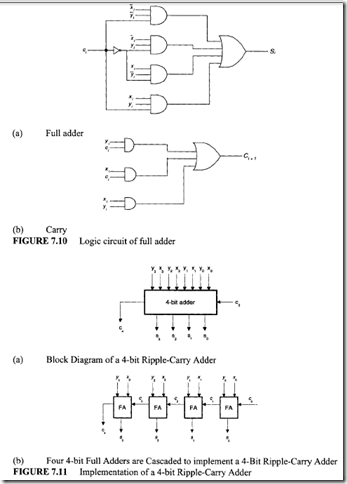
The logic diagrams for implementing these equations are given in Figure 7.10.
As has been made apparent by Figure 7.10, for generating Ci+I from ci, two gate delays are required. To generate Si from ci, three gate delays are required because ci must be inverted to obtain ci. Note that no inverters are required to get X: or .Y; from xi or yi, respectively, because the numbers to be added are usually stored in a register that is a collection of flip-flops. The flip-flop generates both normal and complemented outputs.
For the purpose of discussion, assume that the gate delay is ll. time units, and the actual value of ll. is decided by the technology. For example, if transistor translator logic (TTL) circuits are used, the value of ll. will be 10 ns.
By cascading n full adders, an n-bit binary adder capable of handling two n-bit operands (X and Y) can be designed. The implementation of a 4-bit ripple-carry or binary adder is shown in Figure 7.11. When two unsigned integers are added, the input carry, c0, is always zero. The 4-bit adder is also called a "carry-propagate adder" (CPA), because the carry is propagated serially through each full adder. This hardware can be cascaded to obtain a 16-bit CPA, as shown in Figure 7.12; c0 = 0 or 1 for multiprecision addition.
Although the design of an n-bit CPA is straightforward, the carry propagation
time limits the speed of operation. For example, in the 16-bit CPA (see Figure 7.12), the
 addition operation is completed only when the sum bits s0 through s15 are available.
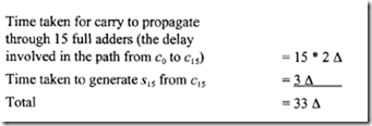
To generate s15, c15 must be available. The generation of c15 depends on the availability of c 14, which must wait for c13 to become available. In the worst case, the carry process propagates through 15 full adders. Therefore, the worst-case add-time of the 16-bit CPA can be estimated as follows:
FIGURE 7.12 Implementation of a 16-bit adder using 4-Bit Adders as Building Blocks
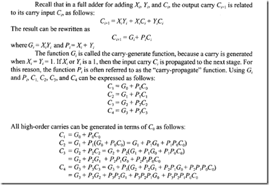
If Δ = 10 ns, then the worst-case add-time of a 16-bit CPA is 330 ns. This delay is prohibitive for high-speed systems, in which the expected add-time is typically less than 100 ns, which makes it necessary to devise a new technique to increase the speed of operation by a factor of 3. One such technique is known as the "carry look-ahead." In this approach the extra hardware is used to generate each carry (c;, i > 0) directly from c0• To be more practical, consider the design of a 4-bit carry look-ahead adder (CLA). Let us see how this may be used to obtain a 16-bit adder that operates at a speed higher than the 16-bit CPA.
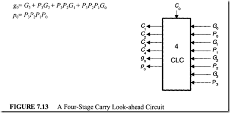
Therefore C1 , C2 , C3, and C4 can be generated directly from C0 • For this reason, these equations are called "carry look-ahead equations," and the hardware that implements these equations is called a "4-stage look-ahead circuit" (4-CLC). The block diagram of such circuit is shown in Figure 7.13.
The following are some important points about this system:
-
A 4-CLC can be implemented as a two-level AND-OR logic circuit (The first level consists of AND gates, whereas the second level includes OR gates).
-
The outputs g0 and p 0 are useful to obtain a higher-order look-ahead system.
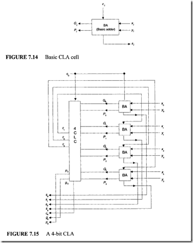
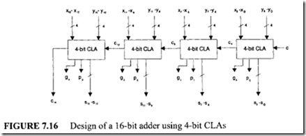
To construct a 4-bit CLA, assume the existence of the basic adder cell shown in Figure 7.14. Using this basic cell and 4-bit CLC, the design of a 4-bit CLA can be completed as shown in Figure 7.15. Using this cell as a building block, a 16-bit adder can be designed as shown in Figure 7.16.
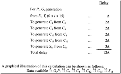
The worst-case add-time of this adder can be calculated as follows:
From this calculation, it is apparent that the new I 6-bit adder is faster than the 16-bit CPA by a factor of 3. In fact, this system can be speeded up further by employing another 4-bit CLC and eliminating the carry propagation between the 4-bit CLA blocks. For this purpose, the gi and Pi outputs generated by the 4-bit CLA are used. This design task is left as an exercise to the reader.
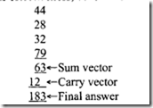
If there is a need to add more than 3 operands, a technique known as "carry-save addition" is used. To see its effectiveness, consider the following example:
In this example, four decimal numbers are added. First, the unit digits are added, producing a sum of3 and a carry digit of2. Similarly, the tens digits are added, producing a sum digit of 6 and a carry digit of 1. Because there is no carry propagation from the unit digit to the tenth digit, these summations can be carried out in parallel to produce a sum vector of 63 and a carry vector of 12. When all operands are exhausted, the sum and the shifted carry vector are added in the conventional manner, which produces the final answer. Note that the carry is propagated only in the last step, which generates the final answer no matter how many operands are added. The concept is also referred to as "addition by deferred carry assimilation."
