Program control instructions , system control instructions and 68000 stack

10.6.1 Program Control Instructions

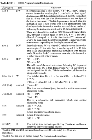
These instructions include branches, jumps, and subroutine calls as listed in Table 10.11.

Consider Bee d. There are 14 branch conditions. This means that the cc in Bee can be replaced by 14 conditions providing 14 instructions: BCC, BCS, BEQ, BGE, BGT, BHI, BLE, BLS, BLT, BMI, BNE, BPL, BVC, and BVS. It should be mentioned that some of these instructions are applicable to both signed and unsigned numbers, some can be used with only signed numbers, and some instructions are applicable to only unsigned numbers.

After signed arithmetic operations, instructions such as BEQ, BNE, BVS, BVC, BMI, and BPL can be used. On the other hand, after unsigned arithmetic operations, instructions such as BCC, BCS, BEQ, and BNE can be used. It should be pointed out that if V = 0, BPL and BGE have the same meaning, Likewise, if V = 0, BMI and BLT perform the same function.

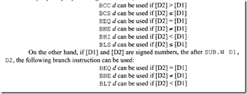
The conditional branch instruction can be used after typical arithmetic instructions such as subtraction to branch to a location if cc is true. For example, consider SUB. W 01, 02. Now if [D1] and [D2] are unsigned numbers, then

image

image

image

Now as a specific example, consider BEQ BEGIN. If current [PC] = 000200 16, and BEGIN=$20 then, after execution of this BEQ, program execution starts at 000220 16 if Z = I; if Z = 0, program execution continues at 000200 16• The instructions BRA and JMP are unconditional jump instructions. BRA uses the relative addressing mode, whereas JMP uses only control addressing mode. For example, consider BRA.B START. If [PC]= 000200 16, and START=$40 then, after execution of this BRA, program execution starts at 000240 16• Now, consider JMP (Al) . If [Al] = 00000220 16, then, after execution of this JMP, program execution starts at 000220 16

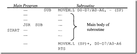
• The instructions BSR and JSR are subroutine call instructions. BSR uses the relative mode, whereas JSR uses the control addressing mode. Consider the following program segment: Assume that the main program uses all registers; the subroutine stores the result in memory.

image

Here, the JSR SUB instruction calls the subroutine SUB. In response to JSR, the 68000 pushes the current PC contents called START onto the stack and loads the starting address SUB of the subroutine into PC. The first MOVEM in the SUB pushes all registers onto the stack and, after the subroutine is executed, the second MOVEM instruction pops all the registers back. Finally, RTS pops the address START from the stack into PC, and program control in returned to the main program. Note that BSR SUB could have been used instead of JSR SUB in the main program. In that case, the 68000 assembler would have considered the SUB with BSR as a displacement rather than as an address with the JSR instruction.

DBcc Dn, d tests the condition codes and the value in a data register. DBcc first checks if cc (NE, EQ, GT, etc.) is satisfied. If cc is satisfied, the next instruction is executed. If cc is not satisfied, the specified data register is decremented by I; if [Dn] = -1, then the next instruction is executed; on the other hand, if Dn ¢ -I, then branch to PC + d is performed. For example, consider DBNE. W DS, BACK with [D5] = 00003002 16, BACK= -4 and [PC] = 00200616• If Z = 1, then [D5] = 00003001 16• Because [D5] ¢ -I, program execution starts at 002002 16• It should be pointed out that there is a false condition in the DBcc instruction and that this instruction is the DBF (some assemblers use DBRA for this). In this case, the condition is always false. This means that, after execution of this instruction, Dn is decremented by I and if [Dn] = -I, then the next instruction is executed. If [Dn] ¢ -I, then branch to PC + d.

image

10.6.2 System Control Instructions

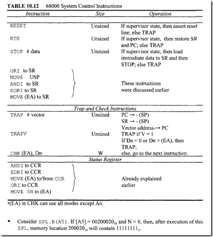
The 68000 system control instructions contain certain privileged instructions including RESET, RTE, STOP and instructions that use or modify SR. Note that the privileged instructions can be executed only in the supervisor mode. The system control instructions are listed in Table 10.12.

  • The RESET instruction when executed in the supervisor mode outputs a low signal on the reset pin of the 68000 in order to initialize the external peripheral chips. The 68000 reset pin is bidirectional. The 68000 can be reset by asserting the reset pin using hardware, whereas the peripheral chips can be reset using the software RESET instruction.
  • MOVE . L A 7 , An or MOVE . L An, A 7 can be used to save, restore, or change the contents of the A 7 in supervisor mode. A 7 must be loaded in supervisor mode because MOVE A 7 is a privileged instruction. For example, A7 can be initialized to $005000 in supervisor mode using MOVEA . L # $ 0 0 0 0 50 0 0 , A 1 MOVE.L Al,A7
  • Consider TRAP #n. There are 16 TRAP instructions with n ranging from 0 to 15.

The hexadecimal vector address is calculated using the equation: Hexadecimal vector address= 80 + 4 x n. The TRAP instruction first pushes the contents of the PC and then the SR onto the stack. The hexadecimal vector address is then loaded into PC. TRAP is basically a software interrupt. The TRAP instruction can be used for service calls to the operating system. For application programs running in the user mode, TRAP can be used to transfer control to a supervisor utility program. RTE at the end of the TRAP routine can be used to return to the application program by placing the saved SR from the stack, thus causing the 68000 to return to the user mode.

There are other traps that occur due to certain arithmetic errors. For example, division by zero automatically traps to location 1416• On the other hand, an overflow condition (i.e., if V = 1) will trap to address 1C16 if the instruction TRAPV is executed.

  • The CHK. W (EA), Dn instruction compares [Dn] with (EA). If [Dn]1ow 16 bits< 0 or if [Dn]1ow 16 bits > (EA), then a trap to location 0018 16 is generated. Also, N is set to 1 if [Dn]10w 16 hits < 0, and N is reset to 0 if [Dn]1ow 16 bits > (EA). (EA) is treated as a 16-bit twos complement integer. Note that program execution continues if [Dn]1ow 16 bits lies between 0 and (EA).

Consider CHK. W (AS), D2. If [D2]1ow 16 bits= 020016, [AS] = 00003000 16, and [003000 16] = 0100 16, then, after execution of this CHK, the 68000 will trap because  [D2] = 020016 is greater than [003000] = 010016

The purpose of the CHK instruction is to provide boundary checking by testing if the content of a data register is in the range from zero to an upper limit. The upper limit used in the instruction can be set equal to the length of the array. Then, every time the array is accessed, the CHK instruction can be executed to make sure that the array bounds have not been violated.

The CHK instruction is usually placed after the computation of an index value to ensure that the index value is not violated. This permits a check of whether or not the address of an array being accessed is within array boundaries when address register indirect with index mode is used to access an array element. For example, the following instruction sequence permits accessing of an array with base address in A2 and array length of 5010 bytes:

imageHere, if the low 16 bits of D2 are less than 0 or greater than 49, the 68000 will trap to location 0018 16• It is assumed that D2 is computed prior to execution of the CHK instruction.

10.6.3 68000 Stack

The 68000 supports stacks with the address register indirect postincrement and predecrement addressing modes. In addition to two system stack pointers (A7 and A7′), all seven address

registers (AO-A6) can be used as user stack pointers by using appropriate addressing modes. Subroutine calls, traps, and interrupts automatically use the system stack pointers: USP (A7) when S = 0 and SSP (A7′ ) when S = l. Subroutine calls push the PC onto the system stack; RTS pops the PC from the stack. Traps and interrupts push both PC and SR onto the system stack; RTE pops PC and SR from the stack.

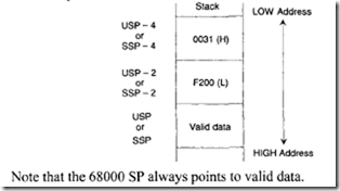
The 68000 accesses the system stack from the top for operations such as subroutine calls or interrupts. This means that stack operations such as subroutine calls or interrupts access the system stack automatically from HIGH to LOW memory. Therefore, the system SP is decremented by 2 for word or 4 for long word after a push and incremented by 2 for word or 4 for long word after a pop. As an example, suppose that a 68000-CALL instruction (JSR or BSR) is executed when PC = $0031F200; then, after execution of the subroutine call, the stack will push the PC as follows:

image

In 68000, stacks can be created by using address register indirect with postincrement or predecrement modes. Typical 68000 memory instructions such as MOVE to/from can be used to access the stack. Also, by using one of the seven address registers (AO-A6) and system stack pointers (A7,A7′), stacks can be filled from either HIGH to LOW memory or vice versa:

1. Filling a stack from HIGH to LOW memory (Top of the stack) is implemented with predecrement mode for push and postincrement mode for pop.

2. Filling a stack from LOW to HIGH (Bottom of the stack) memory is implemented with postincrement for push and predecrement for pop.

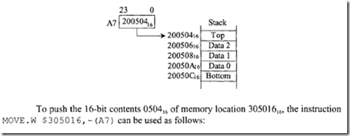
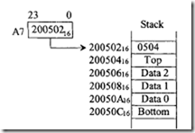
For example, consider the following stack growing from HIGH to LOW memory addresses in which A7 is used as the stack pointer:

image

image

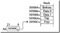
The 16-bit data item 050416 can be popped from the stack into the low 16 bits of D0 by using MOVE. W (A 7) +,D0. Register A 7 will contain 200504 16 after the pop. Note that, in this case, the stack pointer A7 points to valid data. Next, consider the stack growing from LOW to HIGH memory addresses in which the user utilizes A6 as the stack pointer:

image

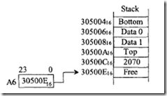
To push the 16-bit contents 2070 16 of the low 16 bits ofD5, the instruction MOVE. w DS, (A 6} + can be used as follows. The 16-bit data item 2070 16 can be popped from the stack into the 16-bit contents of memory location 417024 16 by using MOVE. W – (A6) ,$  417 0 2 4. Note that, in this case, the stack pointer A6 points to the free location above the valid data.
image


Logical instructions , shift and rotate instructions , bit manipulation instructions and binary-coded-decimal instructions

10.6.1 Logical Instructions

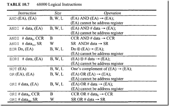
These instructions include logical OR, EOR, AND, and NOT as shown in Table 10.7.

• Consider AND. B # $8 F, DO . If prior to execution of this instruction, [DO.B] = $72, then after execution of AND. B # $ 8 F, D0, the following result is obtained:

imageZ = 0 (Result is nonzero) and N = 0 (Most Significant Bit of the result is 0). C and V are always cleared to 0 after logic operation. The condition codes are similarly affected after execution of other logical instructions such as OR, EOR, and NOT. The AND instruction can be used to perform a masking operation. If the bit value in a particular bit position is desired in a word, the word can be logically ANDed with appropriate data to accomplish this. For example, the bit value at bit 2 of an 8- bit number 0100 IY10 (where unknown bit value ofY is to be determined) can be obtained as follows:

image

If the bit value Y at bit 2 is 1, then the result is nonzero (Flag Z=O); otherwise, the result is zero (Z= 1) . The Z flag can be tested using typical conditional ru MP instructions such as BEQ (Branch if Z= 1) or BNE (Branch if Z=O) to determine

image

whether Y is 0 or I. This is called masking operation. The AND instruction can also be used to determine whether a binary number is ODD or EVEN by checking the Least Significant bit (LSB) of the number (LS8=0 for even and LS8=1 for odd).

  • Consider AND. W Dl, DS. If [Dl.W] = 0001 16 and [D5.W) = FFFF 16, then, after execution of this AND, the low 16 bits of both Dl and D5 will contain 0001 16•
  • Consider ANDI .B #$00, CCR. If[CCR) = 01 16, then, after this ANDI, register CCR will contain 0016
  • Source (EA) in AND and OR can use all modes except An .
  • Destination (EA) in AND or OR or EOR can use all modes except An, relative, and immediate.
  • Destination (EA) in ANDI, 0RI, and EORI can use all modes except An, relative, and immediate.
  • (EA) in NOT can use all modes except An, relative, and immediate .
  • Consider E0R. W # 2, DS . If prior to execution of this instruction, [ DS. W J $2 3 4 2, then after execution of EOR. W # 2, D 5, low 16-bit contents of D5 will be $ 2 3 4 0. All condition codes are affected in the same manner as the AND instruction. The Exclusive-OR instruction can be used to find the ones complement of a binary number by XORing the number with ali i’s as follows:

image

execution of this EOR, register D2.W will contain 0000 16, and Dl will remain unchanged at FFFF 16

• Consider NOT. B 05. If [D5.B] = 02 16,then, after execution of this NOT, the low byte ofD5 will contain FD 16

• Consider OR. B 02, D3 . If prior to execution of this instruction, [D2.B] = A2 16 and lD3.B] = 5D16, then after exection of OR. B 02, 03, the contents of D3.B are FFH. All flags are affected similar to the AND instruction. The OR instruction can typically be used to insert a 1 in a particular bit position of a binary number without changing the values of the other bits. For example, a 1 can be inserted using the OR instruction at bit number 3 of the 8-bit binary number 0 1 1 1 0 0 1 1 without changing the values of the other bits as follows:

image

  • Consider ORI #$1002, SR. If [SR] = 111D16, then after execution of this ORI, register SR will contain lllF16• Note that this is a privileged instruction because the high byte of SR containing the control bits is changed and therefore, can be executed only in the supervisor mode.

10.6.2 Shift and Rotate Instructions

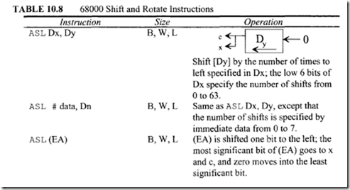
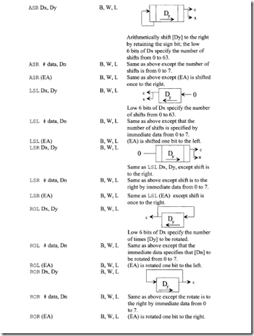
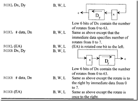
The 68000 shift and rotate instruction are listed in Table I0.8.

• All the instructions in Table 10.8 affect Nand Z flags according to the result. Vis reset to zero except for ASL.

• Note that in the 68000 there is no true arithmetic shift left instruction. In true arithmetic shifts, the sign bit of the number being shifted is retained. In the 68000, the instruction ASL does not retain the sign bit, whereas the instruction ASR retains the sign bit after performing the arithmetic shift operation.

image

image

image

• (EA) in ASL, ASR, LSL, LSR, ROL, ROR, ROXL, and ROXR can use all modes except Dn, An, relative, and immediate.

• Consider ASL. W Dl, 05. If [D1]1ow 16 bits = 0002 16 and [D5]1ow 16 bits = 9FF0 16, then, after this ASL instruction, [D5]10w l6bits = 7FC016, C = 0, and X= 0. Note that the sign of the contents of D5 is changed from 1 to 0 and, therefore, the overflow is set. The sign bit of D5 is changed after shifting [D5] twice. For ASL, the overflow flag is set to one if the sign bit changes during or after shifting. The contents of D5 are not updated after each shift. The ASL instruction can be used to multiply a signed number by 2" by shifting the number n times to the left; the result is correct if V = 0 while the result is incorrect if V = 1. Since execution time of the multiplication instruction is longer, multiplication by shifting may be more efficient when multiplication of a signed number by 2" is desired.

• ASR retains the sign bit. For example, consider ASR. W #2, Dl. If[D1.W] = FFE2 16, then, after this ASR, the low 16 bits of [D1] = FFF8 16, C = 1, and X = 1. Note that the sign bit is retained.

• ASL (EA) or ASR (EA) shifts (EA) 1 bit to left or right, respectively. For example, consider ASL. W (AO). If [AO] = 00002000 16 and [00200016] = 9001 16, then, after execution of this ASL, [00200016] = 2002 16, X= 1, and C = 1. On the other hand, after ASR. w (AO), memory location 002000 16 will contain C80016, C = 1, and X= I.

• The LSL and ASL instructions are the same in the 68000 except that with the ASL, V is set to 1 if the sign of the result is changed from the sign of the original value during or after shifting. This will allow one to multiply a signed number by 2" by shifting the number n times to left; the result is correct if V = 0 while the result is incorrect if V = 1. Since execution time of the multiplication instruction is longer, multiplication by shifting may be more efficient when multiplication of a signed number by 2" is desired.

image

  • (EA) in the above instructions can use all modes except An, relative, and immediate.
  • If (EA) is memory location then data size is byte: if (EA) is Dn then data size is long word.
  • Consider LSR. W # 3, 01. If [Dl.W] = 800016,then after this LSR, (Dl.W] = 100016, X= 0, and C = 0.
  • Consider ROL. B #2, 02. If [D2.B] = B1 16 and C = 1, then, after this ROL, the low byte of [D2] = C616 and C = 0. On the other hand, with [D2.B] = B 116 and C = I, consider ROR. B # 2, 02. After this ROR, low byte of register D2 will contain 6C 16 and C =0.
  • Consider ROXL. W 02, 01. If [D2.W] = 000316, [Dl.W] = F201 16, C = 0, and X= I then after execution of this ROXL, [D1.W] = 900F16, C = I, and X = 1.

10.6.3 Bit Manipulation Instructions

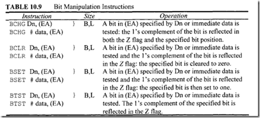
The 68000 has four bit manipulation instructions, and these are listed in Table 10.9.

  • In all of the instructions in Table 10.9, the ones complement of the specified bit is reflected in the Z flag. The specified bit is ones complemented, cleared to 0, set to I, or unchanged by BCHG, BCLR, BSET, or BTST, respectively. In all the instructions in Table 10.9, if(EA) is Dn, then the length of Dn is 32 bits; otherwise, the length ofthe destination is one byte memory.
  • Consider BCHG. B #2, $0 03 0 0 0. If [003000 16] = 05 16, then, after execution of this BCHG, Z = 0 and [00300016] = 01 16•
  • Consider BCLR. L # 3, 01. If [Dl] = F210E128 16, then after execution of this BCLR, register D1 will contain F210E120 16 and Z = 0.
  • Consider BSET. B #0, (Al). If[AI]= 00003000 16 and [00300016] = 0016, then, after execution of this BSET, memory location 003000 16 will contain 01 16 and Z = 1.
  • Consider BTST. B #2, $0 02 0 0 0. If [002000 16] = 02 16, then, after execution of this BTST, Z = 1, and [00200016] = 02 16; no other flags are affected.

10.6.4 Binary-Coded-Decimal Instructions

The 68000 instruction set contains three BCD instructions, namely, ABCD for adding, SBCO for subtracting, and NBCO for negating. They operate on packed BCD byte(s) and provide the result containing one packed BCD byte. These instructions always include the

image

extend (X) bit in the operation. The BCD instructions are listed in Table 10.10.

  • Consider ABCO.B D1, D2. If[Dl.B] = 25 10, [D2.B] = 1510, and X= 0, then, after execution of this ABCO instruction, [D2.B] = 4010, X= 0, and Z = 0.
  • Consider SBCO. B – (A2) , – (A3). If [A2] = 00002004 16, [A3] = 00003003 16, [002003 16] = 0510, [003002 16] = 0610, and X= 1, then after execution of this SBCD instruction, [00300216] = 0010, X = 0, and Z = 1.
  • Consider NBCO. B (Al). If[A1] = [0000300016], [00300016] =0510, and X= 1, then, after execution of this NBCO instruction, [00300016] = -610

Note that packed BCD subtraction used in the instructions SBCO and NBCO can be obtained

by using the concepts discussed in Chapter 2 (Section 2.5.2).


68000 Delay Routine

10.7 68000 Delay Routine

Typical 68000 software delay l00ps can be written using MOVE and DBF instructions. For example, the following instruction sequence can be used for a delay l00p of 2 millisecond:

image

Note that DBF.W in the above decrements D0 .W by one, and if DO.W "’ -1 branches to DELAY; ifDO.W = -1, the 68000 executes the next instruction. Since DBF.W checks for DO.W for -1, the value of "count" must be one less than the required l00p count. The initial l00p counter value of "count" can be calculated using the cycles (Appendix D)

required to execute the following 68000 instructions:

image

DBF.W requires IO cycles when the 68000 branches if the content of D0.W is not equal to -1after autodecrementing D0.W by I. However, the 68000 goes to the next instruction and does not branch when [D0.W] = -1 after autodecrementing DO.W by 1, and this requires 14 cycles. This means that the DELAY l00p will require 10 cycles for "count" times, and the last iteration will take I4 cycles.

image

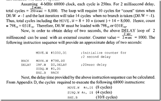
As before, assuming 4-MHz 68000 clock, each cycle is 250ns. Total time from the above instruction sequence for two-second delay= Execution time for MOVE.W + 1000 * (2 msec delay)+ 1000 *(Execution time for SUBQ.W) + 999* (Execution time for BNE.B for Z = 0 when Dl ..- 0) +(Execution time for BNE.B for Z = 1 when D1 = 0 for last iteration) = 8 * 250ns + I 000 * 2msec + 1000 * 4 * 250ns + 999 * 10 * 250ns + 8 * 250ns = 2.0035 seconds which is approximately 2 seconds discarding the execution times of MOVE.W, SUBQ.W, and BNE.B.


Example on 68000 programming part 1

Example 10.1

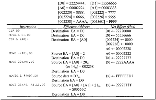
Determine the effect of each of the following 68000 instructions:

  • CLR D0
  • MOVE. L D1, D0
  • CLR.L (A0) +
  • MOVE -(A0), D0
  • MOVE 20 (A0 ), D0
  • MOVEQ.L #$D7, D0
  • MOVE 21 (A0, Al.L), D0

Assume the following initial configuration before each instruction is executed; also assume all numbers in hex:

image

Example 10.2

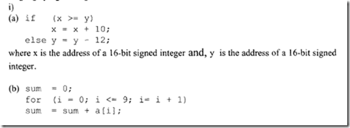
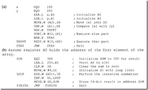
Write a 68000 assembly language program that implements each of the following C language program segments:

imagewhere sum is the address of the 16-bit result of addition.

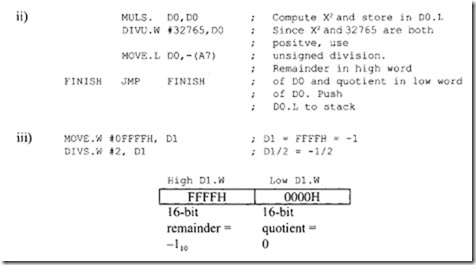
ii) Write a 68000 assembly language program to find (X2) I (3276510) where X is a 16-bit signed number stored in D0.W. Store the 32-bit result (quotient and remainder) onto the user stack.

iii) What are the remainder, quotient, and register containing them after execution of the following 68000 instruction sequence?

image

image

Note that, in the above condition Fin DBF is always false. Hence, the program exits from the LOOP when D I= -1. Therefore, the addition process is performed 10 times.

image

Example 10.3

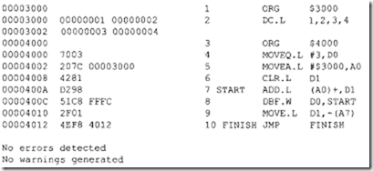
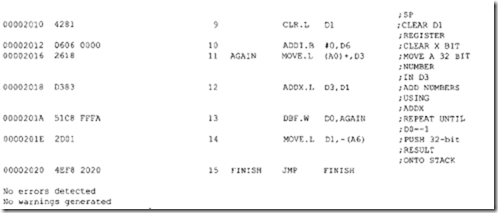
Write a 68000 assembly program at address $002000 to clear l 0010 consecutive bytes (from low to high addresses) to zero starting at location $003000.

Solution

image

No warnings generated

Note that the 68000 has no HALT instruction .. Therefore, the unconditional jump to the same location such as FINISH JMP FINISH is normally used at the end of the program. Because DBF is a word instruction and considers D0’s low 16-bit word as the l00p count, one should be careful about initializing D0 using MOVEQ. L #d8, Dn since this instruction sign extends low byte of Dn to 32 bits.

Example 10.4

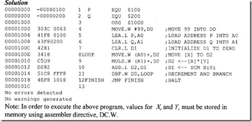
Write a 68000 assembly language program at address $001000 to compute image where

X1. and Yi are signed 16-bit numbers and N = 100. Store the 32-bit result in D 1. Assume that the starting addresses of X. and Yj are 10016 and 20016 respectively.

image

Example 10.5

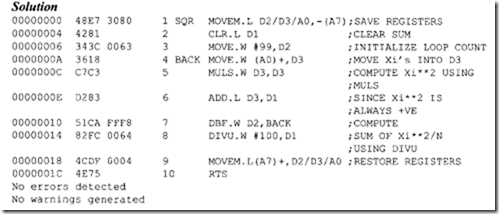
Write a 68000 subroutine to compute Y = image. Assume the X.’s are 16-bit signed integers and N = 100. The numbers are stored in consecutive locations. Assume A0 points to the X/s and A7 is already initialized in the main program. Store 32-bit result in D1 (16-bit remainder in high word of Dl and 16-bit quotient in the low word of Dl). Assume user mode.

image

In the above program, DIVU is used for computing LXi2/N since both SUM (Xi**2) and N=I00 are unsigned (positive). Note that in order to execute the above program, values for must be stored in memory using assembler directive, DC.W.

Example 10.6

Write a 68000 assembly language program at address 0 to move a block of 16-bit data of length I 0010 from the source block starting at location 002000 16 to the destination block starting at location 003000 16 from low to high addresses.

Solution

image

Note: Typical assemblers assemble a program starting at address 0 if assembler directive ORG is not used at the beginning of the program.

Example 10.7

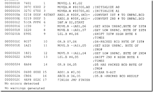
Write a 68000 assembly language program at address 0 to add two words, each containing two ASCII digits. The first word is stored in two consecutive locations (from LOW to HIGH) with the low byte pointed to by A0 at address 000300 16, and the second word is stored in two consecutive locations (from LOW to HIGH) with the low byte pointed to by AI at 000700 16• Store the packed BCD result in D5.

Solution

image


Example on 68000 programming

Example 10.8

Write a 68000 assembly language program that will perform : 5 x X+ 6 x Y + [Y/8] [ D l.L] where X is an unsigned 8-bit number stored in the lowest byte of D0 and Y is a 16-bit signed number stored in the upper 16 bits of D I.Neglect the remainder of Y/8.

Solution

imageExample 10.9

Write a 68000 assembly language program to convert temperature from Fahrenheit to Celsius using the following equation: C = [(F- 32)/9] x 5 ; assume that the low byte of D0 contains the temperature in Fahrenheit. The temperature can be positive or negative. Store result in D0.

Solution

image

Example 10.10

Write a 68000 assembly language program at address $4000 to add four 32-bit numbers stored in consecutive locations starting at address $3000. Store the 32-bit result onto the user stack. Assume that no carry is generated due to addition of two consecutive 32-bit numbers and A7 is already initialized.

Solution

image

Example 10.11

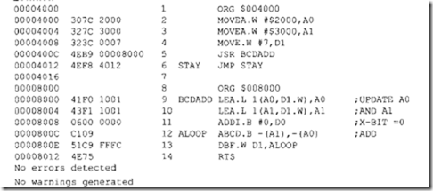
Write a subroutine in 68000 assembly language to implement the C language assignment statement: p = p + q; where addresses p and q hold two 16-digit (64-bit) packed BCD numbers (Nl and N2). The main program will initialize addresses p and q to $002000 and $003000 respectively. Address $002007 will hold the lowest byte ofNl with the highest byte at address $002000 while Address $003007 will contain the lowest byte of N2 with the highest byte at address $003000. Also, write the main program at address $004000 which will perform all initializations including address p (pointer AO to $002000), address q (pointer AI to $003000), l00p count (D1 to 7), and then call the subroutine at $008000 and stop. The subroutine will accomplish the task with the initialized values of AO, A I, and D1 in the main program. Use ABCD.B for BCD addition with predecrement mode. Assume supervisor mode. Note that the 68000 supervisor stack pointer is initialized upon hardware reset.

Solution

image

Examule 10.12

Write a 68000 assembly program to multiply an 8-bit signed number in the low byte ofDI by a 16-bit signed number in the high word ofD5. Store the result in D3.

Solution

imageExamule 10.13

Write a 68000 assembly language program at address $2000 to add ten 32-bit numbers stored in consecutive locations starting at address $502040. Initialize A6 to $00200504 and use the low 24 bits of A6 as the stack pointer to push the 32-bit result. Use only ADDX instruction for adding two 32-bit numbers each time through the l00p. Assume that no carry is generated due to the addition of two consecutive 32-bit numbers; this will provide the 32-bit result. This example illustrates use of the 68000 ADDX instruction.

Solution


image

image

Note that ADDX adds the contents of two data registers or the contents of two memory locations using predecrement modes.

Example 10.14

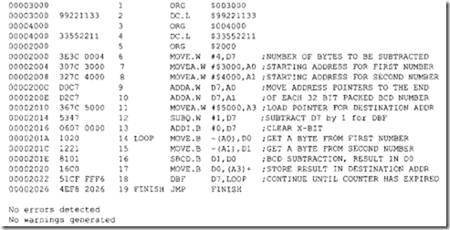
Write a 68000 assembly language program at address $2000 to subtract two 32-bit packed BCD numbers. The BCD number 1 is stored at the locations starting from $003000 through $003003, with the least significant byte at $003003 and the most significant byte at $003000. Similarly, the BCD number 2 is stored at the locations starting from $004000 through $004003, with the least significant byte at $004003 and the most significant byte at $004000. The BCD number 2 is to be subtracted from BCD number 1. Store the packed BCD result at addresses $005000 (Lowest byte of the result) through $005003 (Highest byte of the result). In the program, first initialize l00p counter D7 to 4, source pointer AO to $003000, source pointer A I to $004000, destination pointer A3 to $005000, and then write the program to accomplish the above using these initialized values.

Solution

image

Note that SBCD subtracts the contents of two data registers or the contents of two memory locations using predecrement modes.

Example 10.15

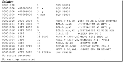
Write a 68000 assembly program at address $1000 which is equivalent to the following C language segment:

image

Assume that the arrays, x[i] and y[i] contain unsigned 16-bit numbers already stored in memory starting at addresses $3000 and $4000 respectively. Store the 32-bit result at address $5000.

image


Functional categories of 68000 addressing modes , 68000 instruction set , data movement instructions , exg and swap instructions , lea and pea instructions , link and unlk instructions , arithmetic instructions , addition and subtraction instructions , multiplication and division instructions , compare, clear, and negate instructions , test instruction , test and set instruction .

10.5 Functional Categories Of 68000 Addressing Modes

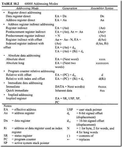
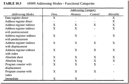
All of the 68000 addressing modes in Table 10.2 can be further divided into four functional categories as shown in Table 10.3.

Data Addressing Mode. An addressing mode is said to be a data addressing mode if it references data objects. For example, all 68000 addressing modes except the address register direct mode fall into this category.

Memory Addressing Mode. An addressing mode capable of accessing a data item stored in memory is classified as a memory addressing mode. For example, the data and address register direct addressing modes cannot satisfy this definition.

Control Addressing Mode. This refers to an addressing mode that has the ability to access a data item stored in memory without the need to specify its size. For example, all 68000 addressing modes except the following are classified as control addressing

imagemodes: data register direct, address register direct, address register indirect with postincrement, address register indirect with predecrement, and immediate.

Alterable Addressing Mode. If the effective address of an addressing mode is written into, then that mode is an alterable addressing mode. For example, the immediate and the program counter relative addressing modes will not satisfy this definition.

10.6 68000 Instruction Set

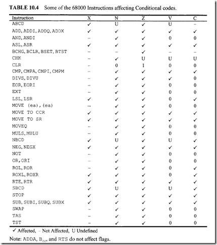
The 68000 instruction set contains 56 basic instructions. Table 10.4 lists some of the instructions affecting the condition codes. Appendices D and G provide the 68000 instruction execution times and the instruction set (alphabetical order), respectively.

The 68000 instructions can be classified into eight groups as follows:

image

• (EA) in LEA (EA), An can use all addressing modes except Dn, An, (An)+,- (An), and immediate.

• Destination (EA) in MOVE (EA), (EA) can use all modes except An, relative, and immediate.

• Source (EA) in MOVE (EA), (EA) can use all modes .

• Destination (EA) in MOVEM reg list, (EA) can use all modes except, An, (An)+, relative, and immediate.

• Source (EA) in MOVEM (EA), reg list can use all modes except Dn, An,- (An), and immediate.

• (EA) in PEA (EA) can use all modes except, An, (An)+, -(An), and immediate .

1. Data movement instructions

2. Arithmetic instructions

3. Logical instructions

4. Shift and rotate instructions

5. Bit manipulation instructions

6. Binary-coded decimal instructions

7. Program control instructions

8. System control instructions

10.6.1 Data Movement Instructions

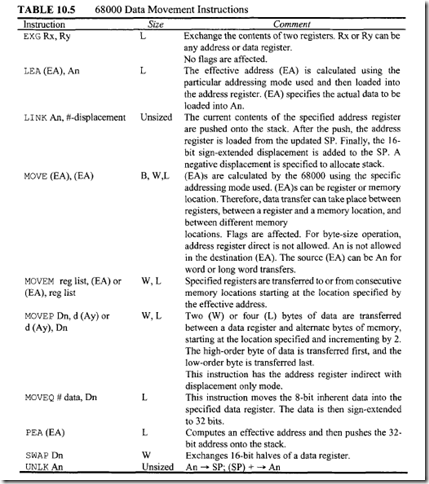
These instructions allow data transfers from register to register, register to memory, memory to register, and memory to memory. In addition, there are also special data movement instructions such as MOVEM (move multiple registers). Typically, byte, word, or long word data can be transferred. A list of the 68000 data movement instructions is given in Table

10.5. Let us now explain the data movement instructions.

MOVE Instructions

The format for the basic MOVE instruction is MOVE. S (EA), (EA), where S = L, W, or B. (EA) can be a register or memory location, depending on the addressing mode used. Consider MOVE. B 03, 01, which uses the data register direct mode for both the source and destination. If [D3.B] = 0516 and [D l.B] = 01 16, then, after execution of this MOVE instruction, [Dl.B] = 0516 and [D3.B] = 0516

There are several variations of the MOVE instruction. For example MOVE. W CCR, (EA) moves the contents of the low-order byte of SR (i.e., CCR) to the low-order byte of the destination operand; the upper byte of SR is considered to be zero. The source operand is a word. Similarly, MOVE. W (EA), CCR moves an 8-bit immediate number, or low-order 8-bit data, from a memory location or register into the condition code register; the upper byte is ignored. The source operand is a word. Data can also be transferred between (EA) and SR r USP (A7) using the following privileged instructions:

imageMOVEA. W or. L (EA), An can be used to load an address into an address register. Word-size source operands are sign-extended to 32 bits. Note that (EA) is obtained by using an addressing mode. As an example, MOVEA. W # $ 2 0 0 0, AS moves the 16-bit word 2000 16 into the low 16 bits of AS and then sign-extends 2000 16 to the 32-bit number 00002000 16• Note that sign extension means extending bit 15 of 2000 16 from bit 16 through bit 31. As mentioned before, sign extension is required when an arithmetic operation between two signed binary numbers of different sizes is performed. The (EA) in MOVEA can use all addressing modes.

The MOVEM instruction can be used to push or pop multiple registers to or from the stack. For example, MOVEM.L 00-07 /AO-A6,- (SP) saves the contents of all eight data registers and seven address registers in the stack. This instruction stores address registers in the order A6-AO first, followed by data registers in the order D7-DO, regardless of the order in the register list. MOVEM .L ( sP) +, DO-D7 I A 0-A 6 restores the contents of the registers in the order D0-D7, A0-A6, regardless of the order in the register list.

The MOVEM instruction can also be used to save a set of registers in memory. In addition to the preceding predecrement and postincrement modes for the effective address, the MOVEM instruction allows all the control modes. If the effective address is in one of the control modes, such as absolute short, then the registers are transferred starting at the specified address and up through higher addresses. The order of transfer is from DO to D7 and then from AO to A6. For example, MOVEM. W A5/0l/03/Al-A3, $2000 transfers the low 16-bit contents of Dl, D3, AI, A2, A3, and A5 to locations $2000, $2002, $2004, $2006, $2008, and $200A, respectively.

The MOVEQ. L # $d8, Dn instruction moves the immediate 8-bit data into the low byte of Dn. The 8-bit data is then sign-extended to 32 bits. This is a one-word instruction. For example, MOVEQ. L # $8 F, 05 moves $FFFFFF8F into D5.

To transfer data between the 68000 data registers and 6800 (8-bit) peripherals, the MOVEP instruction can be used. This instruction transfers 2 or 4 bytes of data between a data register and alternate byte locations in memory, starting at the location specified and incrementing by 2. Register indirect with displacement is the only addressing mode used with this instruction. If the address is even, all transfers are made on the high-order half of the data bus; if the address is odd, all transfers are made on the low-order half of the data bus. The high-order byte to/from the register is transferred first, and the low-order byte is transferred last. For example, consider MOVEP. L $0020 (A2), 01. If [A2] = $00002000, [00202016] = 02, [00202216] = 05, [00202416] = 01, and [00202616] = 04, then, after execution of this MOVEP instruction, Dl will contain 02050104 16

EXG and SWAP Instructions

The EXG. L Rx, Ry instruction exchanges the 32-bit contents of Rx with that of Ry. The exchange is between two data registers, two address registers, or an address register and a data register. The EXG instruction exchanges only 32-bit-long words. The data size (L) does not have to be specified after the EXG instruction because this instruction has only one data size (L) and it is assumed that the default is this single data size. No flags are affected. The SWAP. W Dn instruction, on the other hand, exchanges the low 16 bits of Dn with the high 16 bits of Dn. All condition codes are affected.

LEA and PEA Instructions

The LEA. L (EA), An instruction moves an effective address (EA) into the specified address register. The (EA) can be calculated based on the addressing mode of the source. For example, LEA $0 0 2 56 0 2 2, A5 moves $002S6022 into AS. This instruction is equivalent to MOVEA. L # $0 02 5 6022, A5. Note that $002S6022 is contained in PC. It should be pointed out that the LEA instruction is very useful when address calculation is desired during program execution. The (EA) in LEA specifies the actual data to be loaded into An, whereas the (EA) in MOVEA specifies the address of actual data. For example, consider LEA $0 4 (A5, D2 .W) , A3. If [AS] = 00002000 16 and [D2] = 0028 16, then the LEA instruction moves 0000202C 16 into A3. On the other hand, MOVEA $04 (A5, 02. W) , A3 moves the contents of 00202C 16 into A3. Therefore, it is obvious that if address calculation is required, the instruction LEA is very useful.
The PEA.L (EA) computes an effective address and then pushes it on to the Supervisor stack (S=l) or User stack (S=O). This instruction can be used when the 16- bit address in absolute short mode is required to be pushed onto the stack. For example, consider PEA.L $9000 in the user mode. If [A7]=$00003006, then $9000 is sign-extended to 32 bits ($FFFF9000). The low-order 16 bits ($9000) are pushed at $003004, and the high order 16 bits ($FFFF) are pushed at $003002.

image

LINK and UNLK Instructions

Before calling a subroutine, the main program quite often transfers the values of certain parameters to the subroutine. It is convenient to save these variables onto the stack before calling the subroutine. These variables can then be read from the stack and used by the subroutine for computations. The 68000 LINK and UNLK instructions are used for this purpose. In addition, the 68000 LINK instruction allows one to reserve temporary storage for the local variables of a subroutine. This storage can be accessed as needed by the subroutine and can be released using UNLK before returning to the main program. The LINK instruction is usually used at the beginning of a subroutine to allocate stack space for storing local variables and parameters for nested subroutine calls. The UNLK instruction is usually used at the end of a subroutine before the RETURN instruction to release the local area and restore the stack pointer contents so that it points to the return address.

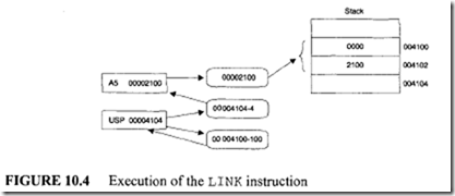
The LINK An, #- displacement instruction causes the current contents of the specified An to be pushed onto the system stack. The updated SP contents are then loaded into An. Finally, a sign-extended twos complement displacement value is added to the SP. No flags are affected. For example, consider LINK A5, #-$10 0. If [AS] = 00002100 16 and [USP] = 00004104 16,then after execution of the LINK instruction, the situation shown in Figure 10.4 occurs. This means that after the LINK instruction, [AS]= $00002100 is pushed onto the stack and the [updated USP] = $004100 is loaded into AS. USP is then loaded with $004000 and therefore 10016 locations are allocated to the subroutine at the beginning of which this particular LINK instruction can be used. Note that AS cannot be used in the subroutine.

The UNLK instruction at the end of this subroutine before the RETURN instruction releases the 10016 locations and restores the contents of AS and USP to those prior to using the LINK instruction. For example, UNLK A5 will load [AS] = $00004100 into USP and the two stack words $00002100 into AS. USP is then incremented by 4 to contain $00004104. Therefore, the contents of AS and USP prior to using the LINK instruction are restored.

In this example, after execution of the LINK, addresses $0003FF and below can be used as the system stack. One hundred (Hex) locations starting at $004000 and above can be reserved for storing the local variables of the subroutine. These variables can then be accessed with an address register such as AS as a base pointer using the address register indirect with displacement mode. MOVE. W d (A5) , Dl for read and MOVE. W Dl, d (A5) for write are typical examples.

image

image

The LINK instruction is used in this case to allocate 50 bytes for local variables. At the end of the subroutine, UNLK A2 is used before RTS to restore the original values of the registers and the stack. RTS returns program execution in the main program.

10.6.2 Arithmetic Instructions

These instructions allow:

  • 8-, 16-, or 32-bit additions and subtractions.
  • 16-bit by 16-bit multiplication (both signed and unsigned) and 32-bit by 16-bit division (both signed and unsigned)
  • Compare, clear, and negate instructions.
  • Extended arithmetic instruction for performing multiprecision arithmetic.
  • Test (TST) instruction for comparing the operand with zero.
  • Test and set (TAS) instruction, which can be used for synchronization in a multiprocessor system.

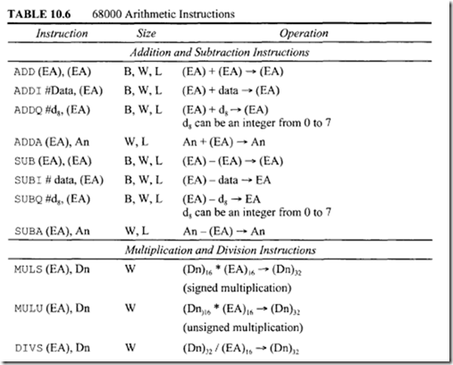
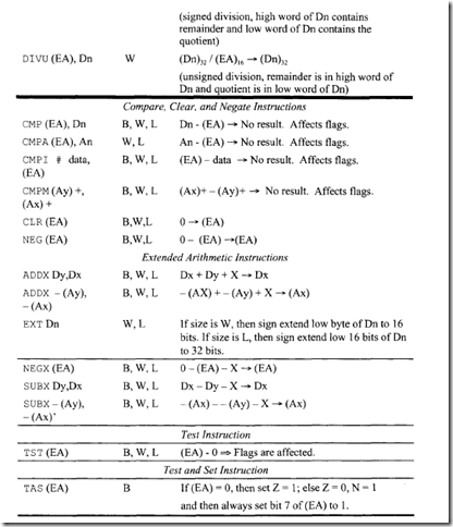
The 68000 arithmetic instructions are summarized in Table 10.6. Let us now explain the arithmetic instructions.

image

image

NOTE: If source (EA) in the ADDA or SUBA instruction is an address register, the operand length is WORD or LONG WORD.

(EA) in any instruction is calculated using the addressing mode used.

All instructions except ADDA and SUBA affect condition codes.

• Source (EA) in the above ADD, ADDA, SUB, and SUBA can use all modes. Destination (EA) in the above ADD and SUB instructions can use all modes except An. relative, and immediate.

• Destination (EA) in ADDI and SUBI can use all modes except An. relative, and immediate.

• Destination (EA) in ADDQ and SUBQ can use all modes except relative and immediate.

• (EA) in all multiplication and division instructions can use all modes except An.

• Source (EA) in CMP and CMPA instructions can use all modes.

• Destination (EA) in CMPI can use all modes except An, relative, and immediate.

• (EA) in CLR and NEG can use all modes except An, relative, and immediate.

• (EA) in NEGX can use all modes except An, relative and immediate.

• (EA) in TST can use all modes except An, relative, and immediate.

• (EA) in TAS can use all modes except An, relative, and immediate.

Addition and Subtraction Instructions

• Consider ADD. W $122 0 00, D0. If[122000 16] = 0012 16 and [DO]= 000216, then, after execution of this ADD, the low 16 bits of DO will contain 0014 16• C = 0 (No Carry), X = 0 (Same as C), V=O (No Overflow since previous Carry and the final Carry are the same), N = 0 (Most Significant Bit of the result is 0), Z = 0 (Nonzero result).

• The ADDI instruction can be used to add immediate data to a register or memory location. The immediate data follows the instruction word. For example, consider ADDI. W #$ 0 012, $1002 00. If [10020016] = 0002 16, then, after execution of this ADDI, memory location 10020016 will contain 001416•

• ADDQ adds a number from 0 to 7 to the register or memory location in the destination operand. This instruction occupies 16 bits, and the immediate data 0 to 7 is specified by 3 bits in the instruction word. For example, consider ADDQ. B #2, Dl. If [D1]1ow byte= 20 16, then, after execution of this ADDQ, the low byte of register Dl will contain 2216·

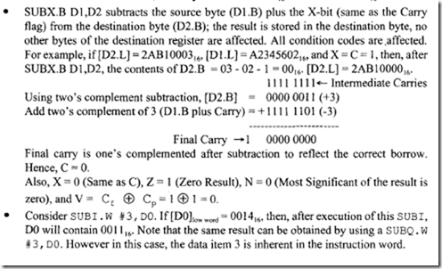
• All subtraction instructions subtract the source from the destination. For example, consider SUB. W D2, $1222 00. lf[D2]1owworct = 0003 16 and [12220016] = 0007 16, then, after execution of this SUB, memory location 12220016 will contain 000416•

imageMultiplication and Division Instructions

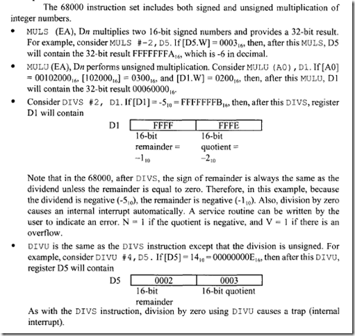
The 68000 instruction set includes both signed and unsigned multiplication of integer numbers.

imageCompare, Clear, and Negate Instructions

• The Compare (CMP) instruction subtracts source from destination providing no result of subtraction; all condition codes are affected based on the result. Note that the SUBTRACT instruction provides the result and also affects the Condition Codes. Consider CMP. B D3, DO . If prior to execution of the instruction, [DO.B] = $40 and [D3.B] = $30 then after execution of CMP. B D3, DO, the condition codes are as follows: C = 0, X= 0, Z = 0, N = 0, and V = 0. Suppose it is desired to find the number of matches for an 8-bit number in a 68000 register such as D5.B in a data array (stored from low to high memory) of 50 bytes in memory pointed to by AO. The following instruction sequence with CMP. B (AD)+, D5 rather than SUB. B (AD) +, D5 can be used:

image

In the above, if SUB. B (AO) +,OS were used instead of CMP. B (AO) +, DS, the number to be matched needs to be loaded after each subtraction because the contents of D5.B would have been lost after each SUB. Since we are only interested in the match rather than the result, CMP. B (AO) +, DS instead of SUB. B (AD)+, DS should be used in the above.

• The 68000 instruction set includes a memory to memory COMPARE instruction. Forexample, CMPM.W (AD)+, (Al)+.If[A0]=00100000 16,[A1]=00200000 16, [ 100000 16] = 0005 1"’ and [20000016] = 0006 16,then, after this CMPM instruction, N = 0, C = 0, X= 0, V = 0, Z = 0, [AO] = 00100002 16,and [AI]= 00200002 16

• CLR. L DS clears all32 bits ofD5 to zero.

• Consider NEG. W (AD). If[AO] = 00200000 16 and [200000] = 510, then after this NEG instruction, the low I6 bits of location 200000 16 will contain FFFB 16

Extended Arithmetic Instructions

• The ADDX and SUBX instruction can be used in performing multiprecision arithmetic because there are no ADDC (add with carry) or SUBC (subtract with borrow) instructions. For example, in order to perform a 64-bit addition, the following two instructions can be used:

image

Note that in this example, DIDO contain one 64-bit number and D6D5 contain the other 64-bit number. The 64-bit result is stored in D6D5.

• Consider EXT. W D2. If[D2]1owbyte = F3 16, then, after the EXT, [D2]1owword = FFF3 16•

• An example of sign extension is that, to multiply a signed 8-bit number by a signed 16-bit number, one must first sign-extend the signed 8-bit into a signed 16-bit number and then the instruction IMUL can be used for 16 x I6 signed multiplication. For unsigned multiplication of a 16-bit number by an 8-bit number, the 8-bit number must be zero extended to I6 bits using logical instruction such as AND before using the MUL instruction.

Test Instruction

Consider TST. W (AO). If [AO] = 00300000 16 and [30000016] = FFFF 16, then, after the TST. W (AD), the operation FFFF 16 – 0000 16 is performed internally by the 68000, Z is cleared to 0, and N is set to 1. The V and C flags are always cleared to 0.

Test and Set Instruction

TAS. B (EA) is usually used to synchronize two processors in multiprocessor data transfers. For example, consider the two 68000-based microcomputers with shared RAM as shown in Figure 10.5.

image

Suppose that it is desired to transfer the low byte of D0 from processor 1 to the low byte of D2 in processor 2. A memory location, namely, TRDATA, can be used to accomplish this. First, processor 1 can execute the TAS instruction to test the byte in the shared RAM with address TEST for zero value. If it is, processor 1 can be programmed to move the low byte of D0 into location TRDATA in the shared RAM. Processor 2 can then execute an instruction sequence to move the contents of TRDATA from the shared RAM into the low byte ofD2. The following instruction sequence will accomplish this:

image

Note that in these instruction sequences, TAS. B TEST checks the byte addressed by TEST for zero. If [TEST] = 0, then Z is set to 1; otherwise, Z = 0 and N = 1. After this, bit 7 of [TEST] is set to 1. Note that a zero value of [TEST] indicates that the shared RAM is free for use, and the Z bit indicates this after the TAS is executed. In each of the instruction sequences, after a data transfer using the MOVE instruction, [TEST] is cleared to zero so that the shared RAM is free for use by the other processor. To avoid testing the TEST byte simultaneously by two processors, the TAS is executed in a read-modify-write cycle. This means that once the operand is addressed by the 68000 executing the TAS, the system bus is not available to the other 68000 until the TAS is completed.


Motorola mc68000 : introduction , 68000 registers , 68000 memory addressing , 68000 addressing modes , register direct addressing , address register indirect addressing , absolute addressing , program counter relative addressing , immediate data addressing and implied addressing .

MOTOROLA MC68000

This chapter describes the basic features of Motorola’s MC68000 (16-bit microprocessor). The addressing modes, instruction set, I/O, and system design concepts of the MC68000 are covered in detail.

Motorola’s original MC68000 was designed using HMOS technology. Motorola’s MC68000 is replaced it by a lower power MC68HC000, which is designed using HCMOS technology. The MC68HC000 is equivalent to the MC68000 in all aspects except that the MC68HC000 is designed using HCMOS whereas the MC68000 was designed using HMOS technology. This means that unlike the MC68000, the unused inputs of the MC68HC000 should not be kept floating, they should be connected to +5 V, ground, or outputs of other chips as appropriate. Also, note that an HCMOS output can drive l 0 LSTTL inputs. However, an LSTTL output is not guaranteed to provide HCMOS input voltage. Hence, the HCT gates may be required when driving HC inputs. The MC 68HC000 has the same registers, addressing modes, instruction set, pins and signals, and I/O capabilities as the MC68000. The term "MC68000" will be used interchangeably with the term "MC68HC000" throughout this chapter.

The MC68HC000, implemented in HCMOS, is applicable to designs for which the following considerations are relevant:

  • The MC68HC000 completely satisfies the input/output drive requirements ofHCMOS logic devices.
  • The· MC68HC000 provides an order of magnitude reduction in power dissipation when compared to the HMOS MC68000.
  • The minimum operating frequency of the MC68HC000 is 4 MHz.

Although the MC68HC000 is implemented with input protection diodes, care should be exercised to ensure that the maximum input voltage specification (-0.3 V to +6.5 V) is not exceeded.

10.1 Introduction

The MC68000 is Motorola’s first 16-bit microprocessor. Its address and data registers are all 32 bits wide, and its ALU is 16 bits wide. The 68000 requires a single 5-V supply. The processor can be operated from a maximum internal clock frequency of 25 MHz. The 68000 is available in several frequencies, including 4, 6, 8, 10, 12.5, 16.67, and 25 MHz. The 68000 does not have on-chip clock circuitly and therefore, requires an external crystal oscillator or clock generator/driver circuit to generate the clock.

The 68000 has several different versions, which include the 68008, 68010, and 68012. The 68000 and 68010 are packaged either in a 64-pin DIP (dual in-line package)

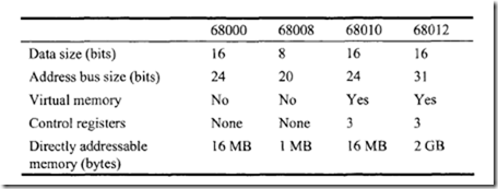
with all pins assigned or in a 68-pin quad pack or PGA (pin grid array) with some unused pins. The 68000 is also packaged in 68-terminal chip carrier. The 68008 is packed in a 48- pin dual in-line package, whereas the 68012 is packed in an 84-pin grid array. The 68008 provides the basic 68000 capabilities with inexpensive packaging. It has an 8-bit data bus, which facilitates the interfacing of this chip to inexpensive 8-bit peripheral chips. The 680 I 0 provides hardware-based virtual memory support and efficient l00ping instructions. Like the 68000, it has a 16-bit data bus and a 24-bit address bus. The 68012 includes all the 68010 features with a 31-bit address bus. The clock frequencies of the 68008, 68010, and 68012 are the same as those of the 68000. The following table summarizes the basic differences among the 68000 family members:

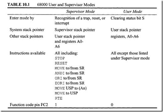
imageTo implement operating systems and protection features, the 68000 can be operated in two modes: supervisor and user. The supervisor mode is also called the "operating system mode." In this mode, the 68000 can execute all instructions. The 68000 operates in one of these modes based on the S bit of the status register. When the S bit is 1, the 68000 operates in the supervisor mode; when the S bit is 0, the 68000 operates in the user mode.

Table 10.1 lists the basic differences between the 68000 user and supervisor modes. From Table I 0.1, it can be seen that the 68000 executing a program in the supervisor mode can enter the user mode by modifying the S bit of the status register to 0 via an instruction. Instructions such as MOVE to SR, ANDI to SR, and EORI to SR can be used to accomplish this. On the other hand, the 68000 executing a program in the user mode can enter the supervisor mode only via recognition of a trap, reset, or interrupt. Note that, upon hardware reset, the 68000 operates in the supervisor mode and can execute all instructions. An attempt to execute privileged instructions (instructions that can only be execut.ed in the supervisor mode) in the user mode will automatically generate an internal interrupt (trap) by the 68000.

The logical level in the 68000 function code pin (FC2) indicates to the external devices whether the 68000 is currently operating in the user or supervisor mode. The 68000 has three function code pins (FC2, FC1, and FCO), which indicate to the external devices whether the 68000 is accessing supervisor program/data or user program/data or performing an interrupt acknowledge cycle.

The 68000 can operate on five different data types: bits, 4-bit binary-coded decimal (BCD) digits, bytes, 16-bit words, and 32-bit long words. The 68000 instruction set includes 56 basic instruction types. With 14 addressing modes, 56 instructions, and 5 data types, the 68000 contains over I 000 op-codes. The fastest instruction is one that copies the contents of one register into another register. It is executed in 500 ns at an 8- MHz clock rate. The slowest instruction is 32-bit by 16-bit divide, which in executed in 1.25 JlS at 8 MHz. The 68000 has no I/O instructions. Thus, the I/O is memory mapped.

image

Hence, MOVE instructions between a register and a memory address are also used as I/O instructions. The MC68000 is a general-purpose register-based microprocessor. Although the 68000 PC is 32 bits wide, only the low-order 24 bits are used. Because this is a byte-

image

addressable machine, it follows that the 68000 microprocessor can directly address 16 MB of memory. Note that symbol [ ] is used in the examples throughout this chapter to indicate the contents of a 68000 register or a memory location.

10.2 68000 Registers

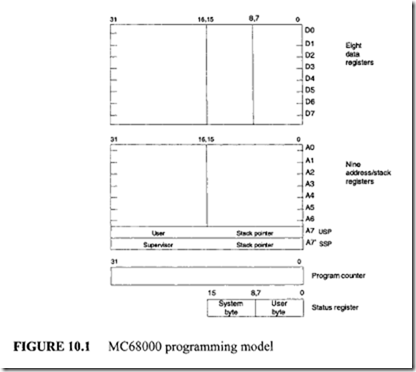
Figure 10.1 shows the 68000 registers. This microprocessor includes eight 32-bit data registers (DO-D7) and nine 32-bit address registers (AO-A 7 plus A 7′). Data registers normally hold data items such as 8-bit bytes, 16-bit words, and 32-bit long words. An address register usually holds the memory address of an operand; AO-A6 can be used as 16- or 32-bit. Because the 68000 uses 24-bit addresses, it discards the uppermost 8 bits (bits 24-31) while using the address registers to hold memory addresses. The 68000 uses A7 or A7′ as the user or supervisor stack pointer (USP or SSP), respectively, depending on the mode of operation.

The 68000 status register is composed of two bytes: a user byte and a system byte (Figure 10.2). The user byte includes typical condition codes such as C, V, N, Z, and X. The meaning of the C, V, N, and Z flags is obvious. Let us explain the meaning of the X bit. Note that the 68000 does not have any ADDC or SUBC instructions; rather, it has ADDX and sUBX instructions.

Because the flags C and X are usually affected in an identical manner, one can use ADDX or SUBX to reflect the carries or borrows in multiprecision arithmetic. The contents of the system byte include a 3-bit interrupt mask (12, II, 10), a supervisor flag (S), and a trace flag (T). When the supervisor flag is 1, then the system operates in the supervisor mode; otherwise, the user mode of operation is assumed. When the trace flag is set to 1, the processor generates a trap (internal interrupt) after executing each instruction. A debugging routine can be written at the interrupt address vector to display registers and/or memory after execution of each instruction. Thus, this will provide a single-stepping facility. Note that the trace flag can be set to one in the supervisor mode by executing the instruction ORI# $8000, SR.

The interrupt mask bits (12, I I, 10) provide the status of the 68000 interrupt pins IPL2, IPLI and IPLO. 12 II 10 = 000 indicates that all interrupts are enabled. 12 II 10 = 111 indicates that all maskable interrupts except the nonrnaskable interrupt (Level 7) are disabled. The other combinations of 12, 11, and 10 provide the maskable interrupt levels. Note that the signals on the IPL2, IPLI and IPL0 pins are inverted internally and then compared with 12, II, and 10, respectively.

image

image

10.3 68000 Memory Addressing

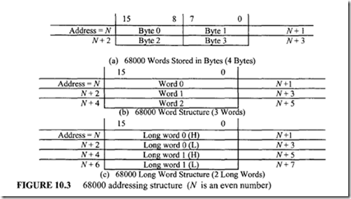
The MC68000 supports bytes (8 bits), words (16 bits), and long words (32 bits) as shown in Figure I 0.3. Byte addressing includes both odd and even addresses (0, I, 2, 3, …), word addressing includes only even addresses in increments of 2 (0, 2, 4, …), and long word addressing contains even addresses in increments of 4 (0, 4, 8, …). As an example of 68000 addressing structure, consider MOVE • L D 0 , $50 6 0 8 0 . If [DO] == $07F 12481, then after this MOVE, [$506080] == $07, [$50608I] = $Fl, [$506082] = $24, and [$506083)

= $81. In the 68000, all instructions must be located at even addresses for byte, word, and

long word instructions; otherwise, the 68000 generates an internal interrupt. The size of each 68000 instruction is even multiples of a byte. This means that once the programmer writes a program starting at an even address, all instructions are located at even addresses after assembling the program. For byte instructions, data can be located at even or odd addresses. On the other hand, data for word and long word instruction must be located at even addresses; otherwise the 68000 generates an internal interrupt.

Note that in 68000 for word and long word data, the low-order address stores the high-order byte of a number. This is called Big-endian byte ordering.

10.4 68000 Addressing Modes

The 14 addressing modes of the 68000 shown in Table 10.2 can be divided into 6 basic groups: register direct, address register indirect, absolute, program counter relative, immediate, and implied.

As mentioned, the 68000 has three types of instructions: no operand, single operand, and double operand. The single-operand instructions contain the effective address (EA) in the operand field. The EA for these instructions is calculated by the 68000 using the addressing mode used for this operand. In the case of two-operand instructions, one of the operands usually contains the EA and the other operand is usually a register or memory location. The EA in these instructions is calculated by the 68000 based on the addressing

image

mode used for the EA.

Some two-operand instructions have the EA in both operands. This means that the operands in these instructions use two addressing modes. Note that the 68000 address registers do not support byte-sized operands. Therefore, when an address register is used as a source operand, either the low-order word or the entire long word operand is used, depending on the operation size. When an address register is used as the destination operand, the entire register is affected regardless of operation size. If the operation size is a word, an address register in the destination operand is sign-extended to 32 bits after the operation is performed. Data registers, on t!1e Jther hand, support data operands of byte, word, or long word size.

To identify the operand size of an instruction, the following notation is placed after a 68000 mnemonic: .B for byte, .W or none (default) for word, and .L for long word. For example,

image

10.4.1 Register Direct Addressing

In this mode, the eight data registers (DO-D7) or seven address registers (AO-A6) contain the data operand. For example, consider ADD. W $ 0 0 50 0 0, DO. The destination operand of this instruction is in data register direct mode. Now, if [005000] = 000216 and [DO.W] = 000316, then after execution of ADD $005000, DO, the contents ofDO.W = 0002 + 0003 = 0005. Note that in this instruction, the$ symbol is used by Motorola to represent hexadecimal numbers. Also note that instructions are not available for byte operations using address registers.

10.4.2 Address Register Indirect Addressing

There are five different types of address register indirect mode. In this mode, an address register contains the effective address. For example, consider CLR. W (Al). If [Al. L]=$00003000, then, after execution of CLR. W (Al) , the 16-bit contents of memory location $003000 will be cleared to zero.

The postincrement address register indirect mode increments an address register by 1 for byte, 2 for word, and 4 for long word after it is used. For example, consider CLR. L (AO) +. If[AO] = 00005000 16, then after execution ofCLR. L (AO) +,the 16-bit contents of each of the memory locations 005000 16 and 005002 16 are cleared to zero and [AO] = 00005000 + 4 = 00005004. The postincrement mode is typically used with memory arrays stored from LOW to HIGH memory locations. For example, to clear I 00016 words starting at memory location 003000 16 and above, the following instruction sequence can be used:

imageNote that the symbol# in the above is used by the Motorola assember to indicate the immediate mode. This will be discussed later in this section. Also, note that CLR. W (AO) + automatically points to the next location by incrementing AO by 2 after clearing a memory location.

The predecrement address register indirect mode, on the other hand, decrements an address register by 1 for byte, 2 for word, and 4 for long word before using a register. For example, consider CLR. W – (AO). If [AO] = $00002004, then the content of AO is first decremented by 2-that is, [AO] = 00002002 16. The content of memory location 002002 is then cleared to zero. The predecrement mode is used with arrays stored from HIGH to LOW memory locations. For example, to clear I 00016 words starting at memory location 004000 16 and below, the following instruction sequence can be used:

image

image

In this instruction sequence, CLR. w – (A0) first decrements A0 by 2 and then clears the location. Because the starting address is 004000 16, A0 must initially be loaded with 00004002 16• It should be pointed out that the predecrement and postincrement modes can be combined in a single instruction. A typical example is MOVE. W (AS)+ 1- (A3).

The two other address register modes provide accessing of the tables by allowing offsets and indexes to be included with an indirect address pointer. The address register indirect with offset mode determines the effective address by adding a 16-bit signed integer to the contents of an address register. For example, consider MOVE. W $10 (AS) 1 D3 in which the source operand is in address register indirect with offset mode. If [A5] = 00002000 16 and [002010]16 = 0014 16, then, after execution of MOVE. W $10 (AS), D3, register D3.W will contain 001416

The indexed register indirect with offset mode determines the effective address by adding an 8-bit signed integer and the contents of a register (data or address register) to the contents of an address (base) register. This mode is usually used when the offset from the base address register needs to be varied during program execution. The size of the index register can be a signed 16-bit integer or an unsigned 32-bit value. As an example, consider MOVE. W $10 (A4 1 D3. W) 1 D4 in which the source is in the indexed register indirect with offset mode. Note that in this instruction A4 is the base register and D3.W is the 16-bit index register (sign-extended to 32 bits). This register can be specified as 32 bits by using D3 .L in the instruction, and I 016 is the 8-bit offset that is sign-extended to 32 bits. If [A4] = 00003000 16, [D3.W] = 0200 16, and [00321016] = 002416, then this MOVE instruction will load 0024 16 into the low 16 bits of register D4.

The address register indirect with offset mode can be used to access a single table. The offset (maximum 16 bits) can be the starting address of the table (fixed number), and the address register can hold the index number in the table to be accessed. Note that the starting address plus the index number provides the address of the element to be accessed in the table. For example, consider MOVE .W $34 0 0 (AS) 1 D1. If A5 contains 04, then this MOVE instruction transfers the contents of 3404 (i.e. the fifth element, 0 being the first element) into the low 16 bits of D 1. The indexed register indirect with offset mode, on the other hand, can be used to access multiple tables. Here, the offset (maximum 8 bits) can be the element number to be accessed. The address register pointer can be used to hold the starting address of the table containing the lowest starting address, and the index register can be used to hold the difference between the starting address of the table being accessed and the table with the lowest starting address. For example, consider three tables, with table I starting at 002000 16, table 2 at 003000 16, and table 3 at 004000 16. To transfer

the seventh element (0 being the first element) in table 2 to the low 16 bits of register D0,

the instruction MOVE .W $ 0 6 ( A2 , D1.W) 1 D0 can be used, where [A2] = the starting address of the table with the lowest address(= 002000 16 in this case) and [D How 16 bits =the difference between the starting address of the table being accessed and the starting address of the table with the lowest address= 003000 16 – 002000 16 = l 00016• Therefore, this MOVE instruction will transfer the contents of address 003006 16 (the seventh element in table 2) to register DO. The indexed register indirect with offset mode can also be used to access two-dimensional arrays such as matrices.

10.4.3 Absolute Addressing

In this mode, the effective address is part of the instruction. The 68000 has two modes: absolute short addressing, in which a 16-bit address is used (the address is sign-extended to 24 bits before use), and absolute long addressing, in which a 24-bit address is used. For example, consider ADD $2 0 0 0, D2 as an example of the absolute short mode. If [$002000] = 001216 and [D2.W] = 001016,then, after executing ADD $2 0 0 0, D2, register D2.W will contain 002216• The absolute long addressing mode is used when the address size is more than 16 bits. For example, MOVE • W $2 4 0 0 0 0 , D 5 loads the 16-bit contents of memory location 240000 16 into the low 16 bits ofD5. The absolute short mode includes an address ADDR in the range of O s ADDR s $7FFF or $FF8000 s ADDR s $FFFFFF. Note that a single instruction may use both short and long absolute modes, depending on whether the source or destination address is less than, equal to, or greater than the 16-bit address. A typical example is MOVE .w $50 0 0 0 2 , $10 0 0. Also, note that the absolute long mode must be used for MOVE to or from address $008000. For example, MOVE. W $8000,D1 will move the 16-bit contents of location $FF8000 to D1 while MOVE. W $008000,D 1 will transfer the 16-bit contents of address $008000 to D 1.

10.4.4 Program Counter Relative Addressing

The 68000 has two program counter relative addressing modes: relative with offset and relative with index and offset. In the relative with offset mode, the effective address is obtained by adding the contents of the current PC with a signed 16-bit displacement. This mode can be used when the displacement needs to be fixed during program execution. Typical branch instructions such as BEQ, BRA, and BLE use the relative with offset mode. This mode can also be used by some other instructions. For example, consider ADD $30 (PC) , D5, in which the source operand is in the relative with offset mode. Now suppose that the current PC contents is $002000, the content of 002030 16 is 0005, and the low 16 bits of D5 contain 001016• Then, after execution of this ADD instruction, D5 will contain 001516

In the relative with index and offset mode, the effective address is obtained by adding the contents of the current PC, a signed 8-bit displacement (sign-extended to 32 bits), and the contents of an index register (address or data register). The size of the index register can be 16 or 32 bits wide. For example, consider ADD. W $4 (PC, DO. W), D2. If [D2] = 00000012 16, [PC]= 002000 16, [D0]10w 16 bits = 001016,and [002014] = 000216, then, after this ADD, [D2]1ow 16 bits= 001416• This mode is used when the displacement needs to be changed during program execution by modifying the content of the Index register.

An advantage of the relative mode is that the destination address is specified relative to the address of the instruction after the instruction. Since the 68000 instructions with relative mode do not contain an absolute address, the program can be placed anywhere in memory which can still be excuted properly by the 68000. A program which can be placed anywhere in memory, and can still run correctly is called a "relocatable" program. It is a good practice to write relocatable programs.

10.4.5 Immediate Data Addressing

Two immediate modes are available with the 68000: immediate and quick immediate modes. In immediate mode, the operand data is constant data, which is part of the instruction. For example, consider ADDI. w #$0005, D0. If [DO.W] = 000216, then, after this ADDI instruction, [DO.W] = 0002 16 + 000516 = 000716• Note that the# symbol is used by Motorola to indicate the immediate mode. Quick immediate (ADD or SUBTRACT) mode allows

image


one to increment or decrement a register or a memory location (.B, .W, .L) by a number from 0 to 7. For example, ADDQ. B #1, D0 increments the low 8-bit contents of D0 by 1. Note that immediate data, 1 is inherent in the instruction. That is, data 0 to 7 is contained in the three bits of the instruction. Note that ADDQ.B #0, Dn is similar to NOP instruction.

10.4.6 Implied Addressing

The instructions using implied addressing mode do not require any operand, and registers such as PC, SP, or SR are referenced in these instructions. For example, RTS returns to the main program from a subroutine by placing the return address into PC using the PC implicitly.

It should be pointed out that in the 68000 the first operand of a two-operand instruction is the source and the second operand is the destination. Recall that in the case of the 8086, the first operand is the destination and the second operand is the source.


Questions and problems

QUESTIONS AND PROBLEMS

9.1 What is the basic difference between the 8086, 8086-1, 8086-2, and 8086-4?

9.2 Assume (DS)=1000H, (SS)=2000H, (CS)=3000H, (BP)=OOOFH, (BX)=000AH before execution of the following 8086 instructions:

(a) MOV CX,[BX]                    (b) MOV DX,[BP]

Which instruction will be executed faster by the 8086, and why ?

9.3 What is the purpose of the 8086 MN/MX pin?

9.4 If (DS) = 205FH and OFFSET = 0052H, what is the 8086 physical address?

Does the EU or BIU compute this physical address?

9.5 In an 8086 system, SEGMENT 1 contains addresses 00100H-00200H and SEGMENT 2 also contains addresses 001OOH-00200H. What are these segments called?

9.6 Determine the addressing modes for the following 8086 instructions:

image

9.7 Find the overflow, direction, interrupt, trap, sign, zero, parity, and carry flags after execution of the following 8086 instruction sequence:

MOV AH, 0FH

SAHF

9.8 What is the content of AL after execution of the following 8086 instruction sequence?

MOV BH, 33H

MOV AL, 32H

ADD AL, BH

AAA

9.9 What happens after execution of the following 8086 instruction sequence?

Comment.

MOV           DX,     00lFH

XCHG         DL,      DH

MOV         AX,       DX

IDIV          DL

9.10 What are the remainder, quotient, and registers containing them after execution of the following 8086 instruction sequence?

MOV AH, 0

MOV AL, OFFH

MOV CX, 2

IDIV CL

9.11 Write an 8086 instruction sequence to set the trap flag for single stepping without affecting the other flags in the Status register.

9.12 Write an 8086 assembly language program to subtract two 64-bit numbers.

Assume SI and DI point to the low words of the numbers.

9.13 Write an 8086 assembly program to add a 16-bit number stored in BX (bits 0 to 7 containing the high-order byte of the number and bits 8 to 15 containing the low­ order byte) with another 16-bit number stored in ex (bits 0 to 7 containing the low-order 8 bits of the number and bits 8 thorough 15 containing the high-order 8 bits). Store the result in AX.

9.14 Write an 8086 assembly program to multiply the top two 16-bit unsigned words of the stack. Store the 32-bit result onto the stack.

9.15 Write an 8086 assembly language program to add three 16-bit numbers. Store the 16-bit result in AX.

9.16 Write an 8086 assembly language to find the area of a circle with radius 2 meters and save the result in AX.

9.17 Write an 8086 assembly language program to convert 255 degrees in Celsius in BL to Fahrenheit degrees and store the value in AX. Use the equation

F=(C/5)*9+32

9.18 Assume AL, CX and DXBX contain a signed byte, a signed word, and a signed 32-bit number respectively. Write an 8086 assembly language program that will compute the signed 32-bit result: AL – CX + DXBX –+ DXBX.

9.19 Write an 8086 assembly program to divide an 8-bit signed number in CH by an 8-bit signed number in CL. Store the quotient in CH and the remainder in CL.

9.20 Write an 8086 assembly program to add 25 16-bit numbers stored in consecutive memory locations starting at displacement 0100H in DS == 0020H. Store the 16- bit result onto the stack.

9.21 Write an 8086 assembly program to find the minimum value of a string of 10 signed 8-bit numbers using indexed addressing. Assume Offset 5000H contains the first number.

9.22 Write an 8086 assembly program to move 100 words from a source with offset 0010H in ES to a destination with offset 0100H in the same extra segment.

9.23 Write an 8086 assembly program to divide a 28-bit unsigned number in the high 28 bits of DX AX by 810• Do not use any divide instruction. Store the quotient in the low 28 bits of DX AX. Discard remainder.

9.24 Write an 8086 assembly program to compare two strings of 15 ASCII characters.

The first character (string 1) is stored starting at offset 5000H in DS followed by the string. The first character of the second string (string 2) is stored starting at 6000H in ES. The ASCII character in the first location of string 1 will be compared with the first ASCII character of string 2, and so on. As soon as a match is found, store OOEE 16 onto the stack; otherwise, store 000016 onto the stack.

9.25 Write a subroutine in 8086 assembly language that can be called up by a main program in a different code segment. The subroutine will compute the 16-bit sum

image

 Assume the X;’s are signed 8-bit numbers and are stored in consecutive locations starting at displacement 0050H. Also, write the main program that will call this subroutine to compute

imageand store the 16-bit result (8-bit remainder and 8-bit quotient) in two consecutive memory bytes starting at offset 0400H.

9.26 Write a subroutine in 8086 assembly language to convert a 2-digit unpacked BCD number to binary. The most significant digit is stored in a memory location starting at offset 4000H, and the least significant digit is stored at offset 4001H. Store the binary result in DL.Use the value of the 2-digit BCD number, V = D1 x 10 + D0 Note that  arithmetic operations will provide binary result.

9.27 Assume an 8086/2732/6116/8255 microcomputer. Suppose that four switches are connected at bits 0 through 3 of port A and an LED is connected at bit 4 of port B. If the number of LOW switches is even, tum the port B LED ON; otherwise, tum the port BLED OFF. Write an 8086 assembly language program to accomplish this. Do not use any instructions involving the Parity flag.

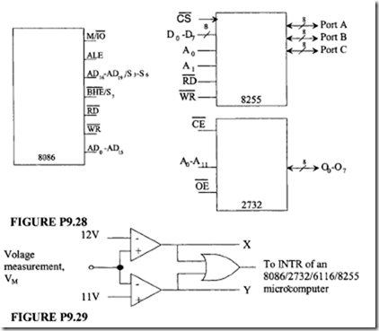
9.28 Interface two 2732 and one 8255 odd to an 8086 to obtain even and odd 2732 locations and odd addresses for the 8255’s port A, port B, port C, and control registers. Show only the connections for the pins shown in Figure P9.28. Assume all unused address lines to be zeros.

image

9.29 In Figure P9.29, if VM > 12 V, tum the LED ON connected at bit 4 of port A. On the other hand, if VM < 11 V, tum the LED OFF. Use ports, registers, and memory locations of your choice. Draw a hardware block diagram showing the microcomputer and the connections of the figure to its ports. Write a service routine in 8086 assembly language. Assume all segment registers are already initialized. The service routine should be written as CS=1000H, IP=2000H. The main program will initialize SP to 2050H, initialize ports, and wait for interrupts.

9.30 Repeat Problem 9.29 using the 8086 NMI interrupt.

9.31 An 8086/2732/6116/8255-based microcomputer is required to drive the LEDs connected to bit 0 of ports A and B based on the input conditions set by switches connected to bit 1 of ports A and B. The I/O conditions are as follows:

  • If the input at bit 1 of port A is HIGH and the input at bit 1 of port B is low, then the LED at port A will be ON and the LED at port B will be OFF.
  • If the input at bit 1 of port A is LOW and the input at bit 1 of port B is HIGH, then the LED at port A will be OFF and the LED at port B will be ON.
  • If the inputs at both ports A and B are the same (either both HIGH or both LOW), then both LEDs at ports A and B will be ON.

Write an 8086 assembly language program to accomplish this. Do not use any instructions involving the parity flag.

9.32 An 8086/2732/6116/8255-based microcomputer is required to test a NAND gate. Figure P9.32 shows the I/O hardware needed to test the NAND gate. The microcomputer is to be programmed to generate the various logic conditions for the NAND inputs, input the NAND output, and tum the LED ON connected to bit 3 of port A if the NAND gate chip is found to be faulty. Otherwise, tum the LED ON connected to bit 4 of port A. Write an 8086 assembly language program to accomplish this.

image

9.33 An 8086/2732/6116/8255 microcomputer is required to add two 3-bit numbers in AL and BL and output the sum (not to exceed 9) to a common cathode seven­ segment display connected to port A as shown in Figure P9.33.Write an 8086 assembly language program to accomplish this by using a look-up table. Do not use XLAT instruction.

9.34 Write an 8086 assembly language program to tum an LED OFF connected to bit 2 of port A of an 8086/2732/6116/8255 microcomputer and then turn it on after delay of 15 s. Assume the LED is ON initially.

9.35 What are the factors to be considered for interfacing a hex keyboard to a microcomputer?

9.36 An 8086/2732/6116/8255 microcomputer is required to input a number from 0 to 9 from an ASCII keyboard interfaced to it and output to an EBCDIC printer. Assume that the keyboard is connected to port A and the printer is connected to port B. Write an 8086 assembly language to accomplish this. Use XLAT instruction.

9.37 Will the circuit shown in Figure P9.37 work? If so, determine the I/O map in hex.

If not, justify briefly, modify the circuit and determine the I/O map in hex. Use only the pins and signals provided. Assume all don’t cares to be zeros. Note that I/O map includes the addresses for port A, port B, port C, and the control register. Using the logical port addresses, write an instruction sequence to configure port A as input and port B as output.

image


8086 I/O Ports , Important Points To Be Considered for 8086 Interface to Memory and I/O and 8086-Based Microcomputer

9.9.3 8086 I/O Ports

Devices with 8-bit I/O ports can be connected to either the upper or the lower half of the data bus. If the I/O port chip is connected to the lower half of the 8086 data lines (AD0- AD7), the port addresses will be even (A0 = 0). On the other hand, the port addresses will be odd (A0 = 1) if the I/O port chip is connected to the upper half of the 8086 data lines (AD8-AD 15). A0 will always be 1 or 0 for the partitioned I/O chip. Therefore, A0 cannot be used as an address input to select registers within a particular I/O chip. If two chips are connected to the lower and upper halves of the 8086 address bus that differ only in A0 (consecutive odd and even addresses), A0 and BHE must be used as conditions of chip select decoding to avoid a write to one I/O chip from erroneously performing a write to the other.

The 8086 uses either standard I/O or memory-mapped I/O. The standard I/O uses the instructions IN and OUT, and is able to provide up to 64K bytes of I/O locations. The standard I/O can transfer either 8-bit data or 16-bit data to or from a peripheral device. The 64-Kbyte I/O locations can then be configured as 64K 8-bit ports or 32K 16-bit ports. All I/O transfers between the 8086 and peripheral devices take place via AL for 8-bit ports (AH is not involved) and AX for 16-bit ports.

image

The I/O port addressing can be done either directly or indirectly as follows:

• Direct

IN AX, PORTA or IN AL, PORTA inputs 16-bit contents of port A into AX or 8-bit contents of port A into AL, respectively.

OUT PORTA, AX or OUT PORTA, AL outputs 16-bit contents of AX into port A or 8-hit contents of AL into port A, respectively.

• Indirect

IN AX, DX or IN AL, DX inputs 16-bit data into a port addressed by DX into AX or 8-bit data into a port addressed by DX into AL, respectively.

OUT DX, AX or OUT DX, AL outputs 16-bit contents of AX into a port addressed Mby DX or 8-bit contents of AL into a port addressed by DX, respectively.

Memory-mapped I/O is basically accomplished by using the memory instructions such as MOV AX or AL, [ BX] and MOV [ BX] , AX or AL for inputting or outputting, 8- or 16-bit data to/from AL or AX addressed by the 20-bit address computed from DS and BX. Note that any 8- or 16-bit general purpose register and memory modes can be used in memory-mapped I/O.

The 8086 programmed I/Ocapability will be explained in the following paragraphs using the 8255 I/O chip. The 8255 chip is a general-purpose programmable I/O chip. The 8255 has three 8-bit I/O ports: ports A, B, and C. Ports A and B are latched 8-bit ports for both input and output. Port C is also an 8-bit port with latched output, but the inputs are not latched. Port C can be used in two ways: It can be used either as a simple I/O port or as a control port for data transfer using handshaking via ports A and B.

The 8086 configures the three ports by outputting appropriate data to the 8-bit control register. The ports can be decoded by two 8255 input pins A0 and A,, as follows:

image 

Bit 7 (D7) of the control register must be 1 to send the definitions for bits 0-6 (D0-D6) as shown in the diagram. In this format, bits D0-D6, are divided into two groups: groups A and B. Group A configures all 8 bits of port A and the upper 4 bits of port C; group B defines all 8 bits of port B and the lower 4 bits of port C. All bits in a port can be configured as a parallel input port by writing a 1 at the appropriate bit in the control register by the 8086 OUT instruction, and a 0 in a particular bit position will configure the appropriate port as a parallel output port. Group A has three modes of operation: modes 0, 1, and 2. Group B has two modes: modes 0 and I. Mode 0 for both groups provides simple I/O operation for each of the three ports. No handshaking is required. Mode 1 for both groups is the strobed I/O mode used for transferring I/O data to or from a specified port in conjunction with strobes or handshaking signals. Ports A and B use the pins on port C to generate or accept these handshaking signals. Mode 2 of group A is the strobed bidirectional bus I/O and may be used for communicating with a peripheral device on a single 8-bit data bus for both transmitting and receiving data (bidirectional bus I/O). Handshaking signals are required. Interrupt generation and enable/disable functions are also available.

image


When D7 = 0, the bit set/reset control word format is used for the control register This format is used to set or reset the output on a pin of port Cor when enabling of the interrupt output signals for handshake data transfer is desired. For example, the 8 bits (OXXXllOO) will clear bit 6 of port C to zero. Note that the control word format can be output to the 8255 control register by using the 8086 OUT instruction. Now, let us define the control word format for mode 0 more precisely by means of a numerical example. Consider that the control word format is 100000102 • With this data in the control register, all 8 bits of Port A are configured as outputs and the 8 bits of port C are also configured as outputs. All 8 bits of port B, however, are defined as inputs. On the other hand, outputting 100110112 into the control register will configure all three 8-bit ports (ports A, B, and C) as inputs.

9.9.4 Important Points To Be Considered for 8086 Interface to Memory and I/O

From the preceding discussions, the following points can be summarized:

1. For ROMs/EPROMs/PPROMs, BHE and A0 are not required as part of chip enable/select decoding.

2. For RAMs and I/O port chips, both BHE and A0 must be used in chip select logic.

3. For ROMs/EPROMs/PPROMs and RAMs, both even and odd chips are required.

However, for I/O chips, an odd-addressed I/O chip, an even-addressed I/O chip, or both can be used, depending on the number of ports required in an application. The 8086 BHE and/or A0 must be used in I/O chip select logic depending on the number and type (odd/even) of I/O chips used.

4. For interfacing ROMs/EPROMs/ PPROMs to the 8086, the same chip select logic must be used for both the even and its corresponding odd memory chip. The same thing applies to RAM and I/O chips except that both BHE and A0 must be

used for RAMs and I/O; however, this is applicable to I/O if both odd and even I/O chips are present in the system.

5. ROMs/EPROMs/PPROMs must be connected in such a way that the 8086 reset vector address FFFF0H is contained in the memory map.

Example 9.19

An 8086-8255-2732-6116-based microcomputer is required to drive an LED connected to bit 2 of port B based on two switch inputs connected to bits 6 and 7 of port A. If both switches are either HIGH or LOW, tum the LED ON; otherwise, tum it OFF. Assume a HIGH will tum the LED ON and a LOW will tum it OFF. Write an 8086 assembly language program to accomplish this.

Solution

image

Example 9.20

Write an 8086 assembly language program to drive an LED connected to bit 7 of port A based on a switch input at bit 0 of port A. If the switch is HIGH, tum the LED ON; otherwise, tum the LED OFF. Assume an 8086/2732/6116/8255 microcomputer. Also, write a C++ program to accomplish the same task. Compare the 68000 assembly program with the compiled assembly code. Comment on the result.

Solution

The 8086 assembly language program and the C++ program along with the compiled assembly code are shown below. The 8086 assembly program contains 11 instructions whereas the 8086 C++ code generates 16 instructions. This example illustrates that although C++ programming can handle I/O, it generates more codes than assembly language programming. Although programs in C++ are easier to write compared to assembly, the machine code generated by the equivalent assembly language is shorter. Also note that C++ programs are not 100 %portable while the same I/O programs are written using C++ for microprocessors by two different manufactures. This is because of the different hardware configurations (I/O and memory maps) for different manufacturers.

Note that the assembly language program can also be written by rotating bit 0 (switch input) of port A to bit 7 (LED output) of port A only once by using ROR AI, I rather than RCL AL,CL with [CL]=7. The equivalent C++ program will still generate more assembled codes than the assembly language program.

image

  • Assembly code generated from C++ code above using Microsoft DEBUG unassembler:
  • 8086/8255 Microcomputer C++ program for Switch and LED (C++ Compiler) of Example 9.20

image

image

image

image

9.10 8086-Based Microcomputer

In this section, an 8086 will be interfaced in minimum mode to provide 4K x 16 EPROM, 2K x 16 static RAM, and six 8-bit I/O ports. The 2732 EPROM, 6116 static RAM, and 8255 I/O chips are used for this purpose. Memory and I/O maps are determined. Figure

9.20 shows a hardware schematic for accomplishing this.

The power and ground pins of all chips must be connected together to the power supply’s power and ground pins. The 8086 MN/MX is connected to +5 V for minimum mode (single processor) operation. Linear decoding is used to select both EPROMs and SRAMs. 8086 demultiplexed A 13 = I is used to select 2732s and 8086 demultiplexed A 14 = 0 is used for 6116s. No unused address pin is used for selecting the 8255s because the 8086 M/IO pin distinguishes between memory and I/O.

Let us determine the 8086 memory and I/O maps. To determine the memory map for 2732 EPROMs, consider Figure 9.21 (obtained from Figure 9.20), which shows pertinent connections for the even 2732.

In Figure 9.20, M/10 = 1 when the 8086 executes a memory-oriented instruction such as MOV [ BX) , DL to access the memory. Also, in the figure, A 13 = 1 is used to select the EPROMs and A 14 = 1 is used to deselect the RAMs. This is done to include the 8086 reset vector FFFF0 16 in the EPROMs. Therefore, an inverter is used to invert A 13

image

image

from Figure 9.20), which shows pertinent connections for the even 8255. The 8086 outputs LOW on its M/IO pin (M/IO = 0) when it executes an IN or OUT instruction. The 8086 outputs LOW (A0 = 0) for an even port address. This will produce a LOW on the CS pin of the even 8255. The even 8255 will thus be selected.

Using 8086 A 1 and A2 pins for port addresses, the I/O map for the even 8255 chip can be determined as follows:

image


Interfacing an 8086-Based Microcomputer to a Hexadecimal Keyboard and Seven-Segment Displays , Basics of Keyboard and Display Interface to a Microcomputer and Hex Keyboard Interface to an 8086-Based Microcomputer

9.12 Interfacing an 8086-Based Microcomputer to a Hexadecimal Keyboard and Seven-Segment Displays

This section describes the characteristics of the 8086-based microcomputer used with a hexadecimal keyboard and a seven-segment display.

9.12.1 Basics of Keyboard and Display Interface to a Microcomputer

A common method of entering programs into a microcomputer is via a keyboard. A popular way of displaying results by the microcomputer is by using seven-segment displays. The main functions to be performed for interfacing a keyboard are:

  • Sense a key actuation.
  • Debounce the key.
  • Decode the key.

Let us now elaborate on keyboard interfacing concepts. A keyboard is arranged in rows and columns. Figure 9.28 shows a 2 x 2 keyboard interfaced to a typical microcomputer. In Figure 9.28, the columns are normally at a HIGH level. A key actuation is sensed by sending a LOW (closing the diode switch) to each row one at a time via PAO and PAl of port A. The two columns can then be input via PB2 and PB3 of port B to see whether any of the normally HIGH columns are pulled LOW by a key actuation. If so, the rows can be

image

checked individually to determine the row in which the key is down. The row and column code for the pressed key can thus be found.

The next step is to debounce the key. Key bounce occurs when a key is pressed or released-it bounces for a short time before making the contact. When this bounce occurs, it may appear to the microcomputer that the same key has been actuated several times instead of just once. This problem can be eliminated by reading the keyboard after about 20 ms and then verifying to see if it is still down. If it is, then the key actuation is valid. The next step is to translate the row and column code into a more popular code such as hexadecimal or ASCII. This can easily be accomplished by a program. Certain characteristics associated with keyboard actuations must be considered while interfacing to a microcomputer. Typically, these are two-key lockout and N-key rollover. The two-key lockout ensures that only one key is pressed. An additional key depressed and released does not generate any codes. The system is simple to implement and most often used. However, it might slow down the typing because each key must be fully released before the next one is pressed down. On the other hand, the N-key rollover will ignore all keys pressed until only one remains down.

Now let us elaborate on the interfacing characteristics of typical displays. The following functions are typically performed for displays:

I. Output the appropriate display code.

2. Output the code via right entry or left entry into the displays if there are more than one displays.

These functions can easily be realized by a microcomputer program. If there are more than one display, the displays are typically arranged in rows. A row of four displays is shown in Figure 9.29. In the figure, one has the option of outputting the display code via right entry or left entry. If the code is entered via right entry, the code for the least significant digit of the four-digit display should be output first, then the next digit code, and so on. The program outputs to the displays are so fast that visually all four digits will appear on the display simultaneously. If the displays are entered via left entry, then the most significant digit must be output first and the rest of the sequence is similar to the right entry.

Two techniques are typically used to interface a hexadecimal display to the microcomputer: nonmultiplexed and multiplexed. In nonmultiplexed methods, each hexadecimal display digit is interfaced to the microcomputer via an I/O port. Figure

9.30 illustrates this method. BCD to seven-segment conversion is done in software.

The microcomputer can be programmed to output to the two display digits in sequence. However, the microcomputer executes the display instruction sequence so fast that the displays appear to the human eye at the same time. Figure 9.31 illustrates the multiplexing method of interfacing the two hexadecimal displays to the microcomputer. In the multiplexing scheme, appropriate seven-segment code is sent to the desired displays on

image

seven lines common to all displays. However, the display to be illuminated is grounded. Some displays such as Texas Instrument’s TIL 311 have on-chip decoder. In this case, the microcomputer is required to output four bits (decimal) to a display.

The keyboard and display interfacing concepts described here can be realized by either software or hardware. To relieve the microprocessor of these functions, microprocessor manufacturers have developed a number of keyboard/display controller chips. These chips are typically initialized by the microprocessor. The keyboard/display functions are then performed by the chip independent ofthe microprocessor. The amount of keyboard/display functions performed by the controller chip varies from one manufacturer to another. However, these functions are usually shared between the controller chip and the microprocessor.

9.13.2 Hex Keyboard Interface to an 8086-Based Microcomputer

In this section, an 8086-based microcomputer is designed to display a hexadecimal digit entered via a keypad (16 keys). Figure 9.32 shows the hardware schematic.

I. Port A is configured as an input port to receive the row-column code.

2. Port B is configured as an output port to display the key(s) pressed.

3. Port Cis configured as an output port to output zeros to the rows to detect a key actuation.

The system is designed to run at 2 MHz. Debouncing is provided to avoid unwanted oscillation caused by the opening and closing of the key contacts. To ensure stability for the input signal, a delay of 20 ms is used for debouncing the input.

The program begins by performing all necessary initializations. Next, it makes sure that all the keys are opened (not pressed). A delay loop of 20 ms is included for debouncing, and the following instruction sequence is used (Section 9.8):

image

The next three lines detect a key closure. If a key closure is detected, it is debounced. It is necessary to determine exactly which key is pressed. To do this, a sequence of row-control codes (OFH, OEH, ODH, OBH, 07H) are output via port C. The row-column code is input via port A to determine if the column code changes corresponding to each different row code. If the column code is not OFH (changed), the input key is identified. The program then indexes through a look-up table to determine the row-column code saved in DL. If the code is found, the corresponding index value, which equals the input

image

key’s value (a single hexadecimal digit) is displayed. The program is written such that it will continuously scan for input key and update the display for each new input. Note that lowercase letters are used to represent the 8086 registers in the program. For example, al, ah, and ax in the program represent the 8086 AL, AH, and AX registers, respectively.

The memory and I/O maps are arbitrarily chosen. A listing of the 8086 assembly language program is given in the following:

image

image

In the program, the "Key-open" loop ensures that no keys are closed. On the other hand, the "Key-close" waits in the loop for a key actuation. Note that in this program, the table for the codes for the hexadecimal numbers 0 through F are obtained by inspecting Figure 9.32.

For example, consider key F. When key F is pressed and if a LOW is output by the program to bit 0 of port C, the top row and the rightmost column of the keyboard will be LOW. This will make the content of port A as:

image

Thus, a code of 7716 is obtained at Port A when the key F is pressed. Diodes are connected at the four bits (Bits 0-3) of Port C. This is done to make sure that when a 0 is output by the program to one of these bits (row of the keyboard), the diode switch will close and will generate a LOW on that row.

Now, if a key is pressed on a particular row which is LOW, the column connected to this key will also be LOW. This will enable the programmer to obtain the appropriate key code for each key.