8.1 Memory Organization
8.1.1 Introduction
A memory unit is an integral part of any microcomputer system, and its primary purpose is to hold instructions and data. The major design goal of a memory unit is to allow it to operate at a speed close to that of the processor. However, the cost of a memory unit is so prohibitive that it is practically not feasible to design a large memory unit with one technology that guarantees a high speed. Therefore, in order to seek a trade-off between the cost and operating speed, a memory system is usually designed with different technologies such as solid state, magnetic, and optical.
In a broad sense, a microcomputer memory system can be divided into three
groups:
-
Processor memory
-
Primary or main memory
-
Secondary memory
Processor memory refers to a set of microprocessor registers. These registers are used to hold temporary results when a computation is in progress. Also, there is no speed disparity between these registers and the microprocessor because they are fabricated using the same technology. However, the cost involved in this approach limits a microcomputer architect to include only a few registers in the microprocessor. The design of typical registers is described in Chapters 5, 6 and 7.
Main memory is the storage area in which all programs are executed. The microprocessor can directly access only those items that are stored in main memory. Therefore, all programs must be within the main memory prior to execution. CMOS technology is normally used these days in main memory design. The size of the main memory is usually much larger than processor memory and its operating speed is slower than the processor registers. Main memory normally includes ROMs and RAMs. These are described in Chapter 6.
Electromechanical memory devices such as disks are extensively used as microcomputer’s secondary memory and allow storage of large programs at a low cost. These secondary memory devices access stored data serially. Hence, they are significantly slower than the main memory. Popular secondary memories include hard disk and floppy disk systems. Programs are stored on the disks in files. Note that the floppy disk is removable whereas the hard disk is not. Secondary memory stores programs in excess of the main memory. Secondary memory is also referred to as "auxiliary" or "virtual" memory. The microcomputer cannot directly execute programs stored in the secondary memory, so in order to execute these programs, the microcomputer must transfer them to its main memory by a program called the "operating system."
Programs in disk memories are stored in tracks. A track is a concentric ring of programs stored on the surface of a disk. Each track is further subdivided into several sectors. Each sector typically stores 512 or 1024 bytes of information. All secondary memories use magnetic media except the optical memory, which stores programs on a plastic disk. CD-ROM is an example of a popular optical memory used with microcomputer systems. The CD-ROM is used to store large programs such as a C++ compiler. Other state-of-the-art optical memories include CD-RAM, DVD-ROM and DVD-RAM. These optical memories are discussed in Chapter 1.
In the past, one of the most commonly used disk memory with microcomputer systems was the floppy disk. The floppy disk is a flat, round piece of plastic coated with magnetically sensitive oxide material. The floppy disk is provided with a protective jacket to prevent fingerprint or foreign matter from contaminating the disk’s surface. The 3Y2- inch floppy disk was very popular because of its smaller size and because it didn’t bend easily. All floppy disks are provided with an off-center index hole that allows the electronic system reading the disk to find the start of a track and the first sector.
The storage capacity of a hard disk varied from 10 megabytes (MB) in 1981 to hundreds of gigabytes (GB) these days. The 3 Y:z-inch floppy disk, on the other hand, can typically store 1.44 MB. Zip disks were an enhancement in removable disk technology providing storage capacity of I 00 MB to 750 MB in a single disk with access speed similar to the hard disk. Zip disk does not use a laser. Rather, it uses a magnetic-coated Myler inside, along with smaller read/write heads, and a rotational speed of 3000 rpm. The smaller heads allow the Zip drive to store programs using 2, 118 tracks per inch, compared to 135 tracks per inch on a floppy disk. Floppy disks are being replaced these days by USB (Universal Serial Bus) Flash memory. Note that USB is a standard connection for computer peripherals such as CD burners. Also, flash memory gets its name because the technology uses microchips that allow a section of memory cells called blocks to be erased in a single action called a "flash". USB flash memory offers much more storage capacity than floppy disks, and can typically store I 6 megabytes up to multiple gigabytes of information.
8.1.2 Main Memory Array Design
From the previous discussions, we notice that the main memory of a microcomputer is fabricated using solid-state technology. In a typical microcomputer application, a designer has to implement the required capacity by interconnecting several small memory chips. This concept is known as the "memory array design." In this section, we address this topic. We also show how to interface a memory system with a typical microprocessor.
Now let us discuss how to design ROM/RAM arrays. In particular, our discussion is focused on the design of memory arrays for a hypothetical microcomputer. The pertinent signals of a typical microprocessor necessary for main memory interfacing are shown in
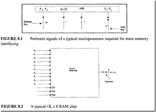 Figure 8.1. In Figure 8.1, there are 16 address lines, A 15 through ‘ with A0 being the least significant bit. This means that this microprocessor can directly address a maximum of 2 16
= 65,536 or 64K bytes of memory locations. The control line M/IO goes to LOW if the microprocessor executes an I/0 instruction, and it is held HIGH if the processor executes a memory instruction. Similarly, the control line R/W goes to HIGH to indicate that the operation is READ and it goes to LOW for WRITE operation. Note that all 16 address lines and the two control lines described so far are unidirectional in nature; that is, information can always travel on these lines from the processor to external units. Also, in Figure 8.1 eight bidirectional data lines D7 through D0 (with D0 being the least significant bit) are shown. These lines are used to allow data transfer from the processor to external units and vice versa.
In a typical application, the total amount of main memory connected to a microprocessor consists of a combination of both ROMs and RAMs. However, in the following we will illustrate for simplicity how to design memory array using only the RAM chips.
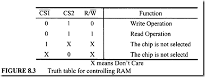
The pin diagram of a typical lK x 8 RAM chip is shown in Figure 8.2. In this RAM chip there are 10 address lines, A9 through A0, so one can read or write 1024 (210 = 1024) different memory words. Also, in this chip there are 8 bidirectional data lines D7 through D0 so that information can travel back and forth between the microprocessor and the memory unit. The three control lines CS 1, CS2, and RIW are used to control the RAM unit according to the truth table shown in Figure 8.3. From this truth table it can be concluded that the RAM unit is enabled only when CS 1 = 0 and CS2 = 1. Under this condition, RIW = 0 and R!W = 1 imply write and read operations respectively.
To connect a microprocessor to ROM/RAM chips, three address-decoding techniques are usually used: linear decoding, full decoding, and memory decoding using
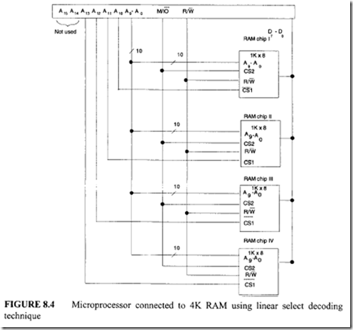
PLD. Let us first discuss how to interconnect a microprocessor with a 4K RAM chip array comprised of the four 1K RAM chips of Figure 8.2 using the linear decoding technique. Figure 8.4 uses the linear decoding to accomplish this.
In this approach, the address lines A9 through A0 of the microprocessor are connected to all RAM chips. Similarly, the control lines M/IO and RIW of the microprocessor are connected to the control lines CS2 and RIW respectively of each RAM chip. The high order address bits A 10 through A 13 directly act as chip selects.
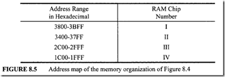
In particular, the address lines A 10 and A 11 select the RAM chips I and II respectively. Similarly, the address lines A 12 and A 13 select the RAM chips III and IV respectively. A 15 and A 14 are don’t cares and are assumed to be 0. Figure 8.5 describes how
the addresses are distributed among the four 1K RAM chips. This method is known as "linear select decoding," and its primary advantage is that it does not require any decoding hardware. However, if two or more lines of A 10 through A 13 are low at the same time, more than one RAM chip are selected, and this causes a bus conflict. Because of this potential problem, the software must be written in such a way that it never reads into or writes from any address in which more than one of the bits A 13 through A 10 are low. Another disadvantage of this method is that it wastes a large amount of address space. For example,
whenever the address value is 8800 or 3800, the RAM chip I is selected. In other words, the address 3800 is the mirror reflection of the address 8800 (this situation is also called "memory foldback"). This technique is, therefore, limited to a small system. In particular, we can extend the system of Figure 8.4 up to a total capacity of 6K using A 14 and A 15 as chip selects for two more 1K RAM chips.
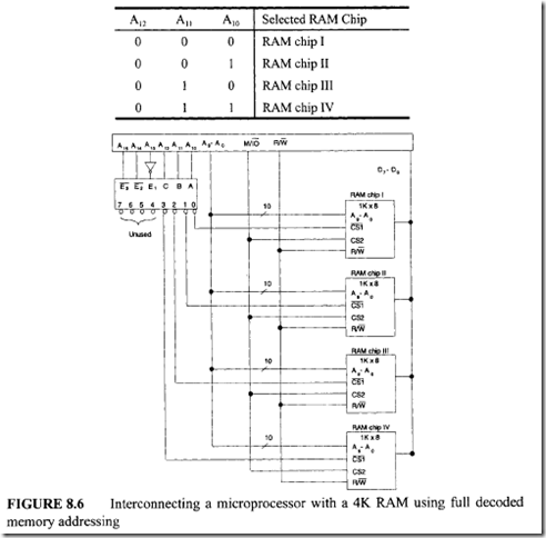
To resolve the problems with linear decoding, we use the full decoded memory
addressing. In this technique, we use a decoder. The same 4K memory system designed using this technique is shown in Figure 8.6. Note that the decoder in the figure is very similar to a practical decoder such as the 74LS138 with three chip enables. In Figure 8.6 the decoder output selects one of the four IK RAM chips depending on the values of A 12, A 11,and A 10• Note that the decoder output will be enabled only when E3 = E2 = 0 and El = I. Therefore, in the organization of Figure 8.6, when any one of the high-order bits A 15,A 14,
or A 13 is 1, the decoder will be disabled, and thus none of the RAM chips will be selected. In this arrangement, the memory addresses are assigned as shown in Figure 8.7.
This approach does not waste any address space since the unused decoder outputs (don’t cares) can be used for memory expansion. For example, the 3-to-8 decoder of Figure 8.6 can select eight lK RAM chips. Also, this method does not generate any bus conflict. This is because the selected decoder output ensures enabling of one memory chip at a time.
As mentioned before, a Programmable Logic Device (PLD) is similar to a ROM in concept except that it does not provide full decoding of the input lines. Instead, a PLD provides a partial sum of products that can be obtained via programming and saves a lot of space on the board. For example, a PAL chip contains a fused programmable AND array and a fixed OR array. Note that both AND and OR arrays are programmable in a PLA. The AND and OR gates are fabricated inside the PLD without interconnections. The specific functions desired are implemented during programming via software. For example, programming of the PAL provides connections of the AND gates to the inputs of the OR gates. Therefore, the PAL implements the sum of the products of the inputs. PLDs are used extensively these days with 32- and 64-bit microprocessors such as the Intel 80386/80486/Pentium and Motorola 68030/68040/PowerPC for performing the memory decode function. PLDs connect these microprocessors to memory, 1/0 devices, and other chips without the use of any additional logic gates or circuits.
