8254 PROGRAMMABLE INTERVAL TIMER
The 8254 programmable interval timer consists of three independent 16-bit programmable counters (timers). Each counter is capable of counting in binary or binary-coded decimal (BCD). The maximum allowable input frequency to any counter is 10 MHz. This device is useful wherever the microprocessor must control real time events. Some examples of usage include real-time clock and an events counter, and for motor speed and direction control.
This timer also appears in the personal computer decoded at ports 40H–43H to do the following:
1. Generate a basic timer interrupt that occurs at approximately 18.2 Hz.
2. Cause the DRAM memory system to be refreshed.
3. Provide a timing source to the internal speaker and other devices. The timer in the personal computer is an 8253 instead of an 8254.
8254 Functional Description
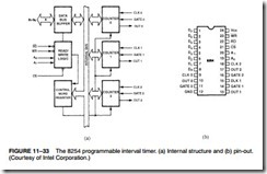
Figure 11–33 shows the pin-out of the 8254, which is a higher-speed version of the 8253, and a diagram of one of the three counters. Each timer contains a CLK input, a gate input, and an output (OUT) connection. The CLK input provides the basic operating frequency to the timer, the gate pin controls the timer in some modes, and the OUT pin is where we obtain the output of the timer.
The signals that connect to the microprocessor are the data bus pins (D7–D0), RD, WR, CS, and address inputs A1 and A0. The address inputs are present to select any of the four internal registers used for programming, reading, or writing to a counter. The personal computer contains an 8253 timer or its equivalent, decoded at I/O ports 40H–43H. Timer zero is programmed to generate an 18.2 Hz signal that interrupts the microprocessor at interrupt vector 8 for a clock tick. The tick is often used to time programs and events in DOS. Timer 1 is programmed for 15 μs, which is used on the personal computer to request a DMA action used to refresh the dynamic RAM. Timer 2 is programmed to generate a tone on the personal computer speaker.
Pin Definitions
A0, A1 The address inputs select one of four internal registers within the 8254. See Table 11–4 for the function of the A1 and A0 address bits.
CLK The clock input is the timing source for each of the internal counters. This input is often connected to the PCLK signal from the microprocessor system bus controller.
CS Chip select enables the 8254 for programming and reading or writing a counter.
G The gate input controls the operation of the counter in some modes of operation.
GND Ground connects to the system ground bus.
OUT A counter output is where the waveform generated by the timer is available.
RD Read causes data to be read from the 8254 and often connects to the IORC signal.
Vcc Power connects to the +5.0 V power supply.
WR Write causes data to be written to the 8254 and often connects to the write strobe (IOWC).
Programming the 8254
Each counter is individually programmed by writing a control word, followed by the initial count. Figure 11–34 lists the program control word structure of the 8254. The control word allows the programmer to select the counter, mode of operation, and type of operation (read/write). The control word also selects either a binary or BCD count. Each counter may be programmed with a count of 1 to FFFFH. A count of 0 is equal to FFFFH+l (65,536) or 10,000
in BCD. The minimum count of 1 applies to all modes of operation except modes 2 and 3, which have a minimum count of 2. Timer 0 is used in the personal computer with a divide-by count of 64K (FFFFH) to generate the 18.2 Hz (18.196 Hz) interrupt clock tick. Timer 0 has a clock input frequency of 4.77 MHz + 4 or 1.1925 MHz.
The control word uses the BCD bit to select a BCD count (BCD = 1) or a binary count (BCD = 0). The M2, M1, and M0 bits select one of the six different modes of operation (000–101) for the counter. The RW1 and RW0 bits determine how the data are read from or written to the counter. The SC1 and SC0 bits select a counter or the special read-back mode of operation, discussed later in this section.
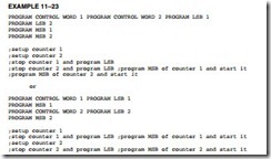
Each counter has a program control word used to select the way the counter operates. If two bytes are programmed into a counter, then the first byte (LSB) will stop the count, and the second byte (MSB) will start the counter with the new count. The order of programming is important for each counter, but programming of different counters may be interleaved for better control. For example, the control word may be sent to each counter before the counts for individual programming. Example 11–23 shows a few ways to program counters 1 and 2. The first method programs both control words, then the LSB of the count for each counter, which stops them from counting. Finally, the MSB portion of the count is programmed, starting both counters with the new count. The second example shows one counter programmed before the other.
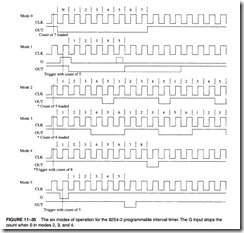
Modes of Operation. Six modes (mode 0–mode 5) of operation are available to each of the 8254 counters. Figure 11–35 shows how each of these modes functions with the CLK input, the gate (G) control signal, and OUT signal. A description of each mode follows:
MODE 0 Allows the 8254 counter to be used as an events counter. In this mode, the output becomes a logic 0 when the control word is written and remains there until N plus the number of programmed counts. For example, if a count of 5 is programmed, the output will remain a logic 0 for 6 counts beginning with N. Note that the gate (G) input must be a logic 1 to allow the counter to count. If G becomes a logic 0 in the middle of the count, the counter will stop until G again becomes a logic 1.
MODE 1 Causes the counter to function as a retriggerable, monostable multivibrator (one-shot). In this mode the G input triggers the counter so that it develops a pulse at the OUT connection that becomes a logic 0 for the duration of the
count. If the count is 10, then the OUT connection goes low for 10 clocking periods when triggered. If the G input occurs within the duration of the out- put pulse, the counter is again reloaded with the count and the OUT connection continues for the total length of the count.
MODE 2 Allows the counter to generate a series of continuous pulses that are one clock pulse wide. The separation between pulses is determined by the count. For example, for a count of 10, the output is a logic 1 for nine clock periods and low for one clock period. This cycle is repeated until the counter is programmed with a new count or until the G pin is placed at a logic 0 level. The G input must be a logic 1 for this mode to generate a continuous series of pulses.
MODE 3 Generates a continuous square wave at the OUT connection, provided that the G pin is a logic 1. If the count is even, the output is high for one half of the count and low for one half of the count. If the count is odd, the output is high for one clocking period longer than it is low. For example, if the counter is programmed for a count of 5, the output is high for three clocks and low for two clocks.
MODE 4 Allows the counter to produce a single pulse at the output. If the count is programmed as a 10, the output is high for 10 clocking periods and low for one clocking period. The cycle does not begin until the counter is loaded with its complete count. This mode operates as a software triggered one- shot. As with modes 2 and 3, this mode also uses the G input to enable the counter. The G input must be a logic 1 for the counter to operate for these three modes.
MODE 5 A hardware triggered one-shot that functions as mode 4, except that it is started by a trigger pulse on the G pin instead of by software. This mode is also similar to mode 1 because it is retriggerable.
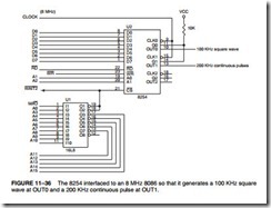
Generating a Waveform with the 8254. Figure 11–36 shows an 8254 connected to function at I/O ports 0700H, 0702H, 0704H, and 0706H of an 80386SX microprocessor. The addresses are decoded by using a PLD that also generates a write strobe signal for the 8254, which is connected to the low-order data bus connections. The PLD also generates a wait signal for the microprocessor that causes two wait states when the 8254 is accessed. The wait state generator connected to the microprocessor actually controls the number of wait states inserted into the timing. The program for the PLD is not illustrated here because it is the same as many of the prior examples.
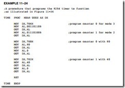
Example 11–24 lists the program that generates a 100 KHz square-wave at OUT0 and a 200 KHz continuous pulse at OUT1. Counter 0 uses mode 3 and counter 1 uses mode 2. The count programmed into counter 0 is 80 and the count for counter 1 is 40. These counts generate the desired output frequencies with an 8 MHz input clock.
Reading a Counter. Each counter has an internal latch that is read with the read counter port operation. These latches will normally follow the count. If the contents of the counter are needed, then the latch can remember the count by programming the counter latch control word (see Figure 11–37), which causes the contents of the counter to be held in a latch until they is read. Whenever a read from the latch or the counter is programmed, the latch tracks the contents of the counter.
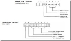
When it is necessary for the contents of more than one counter to be read at the same time, we use the read-back control word, illustrated in Figure 11–38. With the read-back control word, the CNT bit is a logic 0 to cause the counters selected by CNT0, CNT1, and CNT2 to be latched. If the status register is to be latched, then the ST bit is placed at a logic 0. Figure 11–39 shows the status register, which shows the state of the output pin, whether the counter is at its null state (0), and how the counter is programmed.
DC Motor Speed and Direction Control
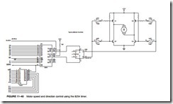
One application of the 8254 timer is as a motor speed controller for a DC motor. Figure 11–40 shows the schematic diagram of the motor and its associated driver circuitry. It also illustrates the interconnection of the 8254, a flip-flop, and the motor and its driver.
The operation of the motor driver circuitry is straightforward. If the Q output of the 74ALS112 is a logic 1, the base Q2 is pulled up to +12 V through the base pull-up resistor, and the base of Q2 is open circuited. This means that Q1 is off and Q2 is on, with ground applied to the positive lead of the motor. The bases of both Q3 and Q4 are pulled low to ground through the inverters. This causes Q3 to conduct or turn on and Q4 to turn off, applying ground to the negative lead of the motor. The logic 1 at the Q output of the flip-flop therefore connects +12 V to the positive lead of the motor and ground to the negative lead. This connection causes the motor to spin in its forward direction. If the state of the Q output of the flip-flop becomes a logic 0, then the conditions of the transistors are reversed and +12 V is attached to the negative lead of the motor, with ground attached to the positive lead. This causes the motor to spin in the reverse direction.
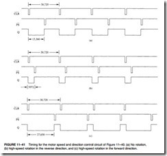
If the output of the flip-flop is alternated between a logic 1 and 0, the motor spins in either direction at various speeds. If the duty cycle of the Q output is 50%, the motor will not spin at all and exhibits some holding torque because current flows through it. Figure 11–41 shows some timing diagrams and their effects on the speed and direction of the motor. Notice how each counter generates pulses at different positions to vary the duty cycle at the Q output of the flip- flop. This output is also called pulse width modulation To generate these wave forms, counters 0 and 1 are both programmed to divide the input clock (PCLK) by 30,720. We change the duty cycle of Q by changing the point at which
counter 1 is started in relationship to counter 0. This changes the direction and speed of the motor. But why divide the 8 MHz clock by 30,720? The divide rate of 30,720 is divisible by 256, so we can develop a short program that allows 256 different speeds. This also produces a basic operating frequency for the motor of about 260 Hz, which is low enough in frequency to power the motor. It is important to keep this operating frequency below 1000 Hz, but above 60 Hz.
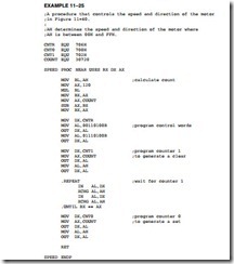
Example 11–25 lists a procedure that controls the speed and direction of the motor. The speed is controlled by the value of AH when this procedure is called. Because we have an 8-bit number to represent speed, a 50% duty cycle, for a stopped motor, is a count of 128. By chang- ing the value in AH when the procedure is called, we can adjust the motor speed. The speed of the motor will increase in either direction by changing the number in AH when this procedure is called. As the value in AH approaches 00H, the motor begins to increase its speed in the reverse direction. As the value of AH approaches FFH, the motor increases its speed in the forward direction.
The procedure adjusts the wave form at Q by first calculating the count at which counter 0 is to start in relationship to counter 1. This is accomplished by multiplying AH by 120 and then subtracting it from 30,720. This is required because the counters are down-counters that count from the programmed count to 0 before restarting. Next, counter 1 is programmed with a count of 30,720 and started so it generates the clear-wave form for the flip-flop. After counter 1 is started, it is read and compared with the calculated count. Once it reaches this count, counter 0 is started with a count of 30,720. From this point forward, both counters continue generating the clear and set wave forms until the procedure is again called to adjust the speed and direction of the motor.
