THE PROGRAMMABLE PERIPHERAL INTERFACE
The 82C55 programmable peripheral interface (PPI) is a very popular, low-cost interfacing component found in many applications. This is true even with all the programmable devices avail- able for simple applications. The PPI, which has 24 pins for I/O that are programmable in groups of 12 pins, has groups that operate in three distinct modes of operation. The 82C55 can interface any TTL-compatible I/O device to the microprocessor. The 82C55 (CMOS version) requires the insertion of wait states if operated with a microprocessor using higher than an 8 MHz clock. It also pro- vides at least 2.5 mA of sink (logic 0) current at each output, with a maximum of 4.0 mA. Because I/O devices are inherently slow, wait states used during I/O transfers do not impact significantly upon the speed of the system. The 82C55 still finds application (compatible for programming, although it may not appear in the system as a discrete 82C55), even in the latest Core2-based computer system. The modern computer uses a few 82C55s located inside the chip set for various features on the personal computer. The 82C55 is used for interface to the keyboard and the parallel printer port in many personal computers, but it is found as a function within a interfacing chip set. The chip set also controls the timer and reads data from the keyboard interface.
A low-cost experimentation board is available that plugs into the parallel port of a PC that allows access to an 8255 located on the board. The 8255 is programmed in either assembly language or Visual C++ through drivers available with the board. Visit the following Internet link for pricing and additional information:
http://www.microdigitaled.com/hardware/mdelpt/MDELPT.htm.
Basic Description of the 82C55
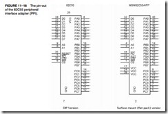
Figure 11–18 illustrates the pin-out diagram of the 82C55 in both the DIP format and the surface mount (flat pack). Its three I/O ports (labeled A, B, and C) are programmed as groups. Group A connections consist of port A (PA7–PA0) and the upper half of port C (PC7–PC4), and group B consists of port B (PB7–PB0) and the lower half of port C (PC3–PC0). The 82C55 is selected by its CS pin for programming and for reading or writing to a port. Register selection is accomplished through the A1 and A0 input pins that select an internal register for programming
or operation. Table 11–2 shows the I/O port assignments used for programming and access to the I/O ports. In the personal computer a pair of 82C55s, or their equivalents, are decoded at I/O ports 60H–63H and also at ports 378H–37BH.
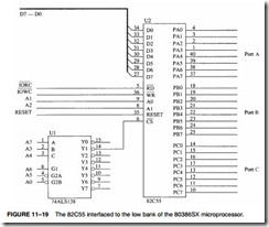
The 82C55 is a fairly simple device to interface to the microprocessor and program. For the 82C55 to be read or written, the CS input must be a logic 0 and the correct I/O address must be applied to the A1 and A0 pins. The remaining port address pins are don’t cares as far as the 82C55 is concerned, and are externally decoded to select the 82C55.
Figure 11–19 shows an 82C55 connected to the 80386SX so that it functions at 8-bit I/O port addresses C0H (port A), C2H (port B), C4H (port C), and C6H (command register). This interface uses the low bank of the 80386SX I/O map. Notice from this interface that all the 82C55 pins are direct connections to the 80386SX, except for the CS pin. The CS pin is decoded and selected by a 74ALS138 decoder.
The RESET input to the 82C55 initializes the device whenever the microprocessor is reset. A RESET input to the 82C55 causes all ports to be set up as simple input ports using mode 0 operation. Because the port pins are internally programmed as input pins after a RESET, damage is prevented when the power is first applied to the system. After a RESET, no other commands are needed to program the 82C55, as long as it is used as an input device for all three ports. Note
that an 82C55 is interfaced to the personal computer at port addresses 60H–63H for keyboard control, and also for controlling the speaker, timer, and other internal devices such as memory expansion. It is also used for the parallel printer port at I/O ports 378H–37BH.
Programming the 82C55
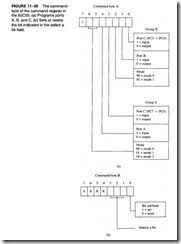
The 82C55 is programmed through the two internal command registers that are illustrated in Figure 11–20. Notice that bit position 7 selects either command byte A or command byte B. Command byte A programs the function of group A and B, whereas command byte B sets (1) or resets (0) bits of port C only if the 82C55 is programmed in mode 1 or 2.
Group B pins (port B and the lower part of port C) are programmed as either input or output pins. Group B operates in either mode 0 or mode 1. Mode 0 is the basic input/output mode that allows the pins of group B to be programmed as simple input and latched output connections. Mode 1 operation is the strobed operation for group B connections, where data are transferred through port B and handshaking signals are provided by port C.
Group A pins (port A and the upper part of port C) are programmed as either input or out- put pins. The difference is that group A can operate in modes 0, 1, and 2. Mode 2 operation is a bidirectional mode of operation for port A.
If a 0 is placed in bit position 7 of the command byte, command byte B is selected. This command allows any bit of port C to be set (1) or reset (0), if the 82C55 is operated in either mode 1 or 2. Otherwise, this command byte is not used for programming. The bit set/reset feature is often used in a control system to set or clear a control bit at port C. The bit set/reset function is glitch-free, which means that the other port C pins will not change during the bit set/reset command.
Mode 0 operation causes the 82C55 to function either as a buffered input device or as a latched output device. These are the same as the basic input and output circuits discussed in the first section of this chapter.
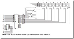
Figure 11–21 shows the 82C55 connected to a set of eight seven-segment LED displays. These are standard LEDs, but the interface can be modified with a change in resistor values for an organic LED (OLED) display or high-brightness LEDs. In this circuit, both ports A and B are programmed as (mode 0) simple latched output ports. Port A provides the segment data inputs to the display and port B provides a means of selecting one display position at a time for multiplexing the displays. The 82C55 is interfaced to an 8088 microprocessor through a PLD so that it functions at I/O port numbers 0700H–0703H. The program for the PLD is listed in Example 11–8. The PLD decodes the I/O address and develops the write strobe for the WR pin of the 82C55.
The resistor values are chosen in Figure 11–21 so that the segment current is 80 mA. This current is required to produce an average current of 10 mA per segment as the displays are multiplexed. A six-digit display uses a segment current of 60 mA for an average of 10 mA per segment. In this type of display system, only one of the eight display positions is on at any given instant. The peak anode current in an eight-digit display is 560 mA (seven segments × 80 mA), but the average anode current is 80 mA. In a six-digit display, the peak current would be 420 mA (seven segments × 60 mA). Whenever displays are multiplexed, we increase the segment current from 10 mA (for a display that uses 10 mA per segment as the nominal current) to a value equal to the number of display positions times 10 mA. This means that a four-digit display uses 40 mA per segment, a five-digit display uses 50 mA, and so on.
In this display, the segment load resistor passes 80 mA of current and has a voltage of approximately 3.0 V across it. The LED (1.65 V nominally) and a few tenths are dropped across the anode switch and the segment switch, hence a voltage of 3.0 V appears across the segment load resistor. The value of the resistor is 3.0 V ÷ 180 mA = 37.5 Ω. The closest standard resistor value of 39 Ω is used in Figure 11–21 for the segment load.
The resistor in series with the base of the segment switch assumes that the minimum gain of the transistor is 100. The base current is therefore 80 mA ÷ 100 = 0.8 mA. The voltage across the base resistor is approximately 3.0 V (the minimum logic 1 voltage level of the 82C55), minus the drop across the emitter-base junction (0.7 V), or 2.3 V. The value of the base resistor is there- fore 2.3 V ÷ 0.8mA = 2.875 KΩ. The closest standard resistor value is 2.7 KΩ, but 2.2 KΩ is chosen for this circuit.
The anode switch has a single resistor on its base. The current through the resistor is 560 mA ÷ 100 = 5.6 mA because the minimum gain of the transistor is 100. This exceeds the
maximum current of 4.0 mA from the 82C55, but this is close enough so that it will work with- out problems. The maximum current assumes that you are using the port pin as a TIL input to another circuit. If the amount of current were over 8.0–10.0 mA, then appropriate circuitry (in the form of either a Darlington-pair or another transistor switch) would be required. Here, the voltage across the base resistor is 5.0 V, minus the drop across the emitter-base junction (0.7 V), minus the voltage at the port pin (0.4 V), for a logic 0 level. The value of the resistor is 3.9 V ÷ 5.66 mA = 68.9 Ω. The closest standard resistor value is 69 Ω, which is chosen for this example.
Before software to operate the display is examined, we must first program the 82C55. This is accomplished with the short sequence of instructions listed in Example 11–9. Here, ports A and B are both programmed as outputs.
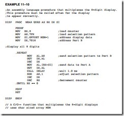
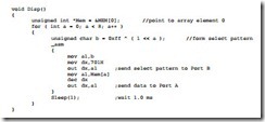
The procedure to multiplex the displays is listed in Example 11–10 in both assembly language and C++ with assembly language. For the display system to function correctly, we must call this procedure often. Notice that the procedure calls another procedure (DELAY) that causes a 1.0 ms time delay. The time delay is not illustrated in this example, but it is used to allow time for each display position to turn on. Manufacturers of LED displays recommend that the display flashes between 100 and 1500 times per second. Using a 1.0 ms time delay, each digit is displayed for 1.0 ms for a total display flash rate of 1000 Hz ÷ 8 or a flash rate of 125 Hz for all eight digits.
The display procedure (DISP) addresses an area of memory where the data, in seven- segment code, are stored for the eight display digits called MEM. The AH register is loaded with a code (7FH) that initially addresses the most significant display position. Once this position is selected, the contents of memory location MEM +7 is addressed and sent to the most significant digit. The selection code is then adjusted to select the next display digit. This process repeats eight times to display the contents of location MEM through MEM +7 on the eight display digits.
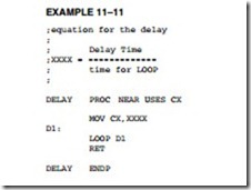
The time delay of 1.0 ms can be obtained by writing a procedure that uses the system clock frequency to determine how long each instruction requires to execute. The procedure listed in Example 11–11 causes a time delay of a duration determined by the number of times that the LOOP instruction executes. Here XXXX was used and will be filled in with a value after a few facts are discussed. The LOOP instruction requires a certain number of clocks to execute—how many can be located in Appendix B. Suppose that the interface is using the 80486 microprocessor running with a 20 MHz clock. Appendix B represents that the LOOP instruction requires 7/6 clocks. The first number is the number of clocks required when a jump to D1 occurs and the second number is when the jump does not occur. With a 20 MHz clock, one clock requires
1 ÷ 20 MHz = 50 ns. The LOOP instruction, in this case, requires 350 ns to execute in all but the very last iteration. To determine the count (XXXX) needed to accomplish a 1.0 ms time delay, divide 1.0 ms by 350 ns. In this case XXXX = 2,857 to accomplish a 1.0 ms time delay. If a larger count occurs, a LOOPD instruction can be used with the ECX register. The time required to execute the MOV CX, XXXX, and RET instructions can usually be ignored.
Suppose a Core2 with a 2.0 GHz clock is used for the delay. Here one clock is 0.5 ns and LOOP requires five clocks per iteration. This requires a count of 400,000, so LOOPD would be used with ECX.
If the program is written for the Windows environment, such as for use in an embedded system using embedded Windows, time delays can use a timer. The timer can operate with a pre- cision of milliseconds, and in the embedded version of Windows, the delays are guaranteed.
An LCD Display Interfaced to the 82C55
LCDs (liquid crystal displays) have replaced LED displays in many applications. The only disadvantage of the LED display is that it is difficult to see in low-light situations in which the LED is still in limited use. An example is medical equipment for older people with poor eyesight. If the price of the OLED becomes low enough, LCD displays will disappear. A German company currently manufactures an OLED display panel that sells for under $10.
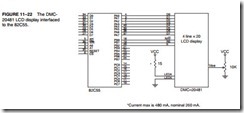
Figure 11–22 illustrates the connection of the Optrex DMC-20481 LCD display interfaced to an 82C55. The DMC-20481 is a 4-line by 20-characters-per-line display that accepts ASCII code as input data. It also accepts commands that initialize it and control its application. As you can see in Figure 11–22, the LCD display has few connections. The data connections, which are attached to the 82C55 port A, are used to input display data and to read information from the dis- play. This illustrates an 8-bit interface. If a 4-bit interface is desired, D4–D7 pins are used for the data where the data must be formatted with the high nibble first, followed by the low nibble.
A few newer OLED devices also contain a serial interface that uses a single pin for the data.
There are four control pins on the display. The VEE connection is used to adjust the contrast of the LED display and is normally connected to a 10 KQ potentiometer, as illustrated. The RS (register select) input selects data (RS = 1) or instructions (RS = 0). The E (enable) input must be a logic 1 for the DMC-20481 to read or write information and functions as a clock. Finally, the R/W pin selects a read or a write operation. Normally, the RS pin is placed at a 1 or 0, the R/W pin is set or cleared, data are placed on the data input pins, and then the E pin is pulsed to access the DMC-20481. This display also has two inputs (LEDA [anode] and LEDK [cathode]) for back-lighting LED diodes, which are not shown in the illustration.
In order to program the DMC-20481 we must first initialize it. This applies to any display that uses the HD44780 (Hitachi) display driver integrated circuit. The entire line of small display panels from Optrex and most other manufacturers is programmed in the same manner. Initialization is accomplished via the following steps:
1. Wait at least 15 ms after VCC rises to 5.0 V.
2. Output the function set command (30H), and wait at least 4.1 ms.
3. Output the function set command (30H) a second time, and wait at least 100 μs.
4. Output the function set command (30H) a third time, and wait at least 40 μs.
5. Output the function set command (38H) a fourth time, and wait at least 40 μs.
6. Output 08H to disable the display, and wait at least 40 μs.
7. Output a 01H to home the cursor and clear the display, and wait at least 1.64 ms.
8. Output the enable display cursor off (0CH), and wait at least 40 μs.
9. Output 06H to select auto-increment, shift the cursor, and wait at least 40 μs.
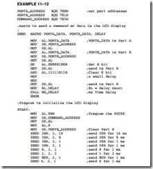
The software to accomplish the initialization of the LCD display is listed in Example 11–12. It is long, but the display controller requires the long initialization dialog. Note that the software for the three time delays is not included in the listing. If you are interfacing to a PC, you can use the RDTSC instruction as discussed in the Pentium chapter for the time delay. If you are developing the interface for another application, then you must write separate time delays, which must provide the delay times indicated in the initialization dialog. The time delays can also be obtained by using a timer in C++.
The NOP instructions are added in the SEND macro to ensure that the E bit remains a logic 1 long enough to activate the LCD display. This process should work in most systems at most clock frequencies, but additional NOP instructions may be needed to lengthen this time in some cases. Also notice that equate statements are used to equate the port addresses to labels. This is done so that the software can be changed easily if the port numbers differ from those used in the program.
Before programming the display, the commands used in the initialization dialog must be explained. See Table 11–3 for a complete listing of the commands or instructions for the LCD dis- play. Compare the commands sent to the LCD display in the initialization program to Table 11–3.
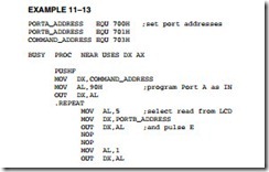
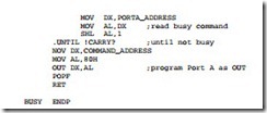
Once the LCD display is initialized, a few procedures are needed to display information and control the display. After initialization, time delays are no longer needed when sending data or many commands to the display. The clear display command still needs a time delay because the busy flag is not used with that command. Instead of a time delay, the busy flag is tested to see whether the display has completed an operation. A procedure to test the busy flag appears in Example 11–13. The BUSY procedure tests the LCD display and only returns when the display has completed a prior instruction.
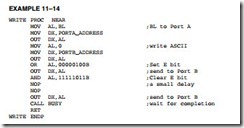
Once the BUSY procedure is available, data can be sent to the display by writing another procedure called WRITE. The WRITE procedure uses BUSY to test before trying to write new data to the display. Example 11–14 shows the WRITE procedure, which transfers the ASCII character from the BL register to the current cursor position of the display. Note that the initialization dialog has sent the cursor for auto-increment, so if WRITE is called more than once, the characters writ- ten to the display will appear one next to the other, as they would on a video display.
The only other procedure that is needed for a basic display is the clear and home cursor procedure, called CLS, shown in Example 11–15. This procedure uses the SEND macro from the initialization software to send the clear command to the display. With CLS and the procedures presented thus far, you can display any message on the display, clear it, display another message, and basically operate the display. As mentioned earlier, the clear command requires a time delay (at least 1.64 ms) instead of a call to BUSY for proper operation.
Additional procedures that could be developed might select a display RAM position. The display RAM address starts at 0 and progresses across the display until the last character address on the first line is location 19, location 20 is the first display position of the second line, and so forth. Once you can move the display address, you can change individual characters on the display and even read data from the display. These procedures are for you to develop if they are needed.
A word about the display RAM inside of the LCD display. The LCD contains 128 bytes of memory, addressed from 00H to 7FH. Not all of this memory is always used. For example, the ne-line × 20-character display uses only the first 20 bytes of memory (00–13H.) The first line of any of these displays always starts at address 00H. The second line of any display powered by the HD44780 always begins at address 40H. For example, a two-line × 40-character display uses addresses 00H–27H to store ASCII-coded data from the first line. The second line is stored at addresses 40H–67H for this display. In the four-line displays, the first line is at 00H, the second is at 40H, the third is at 14H, and the last line is at 54H. The largest display device that uses the HD44780 is a two-line × 40-character display. The four-line by 40-character display uses an M50530 or a pair of HD44780s. Because information on these devices can be readily found on the Internet, they are not covered in the text.
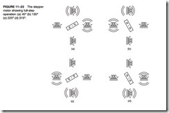
A Stepper Motor Interlaced to the 82C55. Another device often interfaced to a computer sys- tem is the stepper motor. A stepper motor is a digital motor because it is moved in discrete steps as it traverses through 360°. A common stepper motor is geared to move perhaps 15° per step in an inexpensive stepper motor, to 1° per step in a more costly, high-precision stepper motor. In all cases, these steps are gained through many magnetic poles and/or gearing. Notice that two coils are energized in Figure 11–23. If less power is required, one coil may be energized at a time, causing the motor to step at 45°, 135°, 225°, and 315°.
Figure 11–23 shows a four-coil stepper motor that uses an armature with a single pole. Notice that the stepper motor is shown four times with the armature (permanent magnetic) rotated to four discrete places. This is accomplished by energizing the coils, as shown. This is an illustration of full stepping. The stepper motor is driven by using NPN Darlington amplifier pairs to provide a large current to each coil.
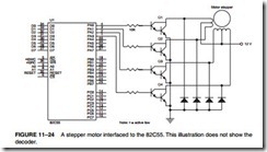
A circuit that can drive this stepper motor is illustrated in Figure 11–24, with the four coils shown in place. This circuit uses the 82C55 to provide it with the drive signals that are used to rotate the armature of the motor in either the right-hand or left-hand direction.
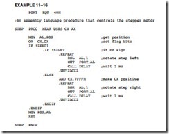
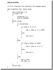
A simple procedure that drives the motor (assuming that port A is programmed in mode 0 as an output device) is listed in Example 11–16 in both assembly language and as a function in C++. This subroutine is called, with CX holding the number of steps and direction of the rotation. If CX is greater than 8000H, the motor spins in the right-hand direction; if CX is less than 8000H, it spins in the left-hand direction. For example, if the number of steps is 0003H, the motor moves in the left-hand direction three steps and if the number of steps is 8003H, it moves three steps in the right- hand direction. The leftmost bit of CX is removed and the remaining 15 bits contain the number of steps. Notice that the procedure uses a time delay (not illustrated) that causes a l ms time delay. This time delay is required to allow the stepper-motor armature time to move to its next position.
The current position is stored in memory location POS, which must be initialized with 33H, 66H, 0EEH, or 99H. This allows a simple ROR (step right) or ROL (step left) instruction to rotate the binary bit pattern for the next step.
The C++ version has two parameters: Pos is the current position of the stepper motor and Step is the number of steps as described earlier. The new Pos is returned in the C++ version instead of being stored in a variable.
Stepper motors can also be operated in the half-step mode, which allows eight steps per sequence. This is accomplished by using the full-step sequence described with a half step obtained by energizing one coil interspersed between the full steps. Half-stepping allows the armature to be positioned at 0°, 90°, 180°, and 270°. The half-step position codes are 11H, 22H, 44H, and 88H. A complete sequence of eight steps would be as follows: 11H, 33H, 22H, 66H, 44H, 0CCH, 88H, and 99H. This sequence could be either output from a lookup table or generated with software.
Key Matrix Interface. Keyboards come in a vast variety of sizes, from the standard 101-key QWERTY keyboards interfaced to the microprocessor to small specialized keyboards that may contain only four to 16 keys. This section of the text concentrates on the smaller keyboards that may be purchased preassembled or may be constructed from individual key switches.
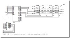
Figure 11–25 illustrates a small key-matrix that contains 16 switches interfaced to ports A and B of an 82C55. In this example, the switches are formed into a 4 × 4 matrix, but any matrix could be used, such as a 2 × 8. Notice how the keys are organized into four rows (ROW0–ROW3)
and four columns (COL0–COL3). Each row is connected to 5.0 V through a 10 KΩ pull-up resistor to ensure that the row is pulled high when no push-button switch is closed.
The 82C55 is decoded (the PLD program is not shown) at I/O ports 50H–53H for an 8088 microprocessor. Port A is programmed as an input port to read the rows and port B is programmed as an output port to select a column. For example, if 1110 is output to port B pins PB3–PB0, column 0 has a logic 1, so the four keys in column 0 are selected. Notice that with a logic 0 on PB0, the only switches that can place a logic 0 onto port A are switches 0–3. If switches 4–F are closed, the corresponding port A pins remain a logic 1. Likewise, if 1101 is output to port B, switches 4–7 are selected, and so forth.
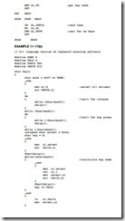
A flowchart of the software required to read a key from the keyboard matrix and debounce the key is illustrated in Figure 11–26. Keys must be debounced, which is normally accomplished with a short time delay of 10–20 ms. The flowchart contains three main sections. The first waits for the release of a key. This seems awkward, but software executes very quickly in a micro- processor and there is a possibility that the program will return to the top of this program before
the key is released, so we must wait for a release first. Next, the flowchart shows that we wait for a keystroke. Once the keystroke is detected, the position of the key is calculated in the final part of the flowchart.
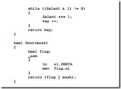
The software uses a procedure called SCAN to scan the keys and another called DELAY10 (not shown in this example) to waste 10 ms of time for debouncing. The main keyboard proce- dure is called KEY and it appears with the others in Example 11–17. Example 11–17 also lists a C++ function to accomplish a key read operation. Note that the KEY procedure is generic, so it can handle any keyboard configuration from a 1 × 1 matrix to an 8 × 8 matrix. Changing the two equates at the start of the program (ROWS and COLS) will change the configuration of the soft- ware for any size keyboard. Also note that the steps required to initialize the 82C55 so that port A is an input port and port B is an output port are not shown.
With certain keyboards that do not follow the way keys are scanned, a lookup table may be needed to convert the raw key codes returned by KEY into key codes that match the keys on the keyboard. The lookup software is placed just before returning from KEY. It is merely a MOV BX,OFFSET TABLE followed by the XLAT instruction.
The ShortDelay procedure is needed because the computer changes port B at a very high rate of speed. The short time delay allows time for the data sent to port B to settle to their final state. In most cases, this is not needed if the scan rate (time between output instructions) of this part of the software does not exceed 30 KHz. If the scanning frequency is higher, the device generates radio interference. If it does, the Federal Communications Commission (FCC) will not approve its application in any accepted system. Without FCC Type A or Type B certification the system cannot be sold.
Mode 1 Strobed Input
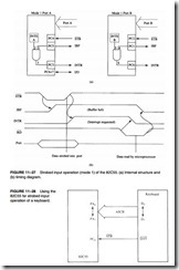
Mode 1 operation causes port A and/or port B to function as latching input devices. This allows external data to be stored into the port until the microprocessor is ready to retrieve it. Port C is also used in mode 1 operation—not for data, but for control or handshaking signals that help operate either or both port A and port B as strobed input ports. Figure 11–27 shows how both ports are structured for mode 1 strobed input operation and the timing diagram.
The strobed input port captures data from the port pins when the strobe (STB) is activated. Note that the strobe captures the port data on the 0-to-1 transition. The STB signal causes data to be captured in the port, and it activates the IBF (input buffer full) and INTR (interrupt request) sig- nals. Once the microprocessor, through software (IBF) or hardware (INTR), notices that data are strobed into the port, it executes an IN instruction to read the port RD. The act of reading the port restores both IBF and INTR to their inactive states until the next datum is strobed into the port.
 Signal Definitions for Mode 1 Strobed Input
STB
The strobe input loads data into the port latch, which holds the information until it is input to the microprocessor via the IN instruction.
IBF Input buffer full is an output indicating that the input latch contains information.
![]() INTR Interrupt request is an output that requests an interrupt. The INTR pin becomes a logic 1 when the STB input returns to a logic 1, and is cleared when the data are input from the port by the microprocessor.
INTR Interrupt request is an output that requests an interrupt. The INTR pin becomes a logic 1 when the STB input returns to a logic 1, and is cleared when the data are input from the port by the microprocessor.
INTE The interrupt enable signal is neither an input nor an output; it is an internal bit programmed via the port PC4 (port A) or PC2 (port B) bit position.
PC7, PC6 The port C pins 7 and 6 are general-purpose I/O pins that are available for any purpose.
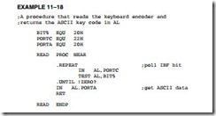
Strobed Input Example. An excellent example of a strobed input device is a keyboard. The keyboard encoder debounces the key switches and provides a strobe signal whenever a key is
depressed and the data output contain the ASCII-coded key code. Figure 11–28 illustrates a key- board connected to strobed input port A. Here DAV (data available) is activated for 1.0 μs each time that a key is typed on the keyboard. This causes data to be strobed into port A because DAV is connected to the STB input of port A. Each time a key is typed, therefore, it is stored into port A of the 82C55. The STB input also activates the IBF signal, indicating that data are in port A.
Example 11–17 shows a procedure that reads data from the keyboard each time a key is typed. This procedure reads the key from port A and returns with the ASCII code in AL. To detect a key, port C is read and the IBF bit (bit position PC5) is tested to see whether the buffer is full. If the buffer is empty (IBF = 0), then the procedure keeps testing this bit, waiting for a character to be typed on the keyboard.
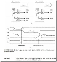
Mode 1 Strobed Output
Figure 11–29 illustrates the internal configuration and timing diagram of the 82C55 when it is operated as a strobed output device under mode 1. Strobed output operation is similar to mode 0 output operation, except that control signals are included to provide handshaking.
Whenever data are written to a port programmed as a strobed output port, the OBF (output buffer full) signal becomes a logic 0 to indicate that data are present in the port latch. This sig- nal indicates that data are available to an external I/O device that removes the data by strobing the ACK (acknowledge) input to the port. The ACK signal returns the OBF signal to a logic 1, indicating that the buffer is not full.
Signal Definitions for Mode 1 Strobed Output
OBF
ACK
Output buffer full is an output that goes low whenever data are output (OUT) to the port A or port B latch. This signal is set to a logic 1 whenever the ACK pulse returns from the external device.
The acknowledge signal causes the OBF pin to return to a logic 1 level. The ACK signal is a response from an external device, indicating that it has received the data from the 82C55 port.
INTR Interrupt request is a signal that often interrupts the microprocessor when the external device receives the data via the ACK signal. This pin is qualified by the internal INTE (interrupt enable) bit.
INTE Interrupt enable is neither an input nor an output; it is an internal bit programmed to enable or disable the INTR pin. The INTE A bit is programmed using the PC6 bit and INTE B is programmed using the PC2 bit.
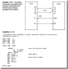
Strobed Output Example. The printer interface discussed in Section 11–1 is used here to demonstrate how to achieve strobed output synchronization between the printer and the 82C55. Figure 11–30 illustrates port B connected to a parallel printer, with eight data inputs for receiving ASCII-coded data, a DS (data strobe) input to strobe data into the printer, and an ACK out- put to acknowledge the receipt of the ASCII character.
In this circuit, there is no signal to generate the DS signal to the printer, so PC4 is used with software that generates the DS signal. The ACK signal that is returned from the printer acknowledges the receipt of the data and is connected to the ACK input of the 82C55.
Example 11–19 lists the software that sends the ASCII-coded character in AH to the printer. The procedure first tests OBF to decide whether the printer has removed the data from port B. If not, the procedure waits for the ACK signal to return from the printer. If OBF = 1, then the procedure sends the contents of AH to the printer through port B and also sends the DS signal.
Mode 2 Bidirectional Operation
In mode 2, which is allowed with group A only, port A becomes bidirectional, allowing data to be transmitted and received over the same eight wires. Bidirectional bused data are useful when interfacing two computers. It is also used for the IEEE-488 parallel high-speed GPIB (general- purpose instrumentation bus) interface standard. Figure 11–31 shows the internal structure and timing diagram for mode 2 bidirectional operation.
Signal Definitions for Bidirectional Mode 2
INTR Interrupt request is an output used to interrupt the microprocessor for both input and output conditions.
OBF ACK
Output buffer full is an output indicating that the output buffer contains data for the bidirectional bus.
Acknowledge is an input that enables the three-state buffers so that data can appear on port A. If ACK is a logic 1, the output buffers of port A are at their high-impedance state.
STB
The strobe input loads the port A input latch with external data from the bidirectional port A bus.
IBF Input buffer full is an output used to signal that the input buffer contains data for the external bidirectional bus.
INTE Interrupt enable are internal bits (INTE1 and INTE2) that enable the INTR pin. The state of the INTR pin is controlled through port C bits PC6 (INTE1) and PC4 (INTE2).
PC0, PC1, and PC2 These pins are general-purpose I/O pins in mode 2 controlled by the bit set and reset command.
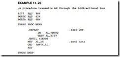
The Bidirectional Bus. The bidirectional bus is used by referencing port A with the IN and OUT instructions. To transmit data through the bidirectional bus, the program first tests the OBF signal to determine whether the output buffer is empty. If it is, then data are sent to the output buffer via the OUT instruction. The external circuitry also monitors the OBF signal to decide whether the microprocessor has sent data to the bus. As soon as the output circuitry sees a logic 0 on OBF, it sends back the ACK signal to remove it from the output buffer. The ACK signal sets the OBF bit and enables the three-state output buffers so that data may be read. Example 11–20 lists a procedure that transmits the contents of the AH register through bidirectional port A.
To receive data through the bidirectional port A bus, the IBF bit is tested with software to decide whether data have been strobed into the port. If IBF = 1, then data is input using the IN instruction. The external interface sends data into the port by using the STB signal. When STB is activated, the IBF signal becomes a logic 1 and the data at port A are held inside the port in a latch. When the IN instruction executes, the IBF bit is cleared and the data in the port are moved into AL. Example 11–21 lists a procedure that reads data from the port.
The INTR (interrupt request) pin can be activated from both directions of data flow through the bus. If INTR is enabled by both INTE bits, then the output and input buffers both cause interrupt requests. This occurs when data are strobed into the buffer using STB or when data are written using OUT.
82C55 Mode Summary
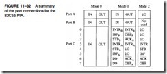
Figure 11–32 shows a graphical summary of the three modes of operation for the 82C55. Mode 0 provides simple I/O, mode 1 provides strobed I/O, and mode 2 provides bidirectional I/O. As mentioned, these modes are selected through the command register of the 82C55.
The Serial EEPROM Interface
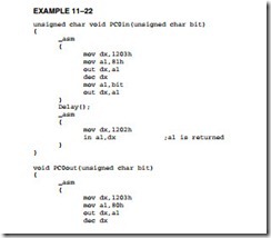
In Chapter 10, Figure 10–23, a serial EEPROM is illustrated, but at that point in the text, no I/O existed for an interface. Suppose that port C of an 82C55 is used for connection to this interface and software is needed to drive the interface. It is assumed that pin PC4 connects to the SCL input and pin PC0 connects to the serial connection (SDA). PC4 is programmed as an output pin to provide a clock signal. The PC0 pin is programmed as an output to send data and as an input to receive data from the EEPROM.
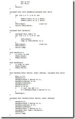
Refer to Figure 10–24; the data format for the software for reading and writing data to the EEPROM is also illustrated in Example 11–22. This software is written in C with some assembly language, but it can also be developed in assembly language. The I/O port addresses are 0x1203 for the command register and 0x1202 for the port C register. The time delay should be μs for a data rate of 400 KHz. Note that the time delay software is not illustrated here and the while loop is used to wait for an ACK signal after a write.
