16550 PROGRAMMABLE COMMUNICATIONS INTERFACE
The National Semiconductor Corporation’s PC16550D is a programmable communications inter- face designed to connect to virtually any type of serial interface. The 16550 is a universal asynchronous receiver/transmitter (UART) that is fully compatible with the Intel microprocessors. The 16550 is capable of operating at 0–1.5 M baud. Baud rate is the number of bits transferred per second (bps), including start, stop, data, and parity (Bps is bytes per second and bps are bits per second). The 16550 also includes a programmable baud rate generator and separate FIFOs for input and output data to ease the load on the microprocessor. Each FIFO contains 16 bytes of storage. This is the most common communications interface found in modem microprocessor-based equipment, including the personal computer and many modems.
Asynchronous Serial Data
Asynchronous serial data are transmitted and received without a clock or timing signal. Figure 11–42 illustrates two frames of asynchronous serial data. Each frame contains a start bit, seven data bits, parity, and one stop bit. The figure shows a frame that contains one ASCII char- acter and 10 bits. Most dial-up communications systems of the past, such as CompuServe, Prodigy, and America Online, used 10 bits for asynchronous serial data with even parity. Most Internet and bulletin board services also use 10 bits, but they normally do not use parity. Instead, eight data bits are transferred, replacing parity with a data bit. This makes byte transfers of non- ASCII data much easier to accomplish.
16550 Functional Description
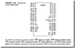
Figure 11–43 illustrates the pin-out of the 16550 UART. This device is available as a 40-pin DIP (dual in-line package) or as a 44-pin PLCC (plastic leadless chip carrier). Two completely separate sections are responsible for data communications: the receiver and the transmitter. Because each of these sections is independent, the 16550 is able to function in simplex, half- duplex, or full-duplex modes. One of the main features of the 16550 is its internal receiver and transmitter FIFO (first-in, first-out) memories. Because each is 16 bytes deep, the UART requires attention only from the microprocessor after receiving 16 bytes of data. It also holds 16 bytes before the microprocessor must wait for the transmitter. The FIFO makes this UART ideal when interfacing to high-speed systems because less time is required to service it.
An example simplex system is one in which the transmitter or receiver is used by itself such as in an FM (frequency modulation) radio station. An example half-duplex system is a CB (citizens band) radio, on which we transmit and receive, but not both at the same time. The full-duplex system allows transmission and reception in both directions simultaneously. An example of a full-duplex system is the telephone.
The 16550 can control a modem (modulator/demodulator), which is a device that converts TTL levels of serial data into audio tones that can pass through the telephone system. Six pins on
the 16650 are devoted to modem control: DSR (data set ready), DTR (data terminal ready), CTS (clear-to-send), RTS (request-to-send), RI (ring indicator), and DCD (data carrier detect). The modem is referred to as the data set and the 16550 is referred to as the data terminal.
16550 Pin Functions
A0, A1, A2 The address inputs are used to select an internal register for programming and also data transfer. See Table 11–5 for a list of each combination of the address inputs and the registers selected.
ADS
BAUDOUT
CS0, CS1, CS2 CTS
The address strobe input is used to latch the address lines and chip select lines. If not needed (as in the Intel system), connect this pin to ground. The ADS pin is designed for use with Motorola microprocessors.
The baud out pin is where the clock signal generated by the baud rate generator from the transmitter section is made available. It is most often connected to the RCLK input to generate a receiver clock that is equal to the transmitter clock.
The chip select inputs must all be active to enable the 16550 UART.
The clear-to-send (if low) indicates that the modem or data set is ready to exchange information. This pin is often used in a half-duplex system to turn the line around.
D0–D7 The data bus pins are connected to the microprocessor data bus.
DCD
The data carrier detect input is used by the modem to signal the 16550 that a carrier is present.
DDIS The disable driver output becomes a logic 0 to indicate that the micro- processor is reading data from the UART. DDIS can be used to change the direction of data flow through a buffer.
DSR DTR
Data set ready is an input to the 16550, indicating that the modem or data set is ready to operate.
Data terminal ready is an output that indicates that the data terminal (16550) is ready to function.
INTR Interrupt request is an output to the microprocessor used to request an interrupt (INTR = 1) whenever the 16550 has a receiver error, it has received data, and the transmitter is empty.
MR Master reset initializes the 16550 and should be connected to the system RESET signal.
OUT1, OUT2
User-defined output pins that can provide signals to a modem or any other device as needed in a system.
RCLK Receiver clock is the clock input to the receiver section of the UART. This input is always 16 times the desired receiver baud rate.
RD, RD RI
RTS
Read inputs (either may be used) cause data to be read from the register specified by the address inputs to the UART.
The ring indicator input is placed at the logic 0 level by the modem to indicate that the telephone is ringing.
Request-to-send is a signal to the modem indicating that the UART wishes to send data.
SIN, SOUT These are the serial data pins. SIN accepts serial data and SOUT transmits serial data.
RXRDY TXRDY WR, WR
Receiver ready is a signal used to transfer received data via DMA tech- niques (see text).
Transmitter ready is a signal used to transfer transmitter data via DMA techniques (see text).
Write (either may be used) connects to the microprocessor write signal to transfer commands and data to the 16550.
XIN, XOUT These are the main clock connections. A crystal is connected across these pins to form a crystal oscillator, or XIN is connected to an external timing source.
Programming the 16550
Programming the 16550 is simple, although it may be slightly more involved when compared to some of the other programmable interfaces described in this chapter. Programming is a two-part process that includes the initialization dialog and operational dialog.
In the personal computer, which uses the 16550 or its programming equivalent, the I/O port addresses are decoded at 3F8H through 3FFH for COM port 0 and 2F8H through 2FFH for COM port 2. Although the examples in this section of the chapter are not written specifically for the personal computer, they can be adapted by changing the port numbers to control the COM ports on the PC.
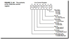
Initializing the 16550. Initialization dialog, which occurs after a hardware or software reset, consists of two parts: programming the line control register and the baud rate generator. The line control register selects the number of data bits, number of stop bits, and parity (whether it’s even or odd, or if parity is sent as a 1 or a 0). The baud rate generator is programmed with a divisor that determines the baud rate of the transmitter section.
Figure 11–44 illustrates the line control register. The line control register is programmed by outputting information to I/O port 011 (A2, A1, A0). The rightmost two bits of the line control register select the number of transmitted data bits (5, 6, 7, or 8). The number of stop bits is selected by S in the line control register. If S = 0, one stop bit is used; if S = 1, 1.5 stop bits are used for five data bits, and two stop bits are used with six, seven, or eight data bits.
The next three bits are used together to send even or odd parity, to send no parity, or to send a 1 or a 0 in the parity bit position. To send even or odd parity, the ST (stick) bit must be placed at a logic 0 level, and parity enable must be a logic 1. The value of the parity bit then determines even or odd parity. To send no parity (common in Internet connections), ST = 0 as well as the parity enable bit. This sends and receives data without parity. Finally, if a 1 or a 0 must be sent and received in the parity bit position for all data, ST = 1 with a 1 in parity enable. To send a 1 in the parity bit position, place a 0 in the parity bit; to send a 0, place a 1 in the parity bit. (See Table 11–6 for the operation of the parity and stick bits.)
The remaining bits in the line control register are used to send a break and to select programming for the baud rate divisor. If bit position 6 of the line control register is a logic 1, a break is transmitted. As long as this bit is a 1, the break is sent from the SOUT pin. A break, by definition, is at least two frames of logic 0 data. The software in the system is responsible for timing the transmission of the break. To end the break, bit position 6 or the line control register is returned to a logic 0 level. The baud rate divisor is only programmable when bit position 7 of the line control register is a logic 1.
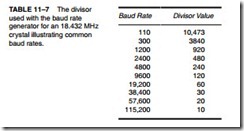
Programming the Baud Rate. The baud rate generator is programmed at I/O addresses 000 and 001 (A2, A1, A0). Port 000 is used to hold the least significant part of the 16-bit divisor and port 001 is used to hold the most significant part. The value used for the divisor depends on the external clock or crystal frequency. Table 11–7 illustrates common baud rates obtainable if an 18.432 MHz crystal is used as a timing source. It also shows the divisor values programmed into the baud rate generator to obtain these baud rates. The actual number programmed into the baud rate generator causes it to produce a clock that is 16 times the desired baud rate. For example, if 240 is programmed into the baud rate divisor, the baud rate is (18.432 MHz ÷ 16) × 240 = 4800 baud.
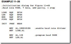
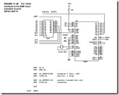
Sample Initialization. Suppose that an asynchronous system requires seven data bits, odd parity a baud rate of 9600, and one stop bit. Example 11–24 lists a procedure that initializes the 16550 to function in this manner. Figure 11–45 shows the interface to the 8088 microprocessor, using a PLD to decode the 8-bit port addresses F0H through F7H. (The PLD program is not shown.) Here port F3H accesses the line control register and F0H and F1H access the baud rate divisor registers. The last part of Example 11–26 is described with the function of the FIFO control register in the next few paragraphs.
After the line control register and baud rate divisor are programmed into the 16550, it is still not ready to function. After programming the line control register and baud rate, we still must program the FIFO control register, which is at port F2H in the circuit of Figure 11–45.
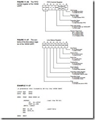
Figure 11–46 illustrates the FIFO control register for the 16550. This register enables the transmitter and receiver (bit 0 = 1), and clears the transmitter and receiver FIFOs. It also provides control for the 16550 interrupts, which are discussed in Chapter 12. Notice that the last section of Example 11–26 places a 7 into the FIFO control register. This enables the transmitter and receiver, and clears both FIFOs. The 16550 is now ready to operate, but without interrupts. Interrupts are automatically disabled when the MR (master reset) input is placed at a logic 1 by the system RESET signal.
Sending Serial Data. Before serial data can be sent or received through the 16550, we need to know the function of the line status register (see Figure 11–47). The line status register contains information about error conditions and the state of the transmitter and receiver. This register is tested before a byte is transmitted or can be received.
Suppose that a procedure (see Example 11–27) is written to transmit the contents of AH to the 16550 and out through its serial data pin (SOUT). The TH bit is polled by software to determine whether the transmitter is ready to receive data. This procedure uses the circuit of Figure 11–45.
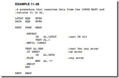
Receiving Serial Data. To read received information from the 16550, test the DR bit of the line status register. Example 11–28 lists a procedure that tests the DR bit to decide whether the 16550 has received any data. Upon the reception of data, the procedure tests for errors. If an error is detected, the procedure returns with AL equal to an ASCII ‘?’. If no error has occurred, then the procedure returns with AL equal to the received character.
UART Errors. The types of errors detected by the 16550 are parity error, framing error, and over- run error. A parity error indicates that the received data contain the wrong parity. A framing error indicates that the start and stop bits are not in their proper places. An overrun error indicates that data have overrun the internal receiver FIFO buffer. These errors should not occur during normal operation. If a parity error occurs, it indicates that noise was encountered during reception. A framing error occurs if the receiver is receiving data at an incorrect baud rate. An overrun error occurs only if the software fails to read the data from the UART before the receiver FIFO is full. This example does not test the BI (break indicator bit) for a break condition. Note that a break is two consecutive frames of logic 0s on the SIN pin of the UART. The remaining registers, which are used for interrupt control and modem control, are developed in Chapter 12.

