10.9 68000 Clock and Reset Signals
This section covers generation of 68000 clock and reset signals in detail because the clock signal and the reset pins are two important signals of any microprocessor.
10.9.1 68000 Clock Signals
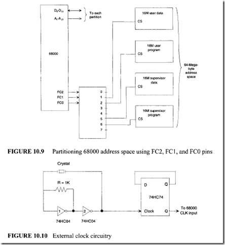
As mentioned before, the 68000 D0es not include an on-chip clock generation circuitry. This means that an external crystal oscillator chip is required to generate the clock. The 68000 CLK input can be provided by a crystal oscillator or by designing an external circuit. Figure 10.10 shows a simple oscillator to generate the 68000 CLK input.
This circuit uses two inverters connected in series. Inverter 1 is biased in its
transition region by the resistor R. Inverter I inputs the crystal output (sinusoidal) to provide a logic pulse train at the output of inverter 1. Inverter 2 sharpens the wave and drives the crystal. For this circuit to work, HCMOS logic for the inverters must be used. Therefore, the 74HC04 inverter chip is used. The 74HC04 has high noise immunity and the ability to drive I 0 LS-TTL loads. A coupling capacitor should be connected across the supply terminals to reduce the ringing effect during high-frequency switching of the HCMOS devices. Note that the ringing occurs when a circuit oscillates for a short time due to the presence of stray inductance and capacitance. In addition, the output of this oscillator is fed to the CLK input of a D flip-flop (74HC74) to further reduce the ringing. A clo k signal of 50% duty cycle at a frequency ofY2 the crystal frequency is generated. This means that this circuit with a 16-MHz crystal will generate an 8-MHz clock for the 68000.
10.9.2 68000 Reset Circuit
When designing the microprocessor’s reset circuit, two types of reset must be considered: power-up and manual. These reset circuits must be designed using the parameters specified by the manufacturer. Therefore, a microprocessor must be reset when its Vee pin is connected to power. This is called "power-up reset." After some time during normal operation, the microprocessor can be reset by the designer upon activation of a manual switch such as a pushbutton. A reset circuit, therefore, needs to be designed following the timing parameters associated typically with the microprocessor’s reset input pin specified by the manufacturer. The reset circuit, once designed, is typically connected to the microprocessor’s reset pin.
Upon hardware reset, the 68000 sets the S-bit in SR to 1 and performs the following:
1. The 68000 loads the supervisor stack pointer from addresses $000000 (high 16 bits) and $000002 (low 16 bits) and loads the PC from $000004 (high 16 bits) and $000006 (low 16 bits). Typical 68000 assembler directives such as DC.L can be used for this purpose. For example, to load $200128 into supervisor SP and $3Fl420 into PC, the following instruction sequence can be used:
 2. The 68000 clears the trace bit in SR to 0 and sets the interrupt mask bits 12 I 1 IO in SR to 111. All other registers are unaffected.
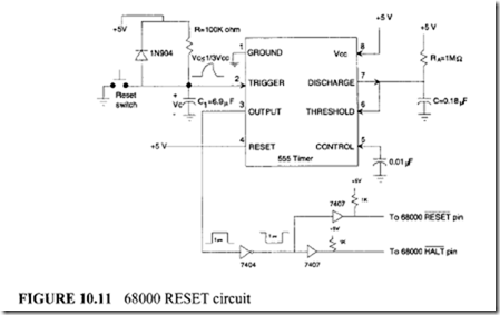
To cause a power-up reset, Motorola specifies that both the RESET and HALT pins of the 68000 must be held LOW for at least 100 ms. This means that an external circuit needs to be designed that will generate a negative pulse with a width of at least 100 ms for both RESET and HALT. The manual RESET requires both the RESET and HALT pins to be LOW for at least 10 cycles( 1.25 microseconds for 8MHz). In general, it is safer to assert RESET and HALT for much longer than the minimum requirements. Figure 10.11 shows a typical 68000 reset circuit that asserts RESET and HALT LOW for approximately 200 ms. The 555 timer is used in the circuit.
The reset circuit in the figure utilizes the 555 timer chip and provides for both power-up and manual resets by asserting the 68000 RESET and HALT pins for at least 200 ms. The computer designer D0es not have to know about the details of the 555 chip. Instead, the designer should know how to use the 555 chip to generate the 68000 RESET signal.
The 555 is a linear 8-pin chip. The TRIGGER pin is the input signal. When the voltage at the TRIGGER input pin is less than or equal to 1/3 Vw the OUTPUT pin is HIGH. The DISCHARGE and THRESHOLD pins are tied together to RA and C. Note that the values of RA and C determine the output pulse width. The CONTROL input pin controls the THRESHOLD input voltage. According to the manufacturer’s data sheets, the control input should be connected to a 0.01-flF capacitor whose other lead should be grounded. Also, from the manufacturer’s data sheets, the output pulse width, tpw = 1.1 RAC seconds. The values of RA and C can be chosen for stretching out the pulse width. An RC circuit is connected at the 555 TRIGGER pin. A slow pulse obtained by charging and discharging the capacitor C1 is applied at the 555 TRIGGER input pin. The 555 will generate a clean and fast pulse at the output. Capacitor C1 is at zero voltage upon power-up. This is obviously lower than 1/3 Vee with Vee= 5 V. Thus, the 555 will generate a HIGH at the OUTPUT pin. The OUTPUT pin is connected through a 7404 inverter to provide a LOW at the 68000 RESET and HALT pins. The 7404 output is buffered via two 7407’s (noninverting buffers) to ensure adequate currents for the 68000 RESET and HALT pins. Note that the 7407 provides an open collector output. Therefore, a 1-Kohm pull-up is used
for each 7407. Now, let us explain how the timing requirements for the 68000 RESET are satisfied.
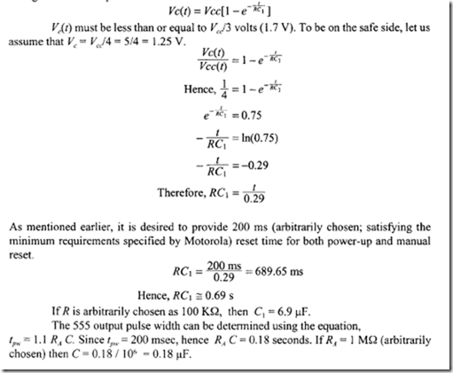
As mentioned before, capacitor C1 is initially at zero voltage upon power-up. C1 then charges to vee after a definite time determined by the time constant, RCI. The charging
voltage across the capacitor is
The reverse-biased diode (IN904 or equivalent) connected at the 555 TRIGGER input circuit is used to hold the capacitor (C1 charged to 1.25 V) voltage at 1.25 V in case Vee (obtained using a power supply from AC voltage) drops below 5V to a level such that the capacitor C1 may discharge through the 100-KQ resistor. In such a situation, the diode will be forward biased essentially shorting out the 100-Kohm resistor, thus maintaining the capacitor voltage at 1.25 V.
In Figure 10.11, upon power-up, the capacitor C1 charges to approximately 1.25 V. After some time, if the reset switch is depressed, the capacitor is short-circuited to ground. The capacitor, therefore, discharges to zero. This logic 0 at the 555 TRIGGER input pin will provide 200 ms LOW at the 68000 RESET and HALT input pins. This will satisfy the minimum requirement of 10 clock cycles( 1.25 microseconds for 8MHz clock) at the 68000 RESET and HALT pins for manual reset. The values of R and C1 at the 555 trigger input should be recalculated for other 68000 clock frequencies for manual reset Note that the 68000 power-up reset time is fixed with a timing requirement of at least 100 ms whereas the manual reset time depends on the 68000 clock frequency and must be at least 10 clock cycles.
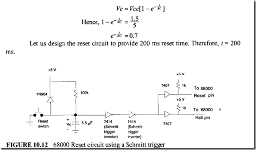
Another way of generating the power-up and manual resets is by using a Schmitt trigger inverter such as the 7414 chip. Figure 10.12 shows a typical circuit. The purpose of the Schmitt trigger in a microprocessor reset circuit has already been explained in Chapter 9 for 8086 reset using the 8284 chip. The operation of the 68000 power-up and manual resets using the RC circuit in Figure 10.12 has already been described in this section. The purpose of the two 7414 Schmitt-trigger inverters is primarily to shape up a slow pulse generated by the RC circuit to obtain a fast and clean negative pulse. Two 7407 open-collector noninverting buffers are used to amplify currents for the 68000 RESET and HALT pins. Let us now determine the values of R and C.
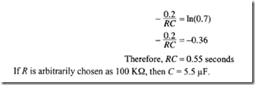
When the input of the 7414 Schmitt-trigger inverter is low (0 V for example), the output will be HIGH, typically at about 3.7 V. For input voltage from 0 to about 1.7 V, the output of the 7414 will be HIGH. Let us arbitrarily ch00se Ve = 1.5V to provide a low at the input of the first 7414 in the figure. As before,
10.10 68000 Read and Write Cycle Timing Diagrams
The 68000 family of processors (68000, 68008, 68010, and 68012) uses a handshaking mechanism to transfer data between the processors and peripheral devices. This means that all these processors can transfer data asynchronously to and from peripherals of varying speeds.
During the read cycle, the 68000 obtains data from a memory location or an I/O port. If the instruction specifies a word (such as MOVE .W $ 0 2 0 50 4 , D1) or a long word (such as MOVE .L $ 0 30 8 0 8 , D0), the 68000 reads both upper and lower bytes at the same time by asserting the UDS and LDS pins. When the instruction is for a byte operation, the 68000 utilizes an internal bit to find which byte to read and then outputs the data strobe required for that byte.
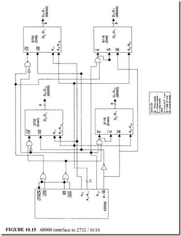
For byte operations, when the address is even (A0 = 0), the 68000 asserts UDS and reads data via the Ds-D 15 pins into the low byte of the specified data register. On the other hand, when the address is odd (A0 = 1), the 68000 outputs a LOW on LDS and reads data via the D0-D7 pins to the low byte of the specified data register. For example, consider MOVE. B $50 714 4, 05. The 68000 outputs a LOW on UDS (because A0 = 0) and a HIGH on LDS. The memory chip’s eight data lines must be connected to the 68000 Ds-D15 pins. The 68000 reads the data byte via the Ds-D15 pins into the low byte of D5. Note that, for reading a byte from an odd address, the data lines of the memory chip must be connected to the 68000 D0-D7 pins. In this case, the 68000 outputs a LOW on LDS (because A0 = 1) and a HIGH on UDS, and then reads the data byte into the low byte of the data register.
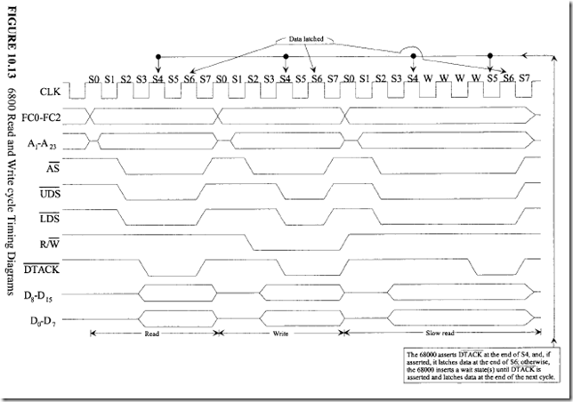
Figure I 0.13 shows the read/write timing diagrams. During SO, address and data signals are in the high-impedance state. At the start of Sl, the 68000 outputs the address on its address pins (A 1-A23 ). During SO, the 68000 outputs FC2-FCO signals. AS is asserted at the start of S2 to indicate a valid address on the bus. AS can be used at this point to latch the signals on the address pins. The 68000 asserts the UDS, LDS, and RIW = 1 to indicate a READ operation. The 68000 now waits for the peripheral device to assert DTACK. Upon placing data on the data bus, the peripheral device asserts DTACK. The 68000 samples the DTACK signal at the end of S4. If DTACK is not asserted by the peripheral device, the processor automatically inserts a wait state(s) (W).
However, upon assertion of DTACK, the 68000 negates the AS, UDS, and LDS signals, and latches the data from the data bus into an internal register at the end of the next cycle. Once the selected peripheral device senses that the 68000 has obtained data from the data bus (by recognizing the negation of AS, UDS, or LDS ), the peripheral device must negate DTACK immediately so that it D0es not interfere with the start of the next cycle.
If DTACK is not asserted by the peripheral at the end of S4 (Figure I 0.13, SLOW READ), the 68000 inserts wait states. The 68000 outputs valid addresses on the address pins and keeps asserting AS, UDS, and LDS until the peripheral asserts DTACK. The 68000 always inserts an even number of wait states if DTACK is not asserted by the peripheral because all 68000 operations are performed using the clock with two states per clock cycle. Note in Figure 10.13 that the 68000 inserts 4 wait states or 2 cycles.
As an example of word read, consider that the 68000 is ready to execute the MOVE .W $ 6 0 212 2 , D0 instruction. The 68000 performs as follows:
1. At the end of S0 the 68000 places the upper 23 bits of the address 602122 16 on A3-A23·
2. At the end of SI, the 68000 asserts AS, UDS, and LDS.
3. The 68000 continues to output a HIGH on the RIW pin from the beginning of the read cycle to indicate a READ operation.
4. At the end of SO, the 68000 places appropriate outputs on the FC2-FCO pins to indicate either supervisor or user read.
5. If the peripheral asserts DTACK at the end of S4, the 68000 reads the contents of 602122 16 and 602123 16 via the Ds-D 15 and D0-D7 pins, respectively, into the high and low bytes ofD0.W at the end ofS6. If the peripheral D0es not assert DTACK at the end of S4, the 68000 continues to insert wait states.
Figure 10.14 shows a simplified timing diagram illustrating the use of DTACK for interfacing external memory and I/O chips to the 68000. As mentioned before, the 68000 checks the DTACK input pin at the falling edge of S4 (three cycles), the external memory, or I/O in this case, drives 68000 DTACK input to LOW, and the 68000 waits for one cycle and latches data at the end of S6. However, if the 68000 D0es not find DTACK LOW at the falling edge of S4, it waits for one clock cycle and then again checks DTACK for LOW. If DTACK is LOW, the 68000 latches data after one cycle (falling edge of S8). If the 68000 D0es not find DTACK LOW at the falling edge of S6, it checks for DTACK LOW at the falling edge of S8 and the process continues. Note that the minimum time to latch data is four cycles. This means that in the preceding example, if the 68000 clock frequency is 8 MHz, data will be latched after 500 ns because the DTACK is asserted LOW at the end ofS4 (375 ns).
