10.8 68000 Pins And Signals
The 68000 is usually packaged in one of the following:
a) 64-pin dual in-line package (DIP)
c) 68-terrninal chip carrier
b) 68-pin quad pack
d) 68-pin grid array (PGA)
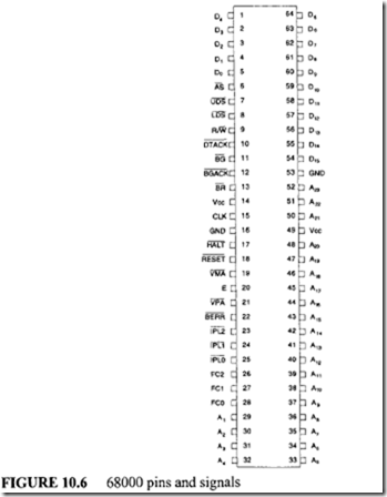
Figure 10.6 shows the 68000 pin diagram for the DIP. Appendix C provides data sheets for the 68000 and support chips.
The 68000 is provided with two Vee (+5 V) and two ground pins. Power is thus distributed in order to reduce noise problems at high frequencies. Also, to build a prototype to demonstrate that the paper design for the 68000-based microcomputer is correct, one must use either wire-wrap or solder for the actual construction. Prototype board must not be used because, at high frequencies (above 4 MHz), there will be noise problems due to stray capacitances. The 68000 consumes about 1.5 W of power.
D0-D15 are the 16 data bus pins. All transfers to and from memory and I/O devices are conducted over the 8-bit (LOW or HIGH) or 16-bit data bus depending on the size of the device. A 1-A23 are the 23 address lines. A0 is obtained by encoding the UDS {upper data strobe) and LDS (lower data strobe) lines.
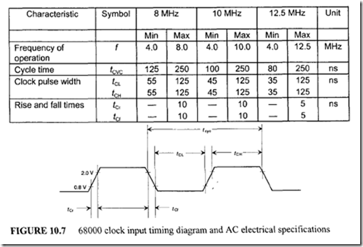
The 68000 operates on a single-phase TTL-level clock at 4, 6, 8, 10, 12.5, 16.67, or 25 MHz. The clock signal must be generated externally and applied to the 68000 clock input line. An external crystal oscillator chip is required to generate the clock. Figure I 0.7 shows the 68000 CLK waveform and clock timing specifications. The clock is at TTL compatible voltage. The clock timing specifications provide data for three different clock frequencies: 8 MHz, 10 MHz, and 12.5 MHz The 68000 CLK input can be provided by an external crystal oscillator or by designing an external circuit.
The 68000 signals can be divided into five functional categories:
1. Synchronous and asynchronous control lines
2. System control lines
3. Interrupt control lines
4. DMA control lines
5. Status lines
10.8.1 Synchronous and Asynchronous Control Lines
The 68000 bus control is asynchronous. This means that once a bus cycle is initiated, the external device must send a signal back to complete it. The 68000 also contains three synchronous control lines that facilitate interfacing to synchronous peripheral devices such as Motorola’s inexpensive MC6800 family.
Synchronous operation means that bus control is synchronized or clocked using a common system clock signal. In 6800 family peripherals, this common clock is the E clock signal depending on the particular chip used. With synchronous control, all READ and WRITE operations must be synchronized with the common clock. However, this may create problems when interfacing with slow peripheral devices. This problem D0es not arise with asynchronous bus control.
Asynchronous operation is not dependent on a common clock signal. The 68000 utilizes the asynchronous control lines to transfer data between the 68000 and peripheral devices via handshaking. Using asynchronous operation, the 68000 can be interfaced to any peripheral chip regarD1ess of the speed.
The 68000 has three control lines to transfer data over its bus in a synchronous manner: E (enable), VPA (valid peripheral address), and VMA (valid memory address). TheE clock corresponds to the clock of the 6800. TheE clock is output at a frequency that is one tenth of the 68000 input clock. VPA is an input and tells the 68000 that a 6800 device is being addressed and therefore the data transfer must be synchronized with the E clock. VMA is the processor’s response to VPA. VMA is asserted when the memory address is valid. This also tells the external device that the next data transfer over the data bus will be synchronized with the E clock.
VPA can be generated by decoding the address pins and address strobe (AS). Note that the 68000 asserts AS LOW when the address on the address bus is valid. VMA is typically used as the chip select of the 6800 peripheral. This ensures that the 6800 peripherals are selected and deselected at the correct time. The 6800 peripheral interfacing sequence is as follows:
I. The 68000 initiates a cycle by starting a normal read or write cycle.
2. The 6800 peripheral defines the 68000 cycle by asserting the 68000 VPA input.
If VPA is asserted as s00n as possible after assertion of AS, then VPA will be recognized as being asserted after three cycles. If VPA is not asserted after three cycles, the 68000 inserts wait states until VPA is recognized by the 68000 as asserted. DTACK should not be asserted while VPA is asserted. The 6800 peripheral must remove VPA within 1 clock period after AS is negated.
3. The 68000 monitors enable (E) until it is LOW. The 68000 then synchronizes all READ and WRITE operations with the E clock. The VMA output pin is asserted LOW by the 68000.
4. The 6800 peripheral waits until E is active (HIGH) and then transfers the data.
5. The 68000 waits until E goes to LOW (on a read cycle, the data is latched as E goes to LOW internally). The 68000 then negates VMA, AS, UDS, and LDS. The 68000 thus terminates the cycle and starts the next cycle.
The 68000 utilizes five lines to control address and data transfers asynchronously: AS(address strobe), R/W (read/write), DTACK (data acknowledge), UDS (upper data strobe), and LDS (lower data strobe).
The 68000 outputs to notify the peripheraJ device when data is to be transferred. AS is active LOW when the 68000 provides a valid address on the address bus. The R/W output line indicates whether the 68000 is reading data from or writing data into a peripheral device. RJW is HIGH for read and LOW for write. DTACK is used to tell the 68000 that a transfer is to be performed. When the 68000 wants to transfer data asynchronously, it first activates the AS line and at the same time generates the required address on the address lines to select the peripheral device.
Because the AS line tells the peripheral chip when to transfer data, the AS line should be part of the address decoding scheme. After enabling AS, the 68000 enters the wait state until it receives DTACK from the selected peripheral device. On receipt of DTACK, the 68000 knows that the peripheral device is ready for data transfer. The 68000 then utilizes the RJW and data lines to transfer data. UDS and LDS are defined as follows:
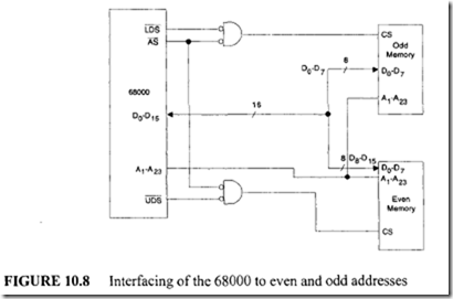
![]() A0 is encoded from UDS and LDS. When UDS is asserted, the contents of even addresses are transferred on the high-order eight lines of the data bus, Ds-D15• The 68000 internally shifts this data to the low byte of the specified register. When LDS is asserted, the contents of odd addresses are transferred on the low-order eight lines of the data bus, D0- D7. During word and long word transfers, both UDS and LDS are asserted and information is transferred on all 16 data lines, D0-D15 pins. Note that during byte memory transfers, A0 correspo ds to UDS for even addresses (A0 = 0) and to LDS for odd addresses (A0 =1). The circuit in Figure 10.8 shows how even and odd addresses are interfaced to the 68000.
A0 is encoded from UDS and LDS. When UDS is asserted, the contents of even addresses are transferred on the high-order eight lines of the data bus, Ds-D15• The 68000 internally shifts this data to the low byte of the specified register. When LDS is asserted, the contents of odd addresses are transferred on the low-order eight lines of the data bus, D0- D7. During word and long word transfers, both UDS and LDS are asserted and information is transferred on all 16 data lines, D0-D15 pins. Note that during byte memory transfers, A0 correspo ds to UDS for even addresses (A0 = 0) and to LDS for odd addresses (A0 =1). The circuit in Figure 10.8 shows how even and odd addresses are interfaced to the 68000.
10.8.2 System Control Lines
The 68000 has three control lines, BERR (bus error), HALT, and RESET, which are used to control system-related functions. BERR is an input to the 68000 and is used to inform the processor that there is a problem with the instruction cycle currently being executed. With asynchronous operation, this problem may arise if the 68000 Does not receive DTACK from a peripheral device. An external timer can be used to activate the BERR pin if the external device D0es not send DTACK within a certain period of time. On receipt ofBERR, the 68000 D0es one of the following:
-
Reruns the instruction cycle that caused the error.
-
Executes an error service routine.
The troubled instruction cycle is rerun by the 68000 if it receives a HALT signal along with the BERR signal. On receipt of LOW on both the HALT and BERR pins, the 68000 completes the current instruction cycle and then goes into the high-impedance state. On removal of both HALT and BERR (that is, when both HALT and BERR are HIGH), the 68000 reruns the troubled instruction cycle. The cycle can be rerun repeateD1y if both BERR and HALT are enabled/disabled continually.
On the other hand, an error service routine is executed only if the BERR signal is received without HALT. In this case, the 68000 will branch to a bus error vector address where the user can write a service routine. If two simultaneous bus. errors are received via the BERR pin without HALT, the 68000 automatically goes into the halt state until it is reset.
The HALT line can also be used by itself to perform single stepping or to provide DMA. When the HALT input is activated, the 68000 completes the current instruction and goes into a high-impedance state until HALT is returned to HIGH. By enabling/disabling the HALT line continually, the single-stepping debugging can be accomplished. However, because most 68000 instructions consist of more than one clock cycle, single stepping using HALT is not normally used. Rather, the trace bit in the status register is used to single-step the complete instruction.
One can also use HALT to perform microprocessor-halt DMA. Because the 68000 has separate DMA control lines, DMA using the HALT line will not normally be used. The HALT pin can also be used as an output signal. The 68000 will assert the HALT pin LOW when it goes into a halt state as a result of a catastrophic failure. The D0uble bus error (activation ofBERR twice) is an example of this type of error. When this occurs, the 68000 goes into a high-impedance state until it is reset. The HALT line informs the peripheral devices of the catastrophic failure.
The RESET line of the 68000 is also bidirectional. To reset the 68000, both the RESET and HALT pins must be LOW for 10 clock cycles at the same time except when Vee is initially applied to the 68000. In this case, an external reset must be applied for at least 100 ms. The 68000 executes a reset service routine automatically for loading the PC with the starting address of the program.
The 68000 RESET pin can also be used as an output line. A LOW can be sent to this output line by executing the RESET instruction in the supervisor mode in order to reset external devices connected to the 68000 RESET pin. Upon execution of the RESET instruction, the 68000 drives the RESET pin LOW for 124 clock periods and D0es not affect any data, address, or status registers. Therefore, the RESET instruction can be placed anywhere in the program whenever the external devices need to be reset.
Upon hardware reset, the 68000 sets the S-bit in SR to 1, and then loads the supervisor stack pointer from location $000000 (high 16 bits) and $000002 (low 16 bits) and loads the PC from $000004 (high 16 bits) and $000006 (low 16 bits); but the low 24 bits are used. In addition, the 68000 clears the trace bit in SR to 0 and sets bits 12 I I IO in SR to Ill. All other registers are unaffected.
10.8.3 Interrupt Control Lines
IPLO, IPLI, and IPL2 are the three interrupt control lines These lines provide for seven interrupt priority levels (IPL2, IPL I, IPLO = Ill means no interrupt, and IPL2, IPL I, IPLO = 000 means nonmaskable interrupt with the highest priority). The 68000 interrupts will be discussed later in this chapter.
10.8.4 DMA Control Lines
The BR (bus request), BG (bus grant), and BGACK (bus grant acknowledge) lines are used for DMA purposes. The 68000 DMA will be discussed later in this chapter.
10.8.5 Status Lines
The 68000 has the three output lines called function code pins (output lines) FC2, FCI, and FCO. These lines tell external devices whether user data/program or supervisor data/ program is being addressed. These lines can be decoded to provide user or supervisor programs/data and interrupt acknowledge as shown in Table I 0.13.
The FC2, FC I, and FCO pins can be used to partition memory into four functional areas: user data memory, user program memory, supervisor data memory, and supervisor program memory. Each memory partition can directly access up to 16 megabytes, and thus the 68000 can be made to directly address up to 64 megabytes of memory. This is shown in Figure 10.9.


