Computer Processors
and Support
I’m sure that you realize that computer processors are really just a great big sequential circuit, but I’m sure that you have no idea where to start understanding how they work. Traditional computer processors are designed using a selection of six or so basic design philosophies that give them different characteristics. In this chapter, I will introduce you to the different issues that have to be confronted in designing computer processors, along with some of the technologies that have been developed to support them.
From a high level, computer processor architects choose from making the processors ‘‘RISC’’ (‘‘Reduced Instruction Set Computers’’ – pronounced ‘‘risk’’) based or ‘‘CISC’’ (‘‘Complex Instruction Set Computers’’) based.
CISC processors tend to have a large number of instructions, each carrying out a different permutation of the same operation (accessing data directly, through index registers, etc.) with instructions perceived to be useful by the processor’s designer while RISC systems minimize the instruction set, but give them as much flexibility and access as much of the memory in the system
as possible. CISC processors also have the same requirement, but by definition, they are designed to simplify the amount of manipulation that is required by the programmer. Both computer types have their advantages and disadvantages – the RISC tends to be easier to design and executes instructions faster while the CISC tends to be easier to program but may be cumbersome in implementing some functions.
The second option processor designs have came from a competition
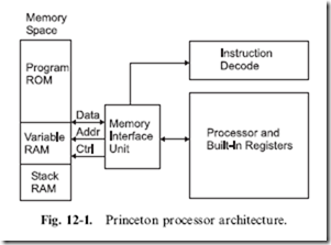
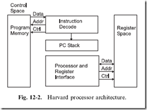
between Harvard and Princeton universities to come up with a computer architecture that could be used to compute tables of naval artillery shell distances for varying elevations and environmental conditions. Princeton’s response was for a computer that had common memory for storing the control program as well as variables and other data structures. It was best known by the chief scientist’s name ‘‘John Von Neumann’’. Figure 12-1 is a block diagram of the Princeton architecture. The ‘‘Memory Interface Unit’’ is responsible for arbitrating access to the memory space between reading instructions (based upon the current Program Counter) and passing data back and forth with the processor and its internal registers. In contrast, Harvard’s response (Fig. 12-2) was a design that used separate memory banks for program storage, the processor stack and variable RAM. By separating the data and program memories and avoiding the need to arbitrate data movements between them, there was an opportunity for programs to execute faster in Harvard’s computer.
It may at first seem that the Memory Interface Unit of the Princeton architecture is a bottleneck between the processor and the variable/RAM space – especially with the requirement for fetching instructions at the same time. In many Princeton architected processors, this is not the case because of the time required to execute an instruction is normally used
to fetch the next instruction (this is known as ‘‘pre-fetching’’). Other processors (most notably the processor in your PC) have separate program and data ‘‘caches’’ that can be accessed directly while other address accesses are taking place.
The Princeton architecture won the competition because it was better suited to the technology of the time. Using one memory was preferable because of the unreliability of then current electronics (this was before transistors were in widespread general use): a single memory and associated interface would have fewer things that could fail. The Harvard architecture is really best for processor applications that do not process large amounts of memory from different sources (which is what the Von Neumann architecture is best at) and be able to access this small amount of memory very quickly.
Once the processor’s instruction set philosophy and architecture have been decided upon, the design of the processor is then passed to the engineers responsible for implementing the design in silicon. Most of these details are left ‘‘under the covers’’ and do not affect how the application designer interfaces with the application. There is one detail that can have a big effect on how applications execute, and that is whether or not the processor is a ‘‘hardcoded’’ or ‘‘microcoded’’ device. Each processor instruction is in fact a series of instructions that are executed to carry out the instruction. For example, to load the accumulator in a processor, the following steps could be taken:
1. Output Address in Instruction to the Data Memory Address Bus Drivers.
2. Configure Internal Bus for Data Memory value to be stored in Accumulator.
3. Enable Bus Read.
4. Compare Data read in to zero or any other important conditions and set bits in the ‘‘STATUS’’ Register.
5. Disable Bus Read.
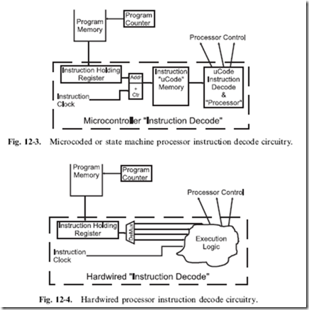
A microcoded processor is really a computer processor within a processor. In a microcoded processor, a ‘‘state machine’’ executes each different instruction as the address to a subroutine of instructions. When an instruction is loaded into the ‘‘Instruction Holding Register’’, certain bits of the instruction are used to point to the start of the instruction routine (or microcode) and the ‘‘uCode Instruction Decode and Processor’’ Logic executes the microcode instructions until an ‘‘instruction end’’ is encountered. This is shown in Fig. 12-3.
A ‘‘hardwired’’ processor uses the bit pattern of the instruction to access specific logic gates (possibly unique to the instruction) which are executed as a combinatorial circuit to carry out the instruction. Figure 12-4 shows how
the instruction loaded into the Instruction Holding Register is used to initiate a specific portion of the ‘‘Execution Logic’’ which carries out all the functions of the instruction.
Each of the two methods offers advantages over the other. A microcoded processor is usually simpler than a hardwired one to design and can be
implemented faster with less chance of having problems at specific conditions. If problems are found, revised ‘‘steppings’’ of the silicon can be made with a relatively small amount of design effort. The hardwired processor tends to execute instructions much faster but is much harder to modify.
IEEE754 Floating Point Numbers
When I introduced binary numbers earlier in the book, I discussed binary integers, but I did not discuss how binary ‘‘real’’ numbers were produced or how they were manipulated in workstation processors. It should not be a surprise to discover that binary floating point numbers are analogous to decimal floating point numbers.
For example, if you were going to convert decimal 7.80 to binary, you would first convert the value equal to or greater than one to binary.
Decimal 7 becomes B’0111’, leaving decimal 0.80 to convert. This is accomplished by knowing that decimal fraction digits are multiplied by negative exponents of the base 10. The same methodology can be used for binary numbers.
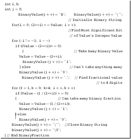
To convert decimal 0.80 to a binary fraction, I will start with the exponent ‘‘-1’’ which is equal to 0.5 decimal and test to see if it can be removed from the fraction. Since it can, my binary number becomes B’0111.1’ with a remainder of 0.30. Going to the next negative exponent (‘‘-2’’), I discover that I can subtract this value, giving me the binary value B’0111.11’. Continuing this on for another four bits, the binary value is B’0111.110011’. It’s interesting to see that the binary number is irrational; the bit pattern will change the smaller the fraction that is calculated even though the decimal number ends at the first digit after the decimal point.
This method can be expressed as the ‘‘C’’ function, which converts the floating point number to a binary string:
This operation can be performed within high-performance processors (like the Intel Pentium), but instead of producing a string of characters represent- ing binary data, they generally put them into the IEEE754 format, which stores the floating binary value in a format which is similar to that of ‘‘Scientific Notation’’:
The ‘‘Mantissa’’ is multiplied by the signed exponent to get values less than or greater than one.
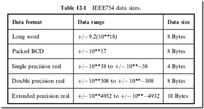
Table 12-1 lists the data formats supported by the Intel Pentium. These different formats give you a lot of flexibility to work with a wide range of numbers in different applications. All the number formats can be processed together, with the final result being in the most accurate format (i.e. a ‘‘word’’ and ‘‘single precision’’ combined together will have a result as a single precision number).
Memory Types
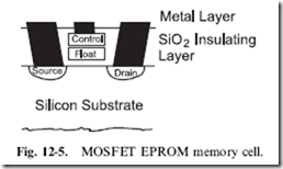
A number of different memory types are currently available. In this introduction, I will first show you three different technologies and discuss where (and why) they are used in a computer system. The boot up, non-volatile memory used in a computer system is based on ultraviolet light ‘‘Erasable PROM’’ (‘‘EPROM’’) program memory (Fig. 12-5) and was first introduced in the late 1960s. An EPROM memory cell consists of a transistor
that can be set to be always ‘‘on’’ or ‘‘off’’. Figure 12-5 shows the side view of the EPROM transistor.
The EPROM transistor is a MOSFET-like transistor with a ‘‘floating’’ gate surrounded by silicon dioxide above the substrate of the device. ‘‘Silicon dioxide’’ is best known as ‘‘glass’’ and is a very good insulator. To program the floating gate, the ‘‘Control’’ gate above the floating gate is raised to a high enough voltage potential to have the silicon dioxide surrounding it to ‘‘break down’’ and allow a charge to pass into the floating gate. With a charge in the floating gate, the transistor is turned ‘‘on’’ at all times, until the charge escapes (which will take a very long time that is usually measured in tens of years).
An improvement over UV erasable EPROM technology is ‘‘Electrically Erasable PROM’’ (‘‘EEPROM’’). This non-volatile memory is built with the same technology as EPROM, but the floating gate’s charge can be removed by circuits on the chip and no UV light is required. There are two types of EEPROM available. The first type is simply known as ‘‘EEPROM’’ and allows each bit (and byte) in the program memory array to be reprogrammed without affecting any other cells in the array. This type of memory first became available in the early 1980s.
In the late 1980s, Intel introduced a modification to EEPROM that was called ‘‘Flash’’. The difference between Flash and EEPROM is Flash’s use of a bussed circuit for erasing the cells’ floating gates rather than making each cell independent. This reduced the cost of the EEPROM memory and speeded up the time required to program a device (rather than having to erase each cell in the EEPROM individually, in Flash the erase cycle, which takes as long for one byte, erases all the memory in the array).
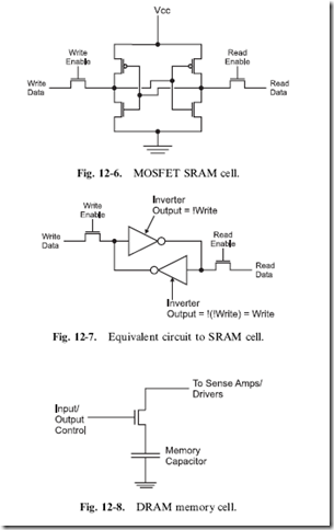
For high-speed storage, data is saved in ‘‘Static Random Access Memory’’ (‘‘SRAM’’) which will retain the current contents as long as power is applied to it and is known as ‘‘volatile’’ memory. This is in contrast to the ‘‘EPROM’’ or Flash, which does not loose its contents when power is taken away but cannot have its contents changed as easily as ‘‘SRAM’’. Each bit in a SRAM memory array is made up of the six transistor memory cell, as shown in Fig. 12-6. This memory cell will stay in one state until the ‘‘Write Enable’’ transistor is enabled and the write data is used to set the state of the SRAM cell.
The SRAM cell could be modeled as the two inverters shown in Fig. 12-7. Once a value has been set in the inverters’ feedback loop it will stay there until changed. Reading data is accomplished by asserting the read enable line and inverting the value output (because the ‘‘read’’ side contains the inverted ‘‘write’’ side’s data). The driver to the SRAM cell must be able to ‘‘overpower’’ the output of the inverter in order for it to change state.
The outputs of the inverters are usually current limited to avoid any backdriving concerns.
Large, inexpensive and reasonably high-speed memory can be built from ‘‘Dynamic Random Access Memory’’ (‘‘DRAM’’) cells. You may have heard the term ‘‘Single Transistor Memory Cells’’ for descriptions of DRAM and that’s actually a pretty good description of each cell, which is shown in Fig. 12-8.
In DRAM memory cell, the transistor is used as a switch to allow a charge to be moved into or out of the capacitor. For a write, the transistor is turned on and a charge is either pushed into or pulled out of the capacitor. When the transistor is turned off, the charge is trapped in the capacitor and cannot change until the transistor is turned on again.
A DRAM read is accomplished by turning on the transistor and any charge that is in the capacitor will leak out and will be detected and amplified by a ‘‘Sense Amplifier’’. The ‘‘Sense Amp’’ is a metastable flip flop that will be set to the state of the capacitor when the transistor switch is closed. Before the transistor is turned on when writing to the cell, the sense amp will be set to a specific state to load the correct charge into the capacitor.
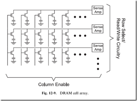
In a DRAM memory chip, the cells are arranged in rows and columns, as shown in Fig. 12-9. To address each cell within the chip, a row/column address for the element in the array has to be provided. Usually, to save pins on the DRAM chips, the row and column address lines are shared (multiplexed) together so that during a read or a write, first the ‘‘Row’’ is selected and then the ‘‘Column’’.
The row is selected first so that if a write is taking place the sense amp for the row can be set to the specific value. All the other sense amps are set in their metastable state. When the Column address is latched in, the transistors for the array row are turned on. Next, when the row address is available, the
place. For the cells not being written to, the sense amps will not only read what the charge is in the capacitor but will also ‘‘refresh’’ it as well.
This is a very good thing in DRAM because the capacitor is actually a MOS transistor built into the chip, acting as a capacitor. Over time, any charge in this capacitor will leak away into the silicon substrate. By periodically ‘‘refreshing’’ the charge by performing a read (which will cause the sense amps to amplify the charge), the contents of the memory will never be lost.
Refreshing is typically done by enabling all the transistors in a column (without first specifying a row) and letting the sense amps do their thing. A read of an incrementing column address is usually implemented in the DRAM support hardware and is known as a ‘‘CAS (‘‘Column Address Strobe’’) Only Refresh’’. In the original PC, 5% of the processor bandwidth was lost due to DRAM refresh requirements. To overcome these potential deficiencies, PC designers have come up with a few hardware features.
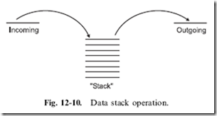
Along with being arranged as simple, single-dimensional arrays of data, memory can also be built into ‘‘stacks’’ (Fig. 12-10). Processor stacks are a simple and fast way of saving data during program execution. Stacks save data in a processor the same way you save papers on your desk and is known as ‘‘last in/first out’’ (‘‘LIFO’’) memory. As you are working, the work piles up in front of you and you do the task that is at the top of the pile.
