The 8086 Microprocessor
1. Draw the pin diagram of 8086.
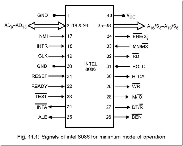
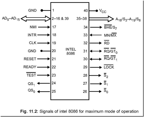
Ans. There would be two pin diagrams—one for MIN mode and the other for MAX mode of 8086, shown in Figs. 11.1 and 11.2 respectively. The pins that differ with each other in the two modes are from pin-24 to pin-31 (total 8 pins).
2. What is the technology used in 8086 µP?
Ans. It is manufactured using high performance metal-oxide semiconductor (HMOS) technology. It has approximately 29,000 transistors and housed in a 40-pin DIP package.
3. Mention and explain the modes in which 8086 can operate. Ans. 8086 µP can operate in two modes—MIN mode and MAX mode.
When MN/MX pin is high, it operates in MIN mode and when low, 8086 operates in MAX mode.
For a small system in which only one 8086 microprocessor is employed as a CPU, the system operates in MIN mode (Uniprocessor). While if more than one 8086 operate in a system then it is said to operate in MAX mode (Multiprocessor).
The bus controller IC (8288) generates the control signals in case of MAX mode, while in MIN mode CPU issues the control signals required by memory and I/O devices.
4. Distinguish between the lower sixteen address lines from the upper four.
Ans. Both the lower sixteen address lines (AD0 − AD15 ) and the upper four address lines
(A16 / S3 − A19 / S6 ) are multiplexed.
During T1, the lower sixteen lines carry address (A0 − A15 ) , while during T2, T3 and T4 they carry data.
Similarly during T1, the upper four lines carry address (A16– A19), while during T2,
T3 and T4 , they carry status signals.
5. In how many modes the minimum-mode signal can be divided?
Ans. In the MIN mode, the signals can be divided into the following basic groups: address/data bus, status, control, interrupt and DMA.
6. Tabulate the common signals, Minimum mode signals and Maximum mode signals. Also mention their functions and types.
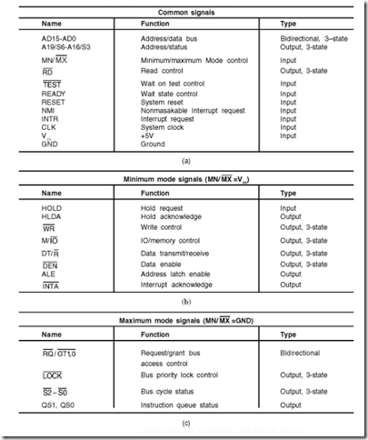
Ans. Table 11.1 shows the common signals, Minimum mode signals and the Maximum mode signals, along with the functions of each and their types.
Table 11.1 : (a) Signals common to both minimum and maximum mode, (b) Unique minimum-mode signals, (c) Unique maximum-mode signals for 8086.
7. Mention the different varieties of 8086 and their corresponding speeds.
Ans. The following shows the different varieties of 8086 available and their corresponding speeds.
Types Speeds
8086 5 MHz
8086–1 10 MHz
8086–2 8 MHz
8. Mention (a) the address capability of 8086 and (b) how many I/O lines can be accessed by 8086.
Ans. 8086 addresses via its A0–A19 address lines. Hence it can address 220 = 1MB memory.
Address lines A0 to A15 are used for accessing I/O’s. Thus, 8086 can access 216 = 64
KB of I/O’s.
9. What is meant by microarchitecture of 8086?
Ans. The individual building blocks of 8086 that, as a whole, implement the software and hardware architecture of 8086. Because of incorporation of additional features being necessitated by higher performance, the microarchitecture of 8086 or for that matter any microprocessor family, evolves over time.
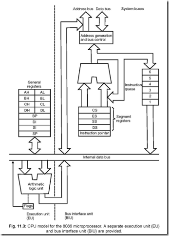
10. Draw and discuss the architecture of 8086. Mention the jobs performed by BIU and EU.
Ans. The architecture of 8086 is shown below in Fig. 11.3. It has got two separate functional units—Bus Interface Unit (BIU) and Execution Unit (EU).
8086 architecture employs parallel processing—i.e., both the units (BIU and EU) work at the same time. This is Unlike 8085 in which Sequential fetch and execute operations take place. Thus in case of 8086, efficient use of system bus takes place and higher performance (because of reduced instruction time) is ensured.
z BIU has segment registers, instruction pointer, address generation and bus control logic block, instruction queue while the EU has general purpose registers, ALU, control unit, instruction register, flag (or status) register.
The main jobs performed by BIU are:
z BIU is the 8086’s interface to the outside world, i.e., all External bus operations
are done by BIU.
z It does the job of instruction fetching, reading/writing of data/operands for memory
and also the inputting/outputting of data for peripheral devices.
z It does the job of filling the instruction queue.
z Does the job of address generation.
The main jobs performed by the execution unit are:
z Decoding/execution of instructions.
z It accepts instructions from the output end of instruction queue (residing in BIU)
and data from the general purpose registers or memory.
z It generates operand addresses when necessary, hands them over to BIU
requesting it (BIU) to perform read or write cycle to memory or I/O devices.
z EU tests the status of flags in the control register and updates them when
executing instructions.
z EU waits for instructions from the instruction queue, when it is empty.
z EU has no connection to the system buses.
11. Explain the operations of instructions queue residing in BIU.
Ans. The instruction queue is 6-bytes in length, operates on FIFO basis, and receives the instruction codes from memory. BIU fetches the instructions meant for the queue ahead of time from memory. In case of JUMP and CALL instructions, the queue is dumped and newly formed from the new address.
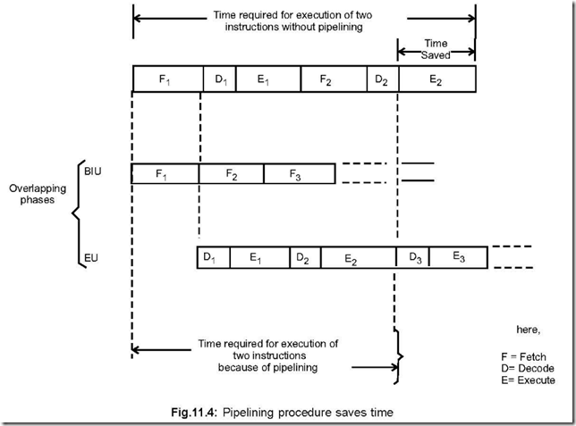
Because of the instruction queue, there is an overlap between the instruction execution and instruction fetching. This feature of fetching the next instruction when the current instruction is being executed, is called Pipelining.
Fig. 11.4, which is self-explanatory, shows that there is definitely a time saved in case of overlapping phases (as in the case of 8086) compared to sequential phases (as in the case of 8085). Initially, the queue is empty and CS : IP is loaded with the required address (from which the execution is to be started). Microprocessor 8086 starts operation by fetching
1 (or 2) byte(s) of instruction code(s) if CS : IP address is odd (even).
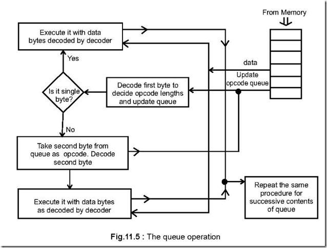
The 1st byte is always an opcode, which when decoded, one byte in the queue becomes empty and the queue is updated. The filling in operation of the queue is not started until two bytes of the instruction queue is empty. The instruction execution cycle is never broken for fetch operation.
After decoding of the 1st byte, the decoder circuit gets to know whether the instruction is of single or double opcode byte.
For a single opcode byte, the next bytes are treated as data bytes depending upon the decoded instruction length, otherwise the next byte is treated as the second byte of the instruction opcode.
For a 2-byte instruction code, the decoding process takes place taking both the bytes into consideration which then decides on the decoded instruction length and the number of subsequent bytes which will be treated as instruction data. Updation of the queue takes place once a byte is read from the queue.
The queue operation is shown in Fig. 11.5 in block schematic form.
12. Mention the conditions for which EU enters into WAIT mode.
Ans. There are three conditions that cause the EU to enter into WAIT state. These are:
z When an instruction requires the access to a memory location not in the queue.
z When a JUMP instruction is executed. In this case the current queue contents are
aborted and the EU waits until the instructions at the jump address is fetched from
memory.
z During execution of instruction which are very slow to execute. The instruction AAM
(ASCII adjust for multiplication) requires 83 clock cycles for execution. For such a
case, the BIU is made to wait till EU pulls one or two bytes from the queue before
resuming the fetch cycle.
13. Mention the kind of operations possible with 8086.
Ans. It can perform bit, byte, word and block operations. Also multiplication and division operations can be performed by 8086.
14. Mention the total number of registers of 8086 and show the manner in which they are grouped.
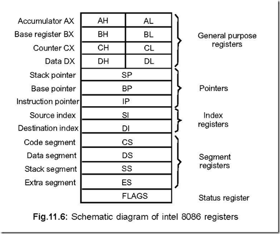
Ans. There are in all fourteen numbers of 16-bit registers. The different groups are made as hereunder:
z Data group, pointers and index group, status and control flag group and segment group.
z The data group consists of AX (accumulator), BX (base), CX (count) and DX (data).
z Pointer and Index group consist of SP (Stack pointer), BP (Base pointer), SI (Source
Index), DI (Destination index) and IP (Instruction pointer).
z Segment group consists of ES (Extra Segment), CS (Code Segment), DS (Data
Segment) and SS (Stack Segment).
z Control flag group consists of a single 16-bit flag register.
Fig. 11.6 shows the registers placed in the different groups to form a programming
model.
15. Describe, in detail, the general purpose of data registers.
Ans. Fig. 11.7 shows the four data registers along with their dedicated functions also.
All the four registers can be used bytewise or wordwise. The alphabets X, H and L respectively refer to word, higher byte or lower byte respectively of any register.
All the four registers can be used as the source or destination of an operand during an arithmetic operation such as ADD or logical operation such as AND, although particular registers are earmarked for specific operations. Register C is used as a count register in string operations and as such is called a ‘count’ register. Register C is also used for multibit shift or rotate instructions.
Register D is used to hold the address of I/O port while register A is used for all I/O operations that require data to be inputted or outputted.
16. Describe the status register of 8086.
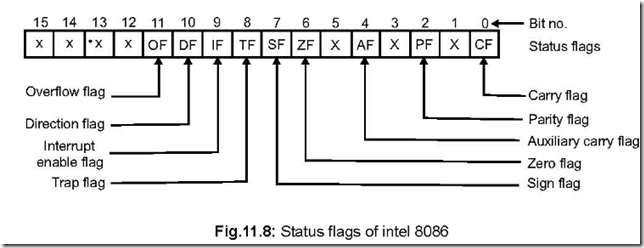
![]() Ans. It is a 16-bit register, also called flag register or Program Status Word (PSW). Seven bits remain unused while the rest nine are used to indicate the conditions of flags. The status flags of the register are shown below in Fig. 11.8.
Ans. It is a 16-bit register, also called flag register or Program Status Word (PSW). Seven bits remain unused while the rest nine are used to indicate the conditions of flags. The status flags of the register are shown below in Fig. 11.8.
Out of nine flags, six are condition flags and three are control flags. The control flags are TF (Trap), IF (Interrupt) and DF (Direction) flags, which can be set/reset by the programmer, while the condition flags [OF (Overflow), SF (Sign), ZF (Zero), AF (Auxiliary Carry), PF (Parity) and CF (Carry)] are set/reset depending on the results of some arithmetic or logical operations during program execution.
CF is set if there is a carry out of the MSB position resulting from an addition
operation or if a borrow is needed out of the MSB position during subtraction.
PF is set if the lower 8-bits of the result of an operation contains an even number of 1’s. AF is set if there is a carry out of bit 3 resulting from an addition operation or a borrow required from bit 4 into bit 3 during subtraction operation.
ZF is set if the result of an arithmetic or logical operation is zero.
SF is set if the MSB of the result of an operation is 1. SF is used with unsigned
numbers.
OF is used only for signed arithmetic operation and is set if the result is too large to be fitted in the number of bits available to accommodate it.
The functions of the flags along with their bit positions are shown in Fig. 11.9 below.
17. Discuss the three control flags of 8086.
Ans. The three control flags of 8086 are TF, IF and DF. These three flags are programmable, i.e., can be set/reset by the programmer so as to control the operation of the processor.
When TF (trap flag) is set (=1), the processor operates in single stepping mode—i.e.,
pausing after each instruction is executed. This mode is very useful during program development or program debugging.
When an interrupt is recognised, TF flag is cleared. When the CPU returns to the
main program from ISS (interrupt service subroutine), by execution of IRET in the last line of ISS, TF flag is restored to its value that it had before interruption.
TF cannot be directly set or reset. So indirectly it is done by pushing the flag register
on the stack, changing TF as desired and then popping the flag register from the stack.
When IF (interrupt flag) is set, the maskable interrupt INTR is enabled otherwise
disabled (i.e., when IF = 0).
IF can be set by executing STI instruction and cleared by CLI instruction. Like TF flag, when an interrupt is recognised, IF flag is cleared, so that INTR is disabled. In the last line of ISS when IRET is encountered, IF is restored to its original value.
When 8086 is reset, IF is cleared, i.e., resetted.
DF (direction flag) is used in string (also known as block move) operations. It can be
set by STD instruction and cleared by CLD. If DF is set to 1 and MOVS instruction is
executed, the contents of the index registers DI and SI are automatically decremented to access the string from the highest memory location down to the lowest memory location.
18. Discuss the Pointers and Index group of registers.
Ans. The pointer registers are SP and BP while the index registers are SI and DI.
All the four are 16-bit registers and are used to store offset addresses of memory
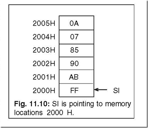
locations relative to segment registers. They act as memory pointers. As an example, MOV AH, [SI] implies, “Move the byte whose address is contained in SI into AH”. If now, SI = 2000 H, then execution of above instruction will put the value FF H in register AH, shown in Fig. 11.10, [SI+1 : SI] = ABFF H, where obviously SI+1 points to memory location 2001 H and [SI+1] = AB H.
SI and DI are also used as general purpose registers. Again in certain string (block
move) instructions, SI and DI are used as source and destination index registers
respectively. For such cases, contents of SI are added to contents of DS register to get the actual source address of data, while the contents of DI are added to the contents of ES to get the actual destination address of data.
SP and BP stand for stack pointer and base pointer with SP containing the offset address or the stack top address. The actual stack address is computed by adding the contents of SP and SS.
Data area(s) may exist in stack. To access such data area in stack segment, BP register is used which contains the offset address. BP register is also used as a general purpose register.
Instruction pointer (IP) is also included in the index and pointers group. IP points to the offset instead of the actual address of the next instruction to be fetched (from the current code segment) in BIU. IP resides in BIU but cannot be programmed by the programmer.
19. Describe in brief the four segment registers.
Ans. The four segment registers are CS, DS, ES and SS—standing for code segment register, data segment register, extra segment register and stack segment register respectively. When a particular memory is being read or written into, the corresponding memory address is determined by the content of one of these four segment registers in conjunction with their offset addresses.
The contents of these registers can be changed so that the program may jump from one active code segment to another one.
The use of these segment registers will be more apparent in memory segmentation schemes.
20. Discuss A16/S3—A19/S6 Signals of 8086.
Ans. These are time multiplexed signals. During T1, they represent A19 – A16 address lines.
During I/O operations, these lines remain low. During T2–T4, they carry status signals.
S4 and S3 (during T2 to T4) identify the segment register employed for 20-bit physical
address generation.
Status signal S5 (during T2 to T4) represents interrupt enable status. This is updated at the beginning of each clock cycle.
Status signal S6 remains low during T2to T4 .
21. Discuss BHE/S7 signal.
Ans. During T1, this becomes bus high enable signal and remains low while during T2 to T4 it acts as a status signal S7 and remains high during this time.
During T1, when BHE signal is active, i.e., remains low, it is used as a chip select signal on the higher byte of data bus—i.e., D15–D8.
Table 11.2 shows BHE and A0 signals determine one of the three possible references to memory.
22. Discuss the Reset pin of 8086.
Ans. Reset is an active high input signal and must be active for at least 4 CLK cycles to be accepted by 8086. This signal is internally synchronised and execution starts only after Reset returns to low value.
For proper initialisation, Reset pulse must not be applied before 50µS of ‘power on’
of the circuit. During Reset state, all three buses are tristated and ALE and HLDA are driven low.
During resetting, all internal register contents are set to 0000 H, but CS is set to F000 H and IP to FFF0 H. Thus execution starts from physical address FFFF0 H. Thus EPROM in 8086 is interfaced so as to have the physical memory location forms FFFF0 H to FFFFF H, i.e., at the end of the map.
23. Discuss the two pins (a) DT/ R and (b) DEN .
Ans. (a) DT/ R is an output pin which decides the directions of data flow through the transreceivers (bidirectional buffers).
When the processor sends out data, this signal is 1 while when it receives data,
the signal status is 0.
(b) DEN stands for data enable. It is an active low signal and indicates the availability of data over the address/data lines. This signal enables the transreceivers to separate data from the multiplexed address/data signal. It is active from the middle of T2 until
the middle of T4.
Both DT/ R and DEN are tristated during ‘hold acknowledge’.
24. Elaborate the functions of the pins S2 , S1 and S0 .
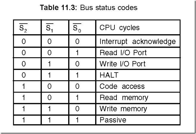
Ans. These three are output status signals in the MAX mode, indicating the type of operation carried out by the processor.
The signals become active during T4 of the previous cycle and remain active during T1 and T2 of the current cycle. They return to the passive state during T3 of the current bus cycle so that they may again become active for the next bus cycle during T4. Table
11.3 shows the different bus cycles of 8086 for different combinations of these three
signals.
25.Explain the LOCK signal.
Ans. It is an active low output signal and is activated by LOCK prefix instruction and remains active until the completion of the next instruction. It floats to tri-state during hold
![]() acknowledge when LOCK signal is low, all interrupts get masked and HOLD request is not granted. LOCK signal is used by the processor to prevent other devices from
acknowledge when LOCK signal is low, all interrupts get masked and HOLD request is not granted. LOCK signal is used by the processor to prevent other devices from
accessing the system control bus. This symbol is used when CPU is executing some critical instructions and through this signal other devices are informed that they should not issue HOLD signal to 8086.
![]() Ans. It is an active low input signal. Normally the BUSY pin (output) of 8087 NDP is connected to the TEST input pin of 8086. When maths co-processor 8087 is busy executing some
Ans. It is an active low input signal. Normally the BUSY pin (output) of 8087 NDP is connected to the TEST input pin of 8086. When maths co-processor 8087 is busy executing some
![]() instructions, it pulls its BUSY signal high. Thus the TEST signal of 8086 is consequently high, and it (8086) is made to WAIT until the BUSY signal goes low. When 8087
instructions, it pulls its BUSY signal high. Thus the TEST signal of 8086 is consequently high, and it (8086) is made to WAIT until the BUSY signal goes low. When 8087
![]() completes its instruction executions, BUSY signal becomes low. Thus the TEST input of 8086 becomes low also and then only 8086 goes in for execution of its program.
completes its instruction executions, BUSY signal becomes low. Thus the TEST input of 8086 becomes low also and then only 8086 goes in for execution of its program.
27. Show how demultiplexing of address/data bus is done and also show the availability of address/data during read/write cycles.
Ans. The demultiplexing of lower 2-bytes of address/data bus (AD0–AD15) is done by 8282/8283 octal latch with 8282 providing non-inverting outputs while 8283 gives out inverted outputs. The chip outputs are also buffered so that more drive is available at their outputs.
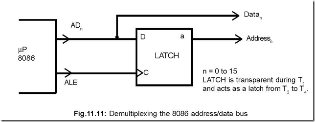
A D latch is central to the demultiplexing operations of these latches. During T1 when ALE is high, the latch is transparent and the output of latch is ‘A’ (address) only. At the end of T1, ALE has a high to low transition which latches the address available at the D input of the latch, so that address is continued to be available from the Q output of the latch (i.e., whole of T1 to T4 states).
It is to be noted that memory and I/O devices do not access the data bus until the
beginning of T2, thus the ‘data’ is a ‘don’t care’ till the end of T1. This is shown in Fig. 11.11 and the timing diagram shows the availability of data for read and write cycles.
28. Discuss the Instruction Pointer (IP) of 8086.
Ans. Functionally, IP plays the part of Program Counter (PC) in 8085. But the difference is that IP holds the offset of the next word of the instruction code instead of the actual address (as in PC).
IP along with CS (code segment) register content provide the 20-bit physical (or real) address needed to access the memory. Thus CS:IP denotes the value of the memory address of the next code (to be fetched from memory).
Content of IP gets incremented by 2 because each time a word of code is fetched from memory.
29. Indicate the data types that can be handled by 8086 µP.
Ans. The types of data formats that can be handled by 8086 fall under the following categories:
z Unsigned or signed integer numbers—both byte-wide and word-wide.
z BCD numbers—both in packed or unpacked form.
z ASCII coded data. ASCII numbers are stored one number per byte.
30. Compare 8086 and 8088 microprocessors.
Ans. The Comparison between the two is tabulated below in Table 11.4.
|
31. Comment on the instruction size of 8086. Ans. It varies from 1 to 6 bytes.
32. Discuss the instruction format of 8086.
Ans. The instruction format of 8086 is shown in Fig. 11.12. It is extendable up to 6-bytes. The first byte contains D and W—Direction Register Bit and Data Size Bit respectively. Both D and W are 1-bit in nature.
z If D = 1, then register operand existing in byte-2 is the destination operand, otherwise (i.e., if D = 0) it is a source operand.
z W indicates whether the operation is an 8-bit or a 16-bit data. If W = 0 then it is an
8-bit operation, else (i.e., W = 1) it is 16-bit one.
z The 2nd byte (byte-2) indicates whether one of the operands is in memory or both are in registers. This byte contains three fields:
|
Field |
Abbreviation |
Length (no. of bits) |
|
Mode field |
MOD |
2 |
|
Register field |
REG |
3 |
|
Register/Memory field |
r/m |
3 |
33. Discuss the MOD and r/m and REG fields.
Ans. MOD field is a 2-bit field. It addresses memory in the following manner.
MOD field values
0 0 ====>Memory addressing without displacement
0 1 ====>Memory addressing with 8-bit displacement
1 0====> Memory addressing with 16-bit displacement
1 1 ====>Register addressing with
W = 0 for 8-bit data
and W = 1 for 16-bit data
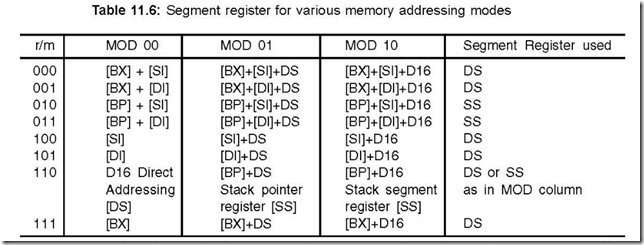
The r/m field which is a 3-bit field, along with MOD field defines the 2nd operand. If MOD = 11, then it is a register to register mode. Again if MOD = 00,01 or 10 then it is a memory mode. Table 11.5 shows how effective address of memory operand gets selected for MOD = 00,01 and 10 values.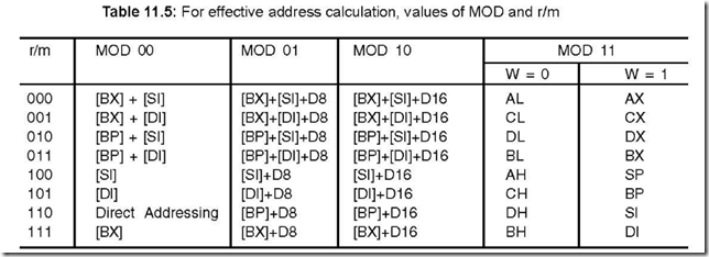
Again, for MOD values 00,01 and 10, the default segment registers selected are shown in Table 11.6.
The REG field is a 3-bit field and indicates the register for the first operand which can be source/destination operand, depending on D = 0/1.
How REG field along with the status of W(0 or 1) select the different registers, is shown in Table 11.7.
34. Discuss the instruction format for segment override prefix.
Ans. Default segment selection can be overriden by the override prefix byte, as shown in below.
Depending on the 2-bit rr values, the segments selected are shown in Table 11.8.
The override prefix byte follows the opcode byte of the instruction, whenever used.
35. Is direct memory to memory data transfer possible in 8086?
Ans. No, 8086 does not have provision for direct memory to memory data transfer. For this to be implemented, AX is used as an intermediate stage of data. The source byte (from the memory) is moved into AX register with one instruction. The second instruction moves the content of AX into destination location (into another memory location). As example,
MOV AH, [SI]
MOV [DI], AH
Here, the first instruction moves the content of memory location, whose offset
address remains in SI, into AH. The second instruction ensures that the content of AH
is moved into another memory location whose offset address is in DI.
36. Can the data segment (DS) register be loaded directly by its address?
Ans. No, it cannot be done directly. Instead, AX is loaded with the initial address of the DS register and then it is transferred to DS register, as shown below:
MOV AX, DS ADDR: AX is loaded with initial address of DS register
MOV DS, AX: DS is loaded with AX, i.e., ultimately with DS ADDR
37. Show, in tabular form, the default and alternate segment registers for different types of memory references.
Ans. Table 11.9 shows the default and alternate register segments which can be used for different types of memory references.

![The 8086 Microprocessor 8-56-12 PM_thumb[1] The 8086 Microprocessor 8-56-12 PM_thumb[1]](http://lh4.ggpht.com/-DXoU3bgyB5A/VEu70HWokhI/AAAAAAAAqhQ/9T0jJW_qdYU/The%2525208086%252520Microprocessor%2525208-56-12%252520PM_thumb%25255B1%25255D_thumb.png?imgmax=800)
![The 8086 Microprocessor 8-57-20 PM_thumb[1] The 8086 Microprocessor 8-57-20 PM_thumb[1]](http://lh5.ggpht.com/-KzuBgLLZeDQ/VEu8AiezLFI/AAAAAAAAqhw/pqEmflfVlqU/The%2525208086%252520Microprocessor%2525208-57-20%252520PM_thumb%25255B1%25255D_thumb.png?imgmax=800)

![The 8086 Microprocessor 9-00-29 PM_thumb[1] The 8086 Microprocessor 9-00-29 PM_thumb[1]](http://lh5.ggpht.com/-WBHRHFs7_5o/VEu821iu0pI/AAAAAAAAqkg/tpJpVDVrDZs/The%2525208086%252520Microprocessor%2525209-00-29%252520PM_thumb%25255B1%25255D_thumb.png?imgmax=800)

![The 8086 Microprocessor 9-01-10 PM_thumb[1] The 8086 Microprocessor 9-01-10 PM_thumb[1]](http://lh5.ggpht.com/-cNZLAk9z6IQ/VEu89jlbt0I/AAAAAAAAqlA/A90xq_Z1WGQ/The%2525208086%252520Microprocessor%2525209-01-10%252520PM_thumb%25255B1%25255D_thumb.png?imgmax=800)