Memory
1. What is a memory?
Ans. A memory is a device that stores information in electrical, magnetic or optical form. A
µC based system, which operates on digital logic, holds binary information. Semiconductor
memories are used in µC based system.
2. Why semiconductor memories are used as main memories in mC based systems?
Ans. Semiconductor memories have become very popular and widely used because of their high reliability, low cost, high speed and ease with which memory size can be expanded.
3. What is the use of memory in a mC based system? Ans. Memories are used for storage of both program and data.
4. In how many categories memories can be classified? Give examples and distinguish between them.
Ans. It can be categorised into two ways:
z Primary memory or main memory or working memory.
z Secondary memory or auxiliary memory or mass storage.
RAM and ROM comprise the primary memory while magnetic tapes, magnetic disks,
floppy disks or compact disks (CDs) are examples of secondary memory.
Distinction between the two types of memories are:
Table 8.1: Comparison between primary and secondary memory
|
S. No. |
Primary memory |
Secondary memory |
|
|
1. |
Can store less amount of data. |
1. |
Can store huge amount of data. |
|
2. |
Faster speed of operation. |
2. |
Slower speed of operation. |
|
3. |
Can be volatile/non-volatile in nature. |
3. |
Always non-volatile in nature. |
|
4. |
Program/data used by the programmer |
4. |
Not used for such purpose. |
|
are resident in the main memory. |
|||
|
5. |
Can be directly accessed by CPU. |
5. |
Cannot be directly accessed by CPU but |
|
can be accessed through I/O ports or in |
|||
|
a serial format using hardware/software. |
|||
|
6. |
If the CPU has n address lines, a |
6. |
No such relation exists. |
|
maximum of 2n main memory locations |
|||
|
can be accessed. |
|||
|
7. |
Less costly. |
7. |
Costlier than main memory. |
5. What is the basic memory operation?
Ans. ‘Read’ and ‘Write’ are the basic operations performed by a memory device. The process of storing data into memory is called ‘Writing’ and retrieving data/instruction from the memory is called ‘Reading’. Each memory location is identified by a particular address corresponding to the memory location. For reading or writing data, the particular memory location is to be identified by its address first and then only reading/writing is done.
6. What is a cell?
Ans. Memories are made of storage elements, which can store one bit of data. Each storage element is called a cell. In semiconductor memories, flip-flops act as storage elements.
7. What is meant by ‘working length’ of a memory?
Ans. At each memory location, which is identified by its address, one or more number of bits can be stored. The number of bits that a particular memory location can store is known as working length of a memory. This also goes by the name of word size.
8. What is meant by “access time” of a memory? On which does it depend?
Ans. It is the time required to perform a read operation. Putting another way, it is the time between the memory receiving a new address and putting out the memory content on its output. This time is symbolised by tacc.
9. What is a sequential access memory (SAM)?
Ans. It is a kind of memory for which tacc is not constant for all memory locations/positions.
An example of a SAM is a magnetic tape backup. The latter the data is stored, the more
the tacc time for such a data. SAM is used only when data retrieval is always sequential in nature.
10. What is a volatile memory?
Ans. It is such a memory whose stored information is lost when electrical power is removed.
Semiconductor memories may be volatile/non-volatile in nature, while magnetic memories are non-volatile.
11. A semiconductor memory is specified as 4 K × 8. Indicate the number of words, word size and total capacity of this memory.
Ans. Total number of words or memory locations that can be accessed is
= 4 K = 4 × 1024 = 4096
Word size = 8
and total capacity of the memory is
= 4096 × 8 = 32768
= 32,768 bits.
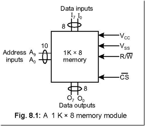
12. Diagrammatically show a 1 K × 8 memory,indicating the relevant pins.
Ans. The following figure shows the diagrammatic representation of a 1 K × 8 memory. ]
The memory will be selected only if CS (chip CS select) signal is low. 1 K represents 1024 memory 8 address locations so that 10 number of address O inputs (A0– A9) are required. I0– I7 and O0 – O7 (both 8 pins) represent respectively data inputs and outputs.
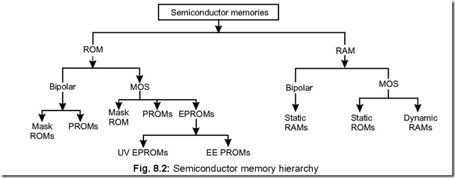
13. Show the different versions of semiconductor memories available.
Ans. Basically semiconductor memories can be RAM (Random Access Memory) or ROM (Read Only Memory)—both of which are available in bipolar technology or MOS (Metal Oxide Semiconductor) versions. The different versions available are:
14. What are the characteristic features of a RAM? Ans. The essential features of a RAM are:
1. It is volatile in nature—i.e., when the power is switched off, data stored at the different memory locations are totally lost.
2. When data/instruction is written at a memory location, previous data stored at this location is destroyed and replaced by the new data.
3. When data/instruction is read from an address location, the existing data is not lost (destroyed).
15. What is a CAM?
Ans. It stands for Content Addressable Memory. It is a special purpose RAM which performs association operation, in addition to read/write operations.
16. What is a PLA? What are the advantages of using a PLA?
Ans. A PLA stands for ‘Programmable Logic Array’. It is a non-volatile random access storage device. It can be used for implementing random logic circuitry and ROMs.
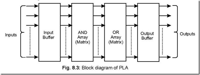
A PLA consists of two arrays (AND and OR), an input buffer and an output buffer.
The main advantages of using a PLA are: 1. Fastest access time 2. High switching
speed 3. Compact circuitry 4. Implementing random logic circuitry.
The block diagram of a PLA is as follows:
17. Applicationwise, write down the differences between RAM and ROM.
Ans. RAMs are used for writing/development of a program while ROMs are used for such programs which are repetitively required in a program—for example hexa-decimal conversion table, display program, time delay program and most importantly programmed instructions for system initialisation and operation.
18. What are the incompatibilities that may arise when memory devices are interfaced with mP? How are they removed?
Ans. The incompatibilities are: electrical, speed and bus.
Electrical incompatibility is removed by using bidirectional and unidirectional bus drivers.
Speed incompatibility is overcome by either slowing down the CPU clock or by
inserting wait states.
Bus incompatibility arises because of multiplexed address-cum-data bus, Read-Write signals differing for CPU and memory. The bus incompatibility can be removed by using extra hardware.
19. What are bit and byte organised memories?
Ans. For a 2n × m memory, where n is the number of address lines such that a maximum of 2n memory locations can be accessed and m is the word length, if m is 1 then the memory is said to be bit organised, whereas if m is 8, then the memory is said to be byte organised.
20. Mention the essential features of Mask programmable ROM and PROM. Ans. The essential features of these two are tabulated as follows:
Table 8.2: Comparison between mask programmable ROM and PROM
|
S. No. |
Mask programmable ROM |
PROM |
|
|
1. |
Manufactured by making special masks. |
1. |
Manufactured by blowing fusible |
|
nichrome wire links. |
|||
|
2. |
Programmed at the factory premises. |
2. |
Programmed by the user. |
|
3. |
No reprogramming possible. |
3. |
No reprogramming possible. |
|
4. |
Less costly. |
4. |
More costly. |
21. What is a EPROM? Mention its two types and compare.
Ans. EPROMs are manufactured with NMOSFET technology with an isolated gate structure.
There are two types of EPROM. These are:
UVEPROM : Ultraviolet erasable programmable Read-only-Memory EEPROM : Electrically erasable programmable Read-only-Memory (also known
as EAPROM)
A comparison between UVPROM and EEPROM is made hereunder:
Table 8.3: Comparison between EEPROM and UVPROM
|
S. No. |
EEPROM |
UVPROM |
|
|
1. |
Can be erased and programmed with |
1. |
Can be erased and programmed with |
|
electrical signals. |
ultraviolet light. |
||
|
2. |
The voltage on the floating gate structure |
2. |
The photo current from the insulated |
|
allows storage of information. |
gate structure allows storage of |
||
|
information. |
|||
|
3. |
Higher speed of operation. |
3. |
Lower speed of operation. |
|
4. |
More expensive. |
4. |
Less expensive. |
|
5. |
Relatively easy to manufacture. |
5. |
Relatively difficult to manufacture. |
|
6. |
Erasing takes several minutes. |
6. |
Erasing takes several minutes. |
|
7. |
In-situ erasing possible. |
7. |
In-situ erasing not possible. |
|
8. |
Byte wise erasing possible. |
8. |
Erasing wipes out the entire memory. |
|
9. |
Less packing density. |
9. |
More packing density. |
22. Name some of the application areas of ROM.
Ans. ROM has applications in many areas. Some of these are: bootstrap memory, firmware, data converters, function generators, data tables, etc.
23. What is a firmware?
Ans. A set of program/data must be made available to a microprocessor based system whenever it is powered on. This program/data is stored in ROM in what is called a firmware.
Laptop computers, PCs, etc. store their operating system programs and language interpreters (like PASCAL, BASIC, etc.) in ROM firmware.
24. What is a boot strap memory?
Ans. Most large computers store their operating system in external mass memory like
magnetic disk. For such computers, a small program, called the boot strap program, is stored in the ROM area of the computer. On powering such a computer, the bootstrap program is first executed which then loads the operating system programs from magnetic disk into the main (internal) memory of the computer. The OS is then run by the computer so that it becomes ready to accept user commands, this ‘start-up’ process is called ‘booting of the system’.
25. What is a flash memory?
Ans. This is an alternative to EPROMs and EEPROMs. It provides for very fast read access, in-circuit erasability. Its density almost matches that of EPROM, at the same time it is cost effective also. They consume less power and are able to withstand severe shock and vibration.
Most flash memory chips erase all the cells in the chip, although some newer version of flash memory chips has sectorwise erase option, i.e., 512 bytes of information can be erased at a time.
Typical values for memory write (per byte) are 10 ms, 100 ms and 5 ms for flash type, EPROM and EEPROM, respectively.
Flash memories are used in digital cellular phones, LAN switches, embedded
controllers, digital set-up boxes, etc.
26. What are the different types of SAMs?
Ans. SAM stands for Sequential Access Memory. Its different versions are: Shift Memory, Charged Coupled Devices (CCDs) and Bubble memories.
27. What kind of memory device is a CCD?
Ans. It is volatile type memory device, whose contents can be accessed in a serial manner.
28. Name the basic storage element in a CCD.
Ans. The basic storage element in a CCD is a MOS capacitor.
29. Mention the operations involved in a CCD memory. Ans. The main operations involved are:
z Converting a digital input signal into charge.
z Transferring the charges in a sequential manner.
z Charges at the outputs are converted back into digital form.
30. Discuss Bubble Memory.
Ans. Magnetic bubble memory is a solid state device. It is highly reliable, small in size, light in weight and its power consumption is low. Its access time is high—i.e., it is a slow device. A typical figure is 100 k bits/second.
In this type of memory, data is stored in magnetic bubbles. This is done in a thin film of magnetic material. A ‘1’ is represented by the presence of a bubble while the absence signifies a logical ‘0’.
It is a non-volatile semi random access type memory. Its readout is non-destructive in nature.
A bubble memory contains several loops, each loop of which contains a large number of bits. For read or write operation to be done, each loop possesses a 1-bit viewing window.
INTEL 7110 is a bubble memory chip having 1 M bits storage capacity while INTEL 7114 has a 4M bits capacity.
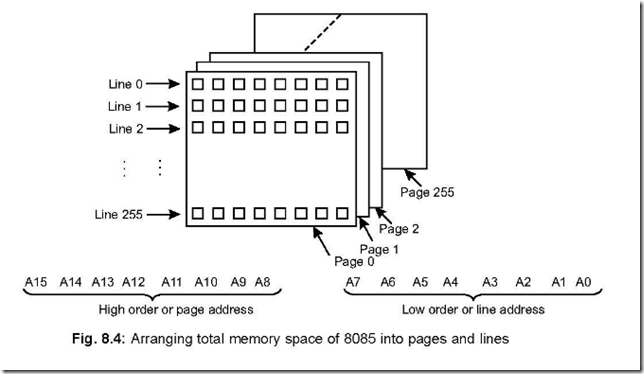
31. Explain how the entire addressable memory space of 8085 can be conceived of the pages of a book?
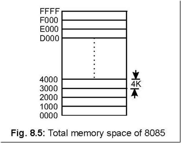
Ans. The entire addressable memory space is 216 = 65,536 lines, because 8085 has 16 address lines. This is arbitrarily divided into 256 pages (0 to 255 pages) with each page consisting of 256 lines (0 to 255 lines), as shown in Fig. 8.4
The sixteen address lines can be divided into higher (A15 – A8) and lower (A7 – A0) eight bits. On each page there are 256 lines defined by the lower byte (A7 – A0), while each page of the book is defined by the different combinations of the upper byte (A15 – A8).
The following figure shows an arbitrary but convenient way of showing the total
memory space, with each block consisting of 4 K lines i.e., 16 pages.
32. Mention the memory capacities corresponding to the number of address lines 10, 11, 12 16.
Ans. The memory capacities corresponding to the number of address lines 10, 11, … 15, 16 are 1 K, 2 K, 4 K, 8 K, 16 K, 32 K and 64 K, respectively.
33. What is a dual-port RAM? Mention its use.
Ans. It is a RAM having separate input and output pins. Because separate input and output pins are used (unlike normal RAM, in which data bus is bidirectional), it is used in high speed applications like the video RAM in a PC. In such a case the system bus feeds the RAM input with new informations while the video card reads from the RAM to constantly refresh the screen.
34. What is a NVRAM? Mention its use.
Ans. It stands for non-volatile RAM and is made by the combination of static RAM and an EEPROM. The memory structure of static RAM and EEPROM are mirror images of each other. When powered, NVRAM behaves as a normal RAM. When there is a power failure, RAM data is saved in EEPROM in less than 4 ms. On restoration of power, the reverse
![]() process occurs with contents of EEPROM sent back to RAM. Two pins STORE and
process occurs with contents of EEPROM sent back to RAM. Two pins STORE and
![]() RECALL of the NVRAM are used to store data in EEPROM and transfer it back to RAM respectively, both these transfers occurring on ‘low’ on the two pins.
RECALL of the NVRAM are used to store data in EEPROM and transfer it back to RAM respectively, both these transfers occurring on ‘low’ on the two pins.
The advantage of using an NVRAM is that a battery backup is not required to save
the RAM data in case of power failure.
The NVRAM finds its use in information storage such as time, date, monitor setting and other computer configurations.
35. What is a memory map?
Ans. A microcomputer system uses a mix of ROM, RAM for its addressable memory space.
Some of the memory space may be left unimplemented or open.
The memory map is a guide showing how the entire system memory has been allocated to ROM, RAM so that any future memory expansions can be executed effectively.
36. Draw a static RAM (SRAM) cell and explain its operation.
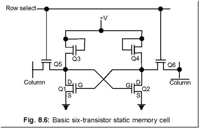
Ans. A standard SRAM consists of six transistors connected to form a R-S flip-flop. A SRAM cell is shown below. The transistors Q1 and Q2 form the cross-coupling transistors required for latching.
Data is written into the cell by applying the data and its complement at the column and column inputs respectively, with Q5 and Q6 in the ON condition. Data can be read
out from the column line after Q5 and Q6 are enabled.
Some of the characteristics of a SRAM cell are:
* It is volatile—i.e., data is lost on switch-off.
* When powered, the cell may assume either 1 or 0 state.
* Easy interfacing possible.
* No special timing circuits required.
* Bit density is low compared to DRAM.
37. Draw a dynamic RAM (DRAM) cell and explain its operation.
Ans. A basic DRAM storage cell is shown below:
When column (sense) and row (control) lines go high, the MOSFET conducts and charges the capacitor. Again when the column and row lines go high, the MOSFET opens and the capacitor retains its charge. Thus, it can store a single bit. Since only a single MOSFET and a capacitor are employed to store a bit, the DRAM density is high. Here, the MOS transistor acts as a switch.
Some of the characteristics of a DRAM cell are
* Higher packing density.
* Charge leaks, thus refreshing needed.
* Extra hardware needed to implement refreshing operation.
38. Compare a SRAM and DRAM cell.
Ans. The comparison is shown in a table 8.4:
Table 8.4: Comparison between Static and Dynamic RAM cells
|
S.No. |
Static memory |
Dynamic memory |
|
|
1. |
Stored data is retained as long as power |
1. |
Stored data gets lost and repeated |
|
remains ON. |
refreshing is required. |
||
|
2. |
Stored data do not change with time. |
2. |
Stored data changes with time. |
|
3. |
Consumes more power. |
3. |
Consumes less power than static |
|
memory. |
|||
|
4. |
Expensive. |
4. |
Less expensive. |
|
5. |
These memories have less packing density. |
5. |
Higher packing density. |
|
6. |
These memories are not easy to construct. |
6. |
Simpler in construction. |
|
7. |
No refreshing required and easy in operation. |
7. |
Refreshing required with additional |
|
memory circuitry and hence complicated |
|||
|
operation. |
|||
|
8. |
No maintenance. |
8. |
Maintenance needed. |
39. What are the different types of DRAMS available. Briefly describe their operations.
Ans. The different types of DRAMS available are as follows: SDRAM, FPM DRAM, EDO DRAM, DDRS DRAM, SL DRAM, and DR DRAM.
Here is a brief description about the different DRAMS.
SDRAM: It stands for synchronous DRAM. Internally, these DRAMs are organised into two banks for very fast reading. Its internal circuit is quite complex because of various operations needed such as burst length, sequential or interleaved data, self-refreshing,
CAS -before- RAS, etc.
SDRAMs transfer data in rapid-fire bursts of several sequential memory locations on the same page. The first memory accessing requires maximum time because of latency problem. After that data are transferred and clocked out by the bus system clock.
FPM DRAM: It stands for fast page mode DRAM. Within the same page it allows fast random memory accessing. Fast memory accessing is possible since to access memory locations on the same page, only the lower address lines are to be changed.
EDO DRAM: It stands for extended data output DRAM. It is a bit faster than FPM DRAM. In the case of EDO DRAM, the memory controller can output the next address while the current word is being read out from its output lines. This is not so in case of FPM DRAM.
DDRS DRAM: It stands for double data rate SD RAM.
The doubling of data rate over SDRAM is because of transfer of data on the rising and falling edge of the system clock.
SL DRAM: It stands for synchronous link DRAM.
It is an improvement over DDRS DRAM. Like DDRS DRAM, it also transfers data on the rising and falling edge of system clock with bus speed of around 200 MHz.
DR DRAM: It stands for Direct Rambus DRAM.
It is a proprietory of Rambus Inc. It utilises a newer approach to DRAM technology and is currently under development. Within this DR DRAM, more control has been incorporated for relisation of newer technology.
40. Why DRAM chips do not have CS signal?
Ans. The CS (chip select signal, normally low) signal either selects or deselects a chip as per
its status (0 selects and 1 deselects). DRAM chips have a (row address strobe) and a CAS (column address strobe), which together perform the function of CS signal.
Several address lines go to a row address decoder and several others go to a column address decoder. The output of these two decoders ( RAS and CAS ) then select a
particular cell of the corresponding row and column addresses in which read or write operation is then performed—like a static RAM.
41. What kinds of memory expansions are possible by combining memory chips?
Ans. By combining memory chips, two kinds of expansions are possible—one is word size expansion and the other is capacity expansion.
By word size expansion is meant that each memory location can be expanded say from 1 nibble to 1 byte, while by capacity expansion is meant the expansion of a 2 KB memory into, say a 8 KB or 16 KB memory unit.
42. What is the principle of operation of an optical memory?
Ans. An optical disk memory operates on the principle of reflection or scattering of a very narrow laser beam of the optical surface having microscopic size bubbles or pits. These represent logical 1’s.
43. What are the advantages of optical memory?
Ans. These kind of memories have large memory, relatively low in cost, very less dust-prone and access time comparable to hard disks.
44. Name the basic types of optical disk memories. Ans. The basic forms of optical disk memories are as follows:
* WORM or Write once read memory
*CD-ROM or Compact disk ROM
* OROM or Optical ROM
Out of the above, OROM can be written several times, while the contents of CD- ROMs and WORMs cannot be erased.
45. Name several commercially available EPROMs.
Ans. Several EPROMs are available commercially, which are listed below in a tabular form.
Out of these, the IC types 2708, 2716, 2732–although in use today, are increasingly being replaced by the newer varieties because of higher bit capacity.
|
ICs |
No. of bits (in K) |
Memory Organisation type |
Erasing type |
Output after erasing |
|
2708 |
8 |
1 K × 8 |
UV erasable |
FF H |
|
2716 |
16 |
2 K× 8 |
” |
” |
|
2732 |
32 |
4 K × 8 |
” |
” |
|
2764 |
64 |
8 K × 8 |
” |
” |
|
27128 |
128 |
16 K × 8 |
” |
” |
|
27256 |
256 |
32 K × 8 |
” |
” |
|
27512 |
512 |
64 K × 8 |
” |
” |
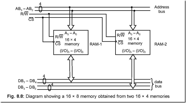
46. Design a memory having size 16 × 8 from 16 × 4 memory modules.
Ans. A 16 × 8 memory module indicates that it can address 16 different memory addresses, each address location can store 1 byte of data/instruction. The design is given below:
The address lines AB – AB can address 16 different addresses (from 0000 to 1111)
and connected to the two RAMs as shown. Chip selection is on the basis of CS signal
while R/W signal governs of whether reading (from memory) or writing (into the memory)
is to be done.
Once a particular address has been selected (by AB3 – AB0 lines), DB7 – DB4 stores the upper nibble of data in the left RAM (RAM-1) while DB3 – DB0 stores the lower nibble of the data in the right RAM (RAM-2).
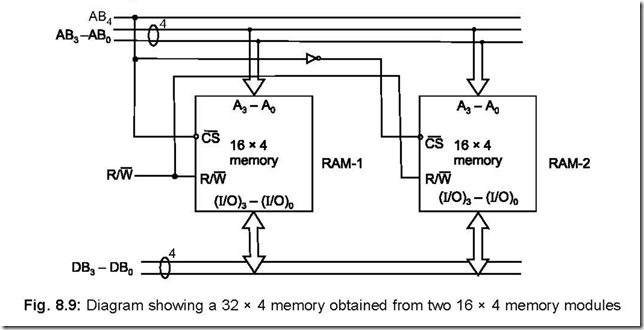
47. Develop a 32 × 4 memory module by combining two 16 × 4 memory chips.
Ans. The interconnections between the two 16 × 4 memory chips is shown below which yields a 32 × 4 memory module.
The address line AB4 selects either RAM-1 or RAM-2. RAM-1 is selected when AB4 = 0 while RAM-2 is selected when AB4 = 1. The address ranges for RAM-1 is 00000 to 01111 while the same for RAM-2 is 10000 to 11111. Thus the combination acts as a memory having 32 different addresses, each of which can store 1 nibble (4 bits) of data/ instruction—controlled by DB3 – DB0 lines.
48. Explain ‘memory foldback area’.
Ans. It can be explained with the help of µP 8085 which can address 64 KB. Out of the 16 address lines available, 3 address lines (say AB15 – AB13) can be inputted to a 3 to 8 line decoder (it may be 74ALS138). Thus each of the 8 output decoded lines divides the entire 64 K into 8 nos. of 8 K address blocks. Suppose in the 8 K address block 2000–3FFF, a single 2 K × 8 RAM is used intended for operation from 2000–27FF. Since this is a 2 KB of memory, it can be addressed by 11 address lines (say AB10 – AB0). Now since the decoder output is active for 8 K addresses, hence the RAM will also respond to the remaining 6K addresses—resulting in the same contents of RAM to appear at the three address blocks 2800–2FFF, 3000–37FF and 3800–3FFF. Thus, the areas of the memory (here 2800 to 3FFF —a 6 K block) which are redundantly occupied by a device because of incomplete address decoding is known as ‘memory foldback area’.
49. Mention the facilities available when power fails in a mC based system.
Ans. A ‘power-fail’ situation may occur at any time of a micro computer’s operations. Critical applications—such as in process control systems, intelligent terminals, printers demand a stand by power supply when the main power fails.
There are several methods by virtue of which critical data can be saved in power fail situations. These are:
1. Back up batteries can hold critical data in RAMs when power fails, but problem arises if power remains off for a considerable time, i.e., the back up batteries are drained out after prolonged use and data will be lost.
2. Sometimes critical data are stored in non-volatile flash memories—thus no battery back up is needed. Thus in this case no problem is there even if power remains off for a considerable time. But the associated problem of a flash chip remains—i.e., erasing or writing one or few bytes is not possible, rather it is done sectorwise at a time.
3. The third approach involves storing of all critical data in high speed RAMs. When power fails, the CPU executes a short power down program stored in ROM. This allows the critical data from high speed RAMs to CMOS RAMs which are provided with battery back up. The ‘power down program’ is invoked by a circuit that senses the power failure situation.
On restoration of power, the CPU executes a power up program so that all critical data stored in back up devices are transferred back to system RAM—This is true for the above mentioned three cases.
50. Draw a typical memory read cycle and explain.
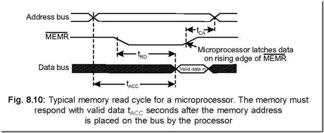
Ans. A typical memory read cycle is shown in Fig. 8.10.
The memory read cycle begins by outputting a valid address on its A0 – A15 address lines, after which the MEMR (active low) signal goes low, indicating that it is a memory read cycle. Then the microprocessor turns its internal data bus around so that it is now ready to receive data from the designated memory address.
The memory then places valid data on the data bus before the rising edge of MEMR . On the rising edge of the MEMR signal, the data is latched into the microprocessor signalling the end of the memory read cycle.
The three time periods shown in the figure are explained here.
tACC : This is the address access time. It corresponds to the maximum amount of time the memory needs to decode the address and place the selected data byte on the data bus.
tRD : This is the maximum amount of time after MEMR goes low that valid data is placed on the data bus by the designated memory.
tCA : This is the minimum amount of time after MEMR goes high before a new address appears on the address bus. If this minimum time is not met, it may be possible that a new memory address have started to put a new data byte on the data bus while the previous memory address was still outputting its own data. This will result in ‘bus contention’.
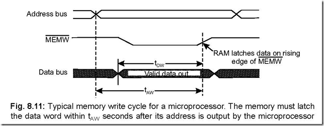
51. Draw a typical memory write cycle and explain. Ans. A typical memory write cycle is shown below:
The memory write cycle begins by outputting a valid address on its A0 – A15 address lines. Valid data is outputted on D7 – D0 lines early in the machine cycle which
corresponds to ‘data write set up time’. After this, the MEMW line goes low indicating
the memory write cycle.
The memory now has time up to the rising edge of MEMW to latch the data.
The two time periods shown in the figure are explained here.t : This is the minimum amount of time that valid address will be held on the bus
53. Explain the working of a FIFO (first in first out) memory system.
Ans. In a RAM FIFO, the data word which is entered first is the one which is read out first.
The FIFO memory operation (reading or writing) is controlled by a address pointer register that keeps a track of location where from data are to be written and also the location where from data are to be read.
A FIFO RAM is used as a data rate buffer and is really useful for situations where
data takes place at widely diverging rates—e.g., from a computer to a printer or a
keyboard to the computer. In case of printing, data meant for printing are first stored
in a FIFO memory inside the printer. The printer then reads out the FIFO memory at
its own rate and printing done in the same order in which they were sent by the
computer.
Data rate buffers are also known as linear buffers.
54. How do circular buffers differ from linear buffers?
Ans. A circular buffer is a memory system which stores the ‘last’ n values entered, where n is the number of memory locations in the buffer.
A circular buffer, whose memory capacity is n, is addressed by a mod-n address counter. Thus, when the mod-n counter reaches the last (or highest) memory location, the next one to be addressed by the same would be the first address location.
Digital signal processing and digital filtering employ circular buffers as memory because their calculations are based on the recently taken data values.
55. What is usually meant by the speed of a memory?
Ans. Usually, the term ‘speed of a memory’ is meant the time needed to access the memory.
This is also known as ‘access time’.
56. Why it is necessary to decode an address from the microprocessor?
Ans. The address (to either memory or I/O device) is given out by the microprocessor. It is to be remembered that microprocessor is a sequential device—meaning that it can communicate (read or write) with only one device at any given instant. This is because the data bus, address bus and the control bus for all the devices connected to the microprocessor are common. Thus to communicate properly with a device (either memory or I/O), decoding of address is a must. Thus address decoding pinpoints a particular memory location or I/O.
57. What are the common address decoding techniques?
Ans. There are two kinds of address decoding techniques. These are
z Absolute Decoding—also known as Full Decoding.
z Linear Decoding—also known as Partial Decoding.
58. Describe the absolute decoding scheme.
Ans. In this scheme, all the higher order address lines are decoded to select the memory chips and a particular memory chip is selected only for a specified logic level on these address lines. The particular memory chip is not selected for any other logic level. The three higher order address lines go to the decoder 74LS138 which outputs Y0 …. Y7. While a low on Y0 selects only RAM-1, a low on Y7 selects RAM-8. Thus depending on the address line status on A15 – A13, only one memory chip is selected.
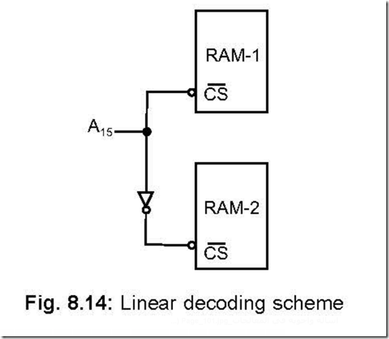
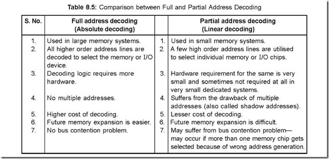
59. Describe the linear decoding scheme.
Ans. In this scheme, the decoder logic is eliminated by using individual high order address lines to select particular memory chip. As shown in the figure, when A15 = 1, ROM-2 is selected while RAM-1 is selected for A15 = 0.
60. Compare absolute and linear decoding schemes.
Ans. The comparison between the two schemes are tabulated below in Table 8.5:
Address Decoding
|
S. o. |
Full address decoding (Absolute decoding) |
Partial address decoding (Linear decoding) |
|
|
1. |
Used in large memory systems. |
1. |
Used in small memory systems. |
|
2. |
All higher order address lines are |
2. |
A few high order address lines are utilised |
|
decoded to select the memory or I/O |
to select individual memory or I/O chips. |
||
|
device. |
|||
|
3. |
Decoding logic requires more |
3. |
Hardware requirement for the same is very |
|
hardware. |
small and sometimes not required at all in |
||
|
very small dedicated systems. |
|||
|
4. |
No multiple addresses. |
4. |
Suffers from the drawback of multiple |
|
addresses (also called shadow addresses). |
|||
|
5. |
Higher cost of decoing. |
5. |
Lesser cost of decoding. |
|
6. |
Future memory expansion is easier. |
6. |
Future memory expansion is difficult. |
|
7. |
No bus contention problem. |
7. |
May suffer from bus contention problem— |
|
may occur if more than one memory chip gets |
|||
|
selected because of wrong address generation. |
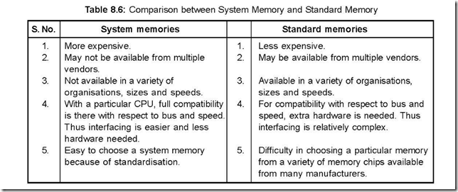
61. What are meant by system memories and standard memories?
Ans. Some CPU manufacturers design memory chips compatible with their CPUs. This is done to reduce burden on extra hardware. Such memories are called system memories.
Again so many memory chips are manufactured which can be used with different
varieties of CPUs after overcoming the incompatibility problems. Such memories are called standard memories.
62. Compare system memories with standard memories.
Ans. The comparison between system memories and standard memories is tabulated below:
Table 8.6: Comparison between System Memory and Standard Memory
|
S. No. |
System memories |
Standard memories |
|
|
1. |
More expensive. |
1. |
Less expensive. |
|
2. |
May not be available from multiple |
2. |
May be available from multiple vendors. |
|
vendors. |
|||
|
3. |
Not available in a variety of |
3. |
Available in a variety of organisations, |
|
organisations, sizes and speeds. |
sizes and speeds. |
||
|
4. |
With a particular CPU, full compatibility |
4. |
For compatibility with respect to bus and |
|
is there with respect to bus and speed. |
speed, extra hardware is needed. Thus |
||
|
Thus interfacing is easier and less |
interfacing is relatively complex. |
||
|
hardware needed. |
|||
|
5. |
Easy to choose a system memory |
5. |
Difficulty in choosing a particular memory |
|
because of standardisation. |
from a variety of memory chips available |
||
|
from many manufacturers. |
63. What is the advantage of memory interlacing technique? Ans. It increases the effective speed of memory.
64. What advantage is derived when larger RAM is inserted in a mC based system? Ans. It enhances speed by eliminating the need for external memory.
