Principles of switching circuits
DC–DC converters
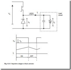
The simplest and most common dc–dc converter is the step-down chopper or buck converter, and is shown in Fig. 11.11 along with idealized waveforms. The circuit operates from a dc source, Vin, and supplies power at a lower voltage, Vo, to a load element, which is shown here as a resistor in parallel with a smoothing capacitor, but could
instead be the armature of a dc motor, as described in section 10.10.1. The inductor acts as an energy storage buffer between the input and the output.
When the transistor is switched on the voltage VD is equal to Vin, the freewheel diode is reverse biased, and a voltage of Vin – Vo drives a linearly increasing current, IL, through the inductor. When the transistor turns off, the inductor current diverts to the freewheel diode, voltage VD is zero and there is a reverse voltage of Vo across the inductor resulting in a linear fall in current. The load voltage Vo is equal to the aver- age of the VD waveform since no average or dc voltage is dropped across an ideal inductor, and is given by eqn 11.8:
where D is the duty ratio or on time-to-period ratio of the transistor, and 0 £ D £ 1.
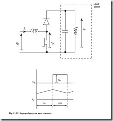
The step-up chopper or boost converter (Fig. 11.12) is essentially a circuit dual of the buck converter. The transistor and diode again conduct the inductor current alternately. The inductor current rises linearly when the transistor is turned on, the inductor voltage being equal to Vin, and the current falls linearly when the transistor is turned off since the inductor voltage is then reversed with a value of Vo – Vin.
The average of the VD waveform is now equal to the input voltage, and since the average of VD is Vo(1-D), the output voltage may be expressed in eqn 11.9:
which confirms the voltage step-up operating characteristics of the circuit.
Two- and four-quadrant converters
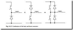
By re-drawing the boost converter circuit with the input on the right, the buck and boost circuits may be combined to form the bidirectional converter shown in Fig. 11.3. To ensure proper circuit operation the transistors must be switched in anti-phase. With a dc source connected to the left hand terminals of the bidirectional converter and a load element on the right, the circuit operates as a buck converter and the inductor current flows to the right. If the dc source is connected to the right hand terminals and the load connected on the left, the inductor current will be reversed and the circuit will operate as a boost converter.
The circuit therefore provides two-quadrant operation with unidirectional voltage at both terminals, but bidirectional currents. The circuit could be used to control the charging and discharging of a battery, or to provide two-quadrant operation of a dc machine, with unidirectional voltage and therefore speed, but with bidirectional cur- rent and torque. The bidirectional converter in Fig. 11.13 is commonly referred to as an inverter leg since it forms the building block of dc–ac inverter circuits.
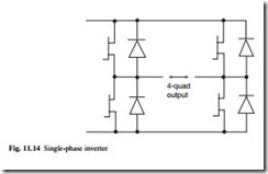
To achieve a four-quadrant output, two of the bidirectional circuits operating from a common dc source may be combined as shown in Fig. 11.14. The inductor is no longer shown but it is implied and it might typically be formed from the load impedance, such as the inductance of a motor.
The four-quadrant output is formed by the difference of the two bidirectional converter outputs. The resultant circuit is sometimes known as an H-bridge or a single- phase inverter, and it has a wide variety of applications, requiring different operating patterns for the transistors. The transistors in each leg of the circuit would normally be
operated in anti-phase to ensure that the leg output voltages are always defined by the state of the transistors. Typical applications include:
● four-quadrant drive for a dc machine, enabling motoring and generating operation with both forward and reverse rotation, as described in section 10.10.1. Diagonally opposite transistors could be operated in synchronism with variable duty ratio. With a duty ratio of 0.5 the average machine voltage would be zero, and increasing or decreasing the duty ratio could produce positive or negative average voltages.
● high frequency ac output to drive a high-frequency transformer in a switched- mode power supply. Here the two legs could each be operated with 0.5 duty ratios, and a variable phase shift introduced between the legs to produce a controllable quasi-squarewave output voltage.
● synthesizing an ac output from a dc source, for example to supply ac equipment in the absence of a utility connection, or to interface a dc energy source such as a photovoltaic array with utility. In this case, diagonally opposite devices could be operated in synchronism with a 0.5 duty ratio, producing a squarewave ac output voltage, however, a filter circuit may be required to remove the unwanted harmonics from the squarewave. Alternatively, the devices could be operated at
a much higher frequency than the utility using sinusoidal pulse width modulation techniques, discussed in section 11.4.4.
Since the single-phase inverter produces a four-quadrant output, it can not only be used to synthesize an ac output from a dc power source, but can also be used to control the flow of power from an ac source to a dc load. If sinusoidal PWM techniques are used, then it is known as a PWM rectifier.
Three-phase inverter
To synthesize a set of three-phase voltages from a dc source, three inverter legs are connected together as shown in Fig. 11.15. The circuit has two operating modes, either the transistors operate at the same frequency as the ac output waveforms, known as quasi-squarewave or six-step operation, or alternatively the devices operate at a much higher frequency than the ac output using a form of sinusoidal pulse width modulation.
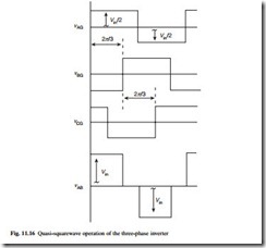
Figure 11.16 illustrates the simpler quasi-squarewave operation of the three-phase inverter. The transistors in each leg operate in anti-phase with duty ratios of 0.5, the leg output voltages, measured with respect to a notional ground at the mid-point of the dc input, are therefore symmetrical squarewaves of ± Vin /2. By displacing the switching actions in the three legs by 2p/3 radians or 120° as shown, the resultant line- to-line output voltages form a set of mutually displaced quasi-squarewaves. The VAB line-to-line voltage is shown as an example and consists of 120° intervals of positive and negative voltage separated by 60° intervals of zero voltage. Since the line-to-line output voltages are identical in form to the ideal input currents drawn by the six-pulse rectifier (Fig. 11.2) the waveforms will also have an identical frequency spectrum (Fig. 11.5), the non-zero harmonics being of order 6k ± 1. From eqn 11.3 the amplitude of the fundamental component of the line-to-line waveforms.
One of the largest application areas for the three-phase inverter is in variable speed drive systems for ac motors, as described in section 10.10.2.
Sinusoidal Pulse Width Modulation (PWM)
The most common operating mode for inverter circuits is with the transistors switching at a much higher frequency than the ac output waveform that is being synthesized, typically twenty times greater or more, which implies switching frequencies in the region of 1–20 kHz for a mains frequency inverter. The duty ratio of the transistors is varied throughout the mains cycle to shape the required sinusoidal output voltage. The main advantage of Pulse Width Modulation (PWM) methods for inverter control is the harmonic purity of the output waveform. Apart from the required fundamental component, the frequency spectrum of the output contains only switching frequency- related harmonics, and these are at high frequency, typically clustered around integer multiples of the switching frequency. These frequency components may be removed by a small high frequency filter if necessary, however, the load impedance itself often acts as a low pass filter, making additional filtering unnecessary.
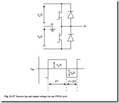
The basic principle of PWM control is explained with reference to the single inverter leg in Fig. 11.17. The leg output voltage nAG is shown with respect to a notional ground at the mid-point of the dc supply. The transistors operate in anti-phase with switching period T, the upper device having a duty ratio or on time-to-period ratio D,
and the lower device therefore having a duty ratio of (1-D). The local average, n-AG, of the nAG waveform, taken across the arbitrary switching cycle in Fig. 11.17 is given by eqn 11.10:
By varying D from one cycle to the next, the local average of nAG may be forced to follow a required waveform and to synthesize a sinusoidal output waveform, the duty ratio should be varied according to eqn 11.11,
where w is the angular frequency of the waveform to be synthesized, and the parameter M is known as the depth of modulation or the modulation index. With a modulation index of zero the duty ratio will be constant, whilst a modulation index of unity will result in the duty ratio varying over the full range of 0 £ D £ 1. Substituting eqn 11.11 into eqn 11.10 gives the local average output voltage in eqn 11.12,
which has the required sinusoidal form, the amplitude being (Vin/2)M. The modulation index therefore controls the amplitude of the synthesized output.
Equation 11.12 shows that with a modulation index of unity the amplitude of the output waveform is limited to Vin/2. A modulation index of greater than unity, known as over-modulation, allows the amplitude of the fundamental component of the output to be increased, although eqn 11.12 breaks down in this region. However, over-modulation has the disadvantage of introducing low-order harmonics in the output spectrum. Alternatively the technique of third harmonic injection may be used to increase the amplitude of the fundamental component of the output by around 15 per cent without degrading the frequency spectrum. This is achieved by adding a small amount of third harmonic to the modulating waveform. The addition of the third harmonic does not affect the line-to-line output waveforms of a three-phase inverter since the third harmonic is a common mode component in three-phase systems.
A variety of methods have been developed for the practical implementation of sinusoidal PWM and the determination of the required duty ratio variation. Naturally sampled PWM is intuitively the most simple, and involves comparing the sinusoidal modulating waveform with a triangular carrier signal at the switching frequency. The analogue implementation of this technique is fraught with offset and drift problems, and, being analogue in nature, the method does not readily lend itself to digital implementations. Instead, methods such as regularly sampled PWM have been developed, which use sample and hold techniques to simplify the calculations within a processor. Most recently, the method of space vector PWM has become common for three-phase inverters. This uses a single rotating vector to represent the required three-phase output waveforms, and the transistor switching patterns for each of the three legs are calculated simultaneously, resulting in a very efficient implementation, furthermore the third harmonic injection to increase the maximum fundamental output is inherently provided.
