Power electronic components
Power electronic components are semiconductor devices, such as diodes, thyristors, transistors, etc. that are used in the power circuit of a converter. In power electronics, they are used in the non-linear switching mode (on/off mode) and not as linear amplifiers. In other words, these devices behave like an electronic switch.
An electronic switch electronically connects or disconnects an AC or DC circuit and can usually be switched ON and/or OFF. Conduction is usually permitted in one direction only.
The following components are devices that are commonly used as electronic switches in power electronic converters. Developments in semiconductor technology have made these power electronic components smaller, more reliable, more efficient (lower losses), cheaper, and able to operate at much higher voltages, currents, and frequencies. The idealized operating principles of these components can be described in terms of simple mathematical expressions.
• Power diodes
• Power thyristors
• GTO
• MOS-controlled thyristors (MCT)
• Power bipolar junction transistors (BJT)
• Field effect transistors (FET, MOSFET)
• Insulated gate bipolar transistor (IGBT)
• Resistors (provide resistance)
• Reactors or chokes (provide inductance)
• Capacitors (provide capacitance).
Power diodes
A power diode is a semiconductor power on/off switch that allows flow of current in one direction, depending upon its connection. It is a two-terminal semiconductor device.
The two terminals of a diode are called the anode (A) and the cathode (K). These names are derived from the days when valves were commonly used.
Construction-wise, it has a single P–N junction. It consists of a two-layer silicon wafer attached to a substantial copper base. The base acts as a heat sink, a support for the enclosure and one of the electrical terminals of the diode. The other surface of the wafer is connected to the other electrical terminal. The enclosure seals the silicon wafer from the atmosphere and provides adequate insulation between the two terminals of the diode.
• Forward conduction: Resistance less
• Reverse blocking: Loss less
• Switch on/off time: Instantaneous.
It is forward-biased, when the anode is positive, relative to the cathode and the diode conducts current, i.e., the switch is closed. It is reverse-biased, when the anode is negative, relative to the cathode and the flow of the current is blocked, i.e., the switch is open. This ability of the diode, to block the current flow in one direction, makes it suitable for rectifier applications, where it is required to allow the current flow in one direction only.
Depending on the application requirements, the following types of diodes are available:
Schottky diodes These diodes are used where a low forward voltage drop, typically 0.4 V, is needed for low output voltage circuits. These diodes have a limited blocking voltage capability of 50–100 V.
Fast recovery diodes These diodes are designed for use in circuits where fast recovery times are required, for example, in combination with controllable switches in high- frequency circuits. Such diodes have a recovery time (tRR) of less than a few microseconds.
Line-frequency diodes The on-state voltage of these diodes is designed to be as low as possible to ensure that they switch on quickly in rectifier bridge applications. Unfortunately, the recovery time (tRR) is long, but this is acceptable for line-frequency rectifier applications. These diodes are available with blocking voltage ratings of several kV and current ratings of several hundred kA. In addition, they can be connected in series or parallel to satisfy high-voltage or current requirements.
Power thyristors
Thyristors are sometimes referred to as SCR (silicon-controlled rectifiers). This was the name originally given to the device when it was invented by General Electric (USA) in around 1957. However, this name has never been universally accepted and used.
The name thyristor, is a generic term, that is applied to a family of semiconductor devices that have regenerative switching characteristics. There are many devices in the Thyristor family including the power thyristor, the GTO, the field controlled thyristor (FCT), the Triac, etc. It has two power terminals, called the anode (A) and the cathode (K), similar to a diode, and a third control terminal called the Gate (G), which is used to control the firing of the thyristor.
It is operationally similar to a diode, except that it requires a momentary positive voltage pulse, at the gate terminal, for conduction when connected in forward bias. A thyristor consists of a four-layer silicon wafer with three P–N junctions. High-voltage, high-power thyristors sometimes also have a fourth terminal, called an auxiliary cathode. This is used for connection to the triggering circuit. This prevents the main circuit from interfering with the gate circuit.
A thyristor is very similar to a power diode in both physical appearance and construction, except that the gate terminal is required to trigger the thyristor into a conduction mode.
The thyristor is turned off when it becomes reverse-biased and/or the forward current falls below the holding current. This must be controlled externally in the power circuit. Most SCRs have a heat sink for dissipating the heat generated during the operation.
Triacs
This is a different device from the thyristors category. Construction-wise, two SCRs are connected anti-parallel with each other. SCR conducts in a forward direction only, but Triac conducts in both directions. Therefore, if the output of a diode is a DC current when connected in an AC circuit, the output of a Triac is an AC current instead of a DC current. Triac has three terminals named MT1, MT2, and Gate. Triac can conduct in any direction with the gate pulse, either positive or negative. Triac can be used to vary the average AC voltage going to a load by changing the firing angle.
Gate-controlled power electronic devices
A number of gate-controlled devices have become available in the past decade. These are suitable for use as bi-stable switches on power inverters for AC VSDs. These can be divided into the following two main groups of components:
• Those based on Thyristor technology such as GTO and FCT
• Those based on Transistor technology such as the BJT, FET, and the insulated gate bipolar transistor (IGBT).
Gate turn-off thyristor (GTO)
A GTO thyristor is another member of the thyristor family. It is very similar in appearance and performance to a normal thyristor, with an important additional feature being that it can be turned off by applying a negative current pulse to the gate. GTO thyristors have high current and voltage capability and are commonly used for larger converters. This is especially true when self-commutation is required.
• Forward conduction: Resistance less
• Forward blocking: Loss less (no leakage current)
• Reverse blocking: Loss less (no leakage current)
• Switch on/off time: Instantaneous.
The performance of a GTO is similar to a normal thyristor. Forward conduction is blocked until a positive pulse is applied to the gate terminal. When the GTO has been turned on, it behaves like a thyristor and continues to conduct even after the gate pulse is removed, if the current is higher than the holding current. The GTO has a higher forward voltage drop of typically 3–5 V. The latching and the holding currents are also slightly higher.
The important difference is that the GTO may be turned off by a negative current pulse applied to the gate terminal. This important feature permits the GTO to be used in self- commutated inverter circuits. The magnitude of the off pulse is large and depends on the magnitude of the current in the power circuit. Typically, the gate current must be 20% of the anode current. Consequently, the triggering circuit must be quite large and this results in additional commutation losses. Like a thyristor, conduction is blocked in the reverse- biased direction or if the holding current falls below a certain level.
Since the GTO is a special type of thyristor, most of the other characteristics of a thyristor covered above also apply to the GTO. The mechanical construction of a GTO is very similar to a normal thyristor with stud types common for smaller units and disk types common for larger units. GTO thyristors are usually used for high-voltage and current applications and are more robust and tolerant to over-current and over-voltages than power transistors. GTOs are available for ratings of up to 2500 A and 4500 V. The main disadvantages are the high gate current required to turn the GTO off and the high forward volt drop.
Field controlled thyristors (FCT)
Although the GTO is likely to maintain its dominance for high-power, self-commutated converter applications for some time, new types of thyristors are under development in which the gate is voltage-controlled. The turn-on is controlled by applying a positive voltage signal to the gate and the turn-off by a negative voltage. Such a device is called a FCT. The name affects the similarity to the FET. The FCT is expected to eventually supersede the GTO because it has a simple control circuit in which both the cost and the losses can be substantially reduced.
Power bipolar junction transistors (BJT)
Transistors have traditionally been used as amplification devices, where control of the base current is used to make the transistor conductive to a greater or a lesser degree. Until recently, they were not widely used for power electronic applications.
The main reasons were because the control and protective circuits were considerably more complicated and expensive, and transistors were unavailable for high-power applications. They also lacked the overload capacity of a thyristor and to protect transistors with fuses was unfeasible.
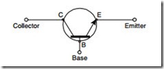
The NPN transistor, known as a BJT, is a cost-effective device for use in power electronic converters. Modern BJTs are usually supplied in an encapsulated module and
each BJT has two power terminals, called the collector (C) and an emitter (E), and a third control terminal called the base (B).
A transistor is not inherently a bi-stable (on/off) device. To make a transistor suitable for conditions in a power electronic circuit where it is required to switch from the blocking state (high voltage, low current) to the conducting state (low voltage, high current) it must be used in its extreme conditions – fully off to fully on. This potentially stresses the transistor and the trigger, and protective circuits must be coordinated, to ensure the transistor is not permitted to operate outside its safe operating area. Forward conduction is blocked until a positive current is applied to the gate terminal and it conducts as long as a voltage is applied. During forward conduction, it also exhibits a forward voltage drop, which causes losses in the power circuit. The BJT may be turned off by applying a negative current to the gate.
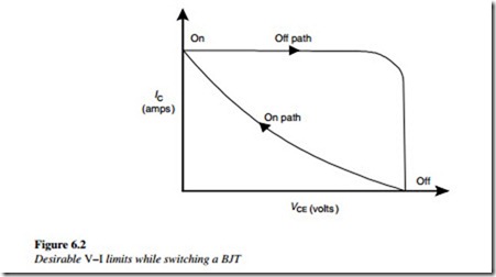
Suitable control and protective circuits have been developed to protect the transistor against over-current when it is turned on and against over-voltage when it is turned off
(Figure 6.2). When turned on, the control circuit must ensure that the transistor does not come out of saturation, otherwise; it will be required to dissipate a high power. In practice, the control system has proved to be cost effective, efficient, and reliable in service.
The following are the advantages of BJT as a switch:
• Requires very low driving voltages
• Can operate at very high speed
• Can be turned on and off from the base terminal, which makes them suitable for self-commutated inverter circuits
• Good power handling capabilities
• Low forward conduction voltage drop.
The following are the disadvantages of BJT as a switch:
• Considered less robust and less tolerant of overloads and ‘spikes’ than thyristors
• Do not tolerate reverse voltages
• Relatively slow switching times compared with other devices
• Inferior safe operating area
• Has complex current-controlled gate driver requirements.
GTO thyristors are often preferred for converters. When BJTs are used in inverter bridges, they must be protected against high reverse voltages, by means of a reverse diode in series or in parallel. For the same reason, transistors are not used in rectifier bridges that have to be able to withstand reverse voltages.
The base amplification factor of a transistor is fairly low (usually 5–10 times). The trigger circuit of the transistor, consequently, must be driven by an auxiliary transistor to
reduce the magnitude of the base trigger current required from the control circuit. To perform this, the Darlington connection is used.
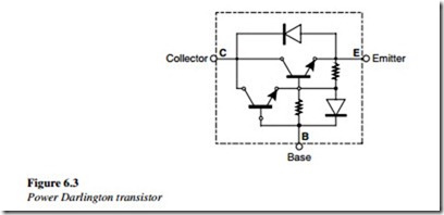
Figure 6.3 shows a double Darlington connection, but for high-power applications, two auxiliary transistors (triple Darlington) may be used in cascade to achieve the required amplification factor. The overall amplification factor is approximately the product of the amplification factors of the two (or three) transistors.
Transistors, used in VSD applications, are usually manufactured as an integrated circuit and encapsulated into a three-terminal module, complete with the other necessary components, such as the resistors and an anti-parallel protection diode. The module has an insulated base suitable for direct mounting onto the heat sink. This type of module is sometimes called a Power Darlington transistor module.
As shown in Figure 6.3, the anti-parallel diode protects the transistors from reverse biasing. In practice, this diode in the integrated construction is slow and may not be fast
enough for inverter applications. Consequently, converter manufacturers sometimes use an external fast diode to protect the transistors. Power BJT are available for ratings of up to a maximum of about 300 A and 1400 V. For VSDs that require a higher power rating, GTOs are usually used in the inverter circuit.
Field effect transistor (FET)
BJT is a current-driven device. The current flows through the base controls and the flow of current is between the collector and the emitter. The FET Gate is voltage-controlled. FET is a special type of transistor that is particularly suitable for high-speed switching applications.
Its main advantage is that its Gate is voltage-controlled rather than current-controlled. It behaves like a voltage-controlled resistance with the capacity for high-frequency performance.
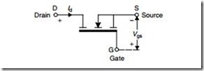
FETs are available in a special construction known as the MOSFET. MOS stands for metal oxide silicon. The MOSFET is a three-terminal device with terminals called the source (S), the drain (D), and the gate (G), corresponding to the emitter, collector, and gate of the NPN transistor.
• Forward conduction: Resistance less
• Forward blocking: Loss less (no leakage current)
• Reverse blocking: Loss less (no leakage current)
• Switch on/off time: Instantaneous.
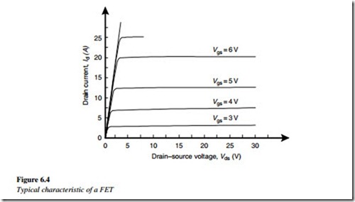
The overall performance of an FET is similar to a power transistor, except that the gate is voltage-controlled. Forward conduction is blocked if the gate voltage is low, typically less than 2 V. When a positive voltage Vgs is applied to the gate terminal, the FET conducts and the current rises in the FET to a level dependent on the gate voltage. The FET will conduct as long as a gate voltage is applied. The FET can be turned off by removing the voltage applied to the gate terminal or by making it negative.
MOSFETs are majority carrier devices, so they do not suffer from long switching times. With their very short switching times, the switching losses are low. Consequently, they
are best suited to high-frequency switching applications. A typical performance characteristic of a FET is shown in Figure 6.4.
Initially, high-speed switching was not an important requirement for AC converter applications. With the development of PWM inverters, high-frequency switching has become a desirable feature to provide a smooth output current waveform. Consequently, power FETs were not widely used until recently.
At present, FETs are only used for small PWM frequency converters. The ratings are available from about 100 A at 50 V to 5 A at 1000 V, but for VSD applications, MOSFETs need to be in the 300–600 V range. The advantages and disadvantages of MOSFETs are almost exactly the opposite of BJTs.
The main advantages of a power MOSFET are given below:
• High speed switching capability (10–100 ns)
• Relatively simple protection circuits
• Relatively simple voltage-controlled gate driver with low gate current. The main disadvantages of a power MOSFET are given below:
• Relatively low power handling capabilities
• Relatively high forward voltage drop, which results in higher losses than GTOs and BJTs, limits the use of MOSFETs for higher power applications.
Insulated gate bipolar transistor (IGBT)
The insulated gate bipolar transistor (IGBT) is an attempt to unite the best features of the BJT and the MOSFET technologies.
The construction of the IGBT is similar to a MOSFET with an additional layer to provide conductivity modulation, which is the reason for the low-conduction voltage of the power BJT.
The IGBT device has a good forward blocking but a very limited reverse blocking ability. It can operate at higher current densities than either a BJT or MOSFET by allowing a smaller chip size.
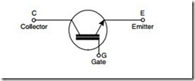
The IGBT is a three-terminal device. The power terminals are called the emitter (E) and the collector (C), using the BJT terminology, while the control terminal is called the gate
• Forward conduction: Resistance less
• Forward blocking: Loss less (no leakage current)
• Reverse blocking: Loss less (no leakage current)
• Switch on/off time: Instantaneous.
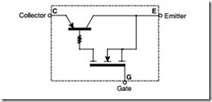
The electrical equivalent circuit of the IGBT shows that the IGBT can be considered as a hybrid device, similar to a Darlington transistor configuration, with a MOSFET driver, and a power bipolar PNP transistor. Although the circuit symbol above suggests that the device is related to a NPN transistor, this should not be taken too literally.
The gate input characteristics and gate drive requirements are very similar to those of a power MOSFET. The threshold voltage is typically 4 V. Turn-on requires 10–15 V and takes about 1 µs. The turn-off takes about 2 µs and can be obtained by applying 0 V to the gate terminal. The turn-off time can be accelerated, when necessary, by using a negative drive voltage. IGBT devices can be produced with faster switching times at the expense of an increased forward voltage drop.
IGBTs are currently available in ratings from a few amps to around 500 A at 1500 V, which are suitable for three-phase AC VSDs rated up to about 500 kW at 380 V/ 415 V/480 V. They can be used at switching frequencies up to 100 kHz. BJTs have now largely been replaced by IGBTs for AC VSDs.
The following are the main advantages of the insulated gate bipolar transistor (IGBT):
• Good power-handling capabilities
• Low forward conduction voltage drops of 2–3 V, which is higher than for BJT but lower than for a MOSFET of similar rating
• This voltage increases with temperature making the device easy to operate in parallel without danger of thermal instability
• High-speed switching capability
• Relatively simple voltage-controlled gate driver
• Low gate current.
Some other important features of the IGBT are given below:
• There is no secondary breakdown with the IGBT, giving a good safe operating area and low switching losses
• Only small snubbers are required
• The inter-electrode capacitances are not as relatively important as in a MOSFET, thus reducing Miller feedback.
There is no body diode in the IGBT, as with the MOSFET, and a separate diode must be added in anti-parallel when a reverse conduction is required, for example, in voltage source inverters


