Objectives
After studying this unit, the student will be able to:
• Discuss the atomic structure of conductors, insulators, and semiconductors
• Discuss how a P-type material is produced
Discuss how anN-type material is produced
Many of the control systems used in today ‘s industry are operated by solid-state devices as well as magnetic and mechanical devices. If an electri cian is to install and troubleshoot control systems, he must have an understanding of electronic con trol devices as well as relays and motor starters.
Solid-state devices, such as diodes and tran
sistors, are often referred to as semiconductors. The word, semiconductor, refers to the type of mate rial used to make solid-state devices. To under stand how solid-state devices operate, one must first study the atomic structure of conductors, in sulators, and semiconductors.
CONDUCTORS
Conductors are materials that provide easy paths for the flow of electrons. Conductors are generally made from materials that have large, heavy atoms. For this reason, most conductors are metals. The best electrical conductors are silver, copper and aluminum.
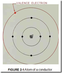
Conductors are also made from materials that have only one or two valence electrons in their at oms. (Valence electrons are the electrons in the outer orbit of an atom, figure 2-1.) An atom that has only one valence electron makes the best electrical conductor because the electron is held loosely in orbit and is easily given up for current flow.
INSULATORS
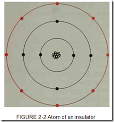
Insulators are generally made from light weight materials that have small atoms. The outer orbits of the atoms of insulating materials are filled or almost filled with valence electrons. This means an insulator will have seven or eight valence elec trons as in the example in figure 2-2. Since an in sulator has its outer orbit filled or almost filled with valence electrons, the electrons are held tightly in orbit and are not easily given up for cur rent flow.an insulator will have seven or eight valence elec trons as in the example in figure 2-2. Since an in sulator has its outer orbit filled or almost filled with valence electrons, the electrons are held tightly in orbit and are not easily given up for cur rent flow.
SEMICONDUCTORS
Semiconductors, as the word implies, are ma terials that are neither good conductors nor good insulators. Semiconductors are made from materials that have four valence electrons in their outer orbits, figure 2-3. Germanium and silicon are the most common semiconductor materials used in the electronics field. Of these materials, silicon is used more often because of its ability to withstand heat.
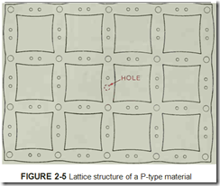
When semiconductor materials are refined into a pure form, the molecules arrange them selves into a crystal structure which has a definite pattern, figure 2-4. This type of pattern is called a lattice structure. A pure semiconductor material such as silicon has no special properties and will do little more than make a poor conductive mate rial. To make semiconductor material useful in the
production of solid-state components, it is mixed with an impurity. When pure semiconductor ma terial is mixed with an impurity that has only three valence electrons, such as indium or gallium, the lattice structure changes leaving a hole in the material, figure 2-5. This hole is caused by a miss ing electron. Since the material now lacks an elec tron, it is no longer electrically neutral. Electrons are negative particles. The hole, which has taken the place of an electron, has a positive charge; therefore, the semiconductor material now has a net positive charge and is called a P-type material.
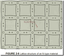
When a semiconductor material is mixed with an impurity that has five valence electrons, such as arsenic or antimony, the lattice structure has an excess of electrons, figure 2-6. Since electrons are negative particles, and there are more electrons in the material than there should be, the material has a net negative charge. This material is referred to as an N-type material because of its negative charge.
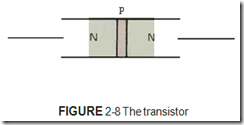
All solid-state devices are made from combi nations of P- and N-type materials. The type of device formed is determined by how the P- and N-type materials are connected. The number of layers of material and the thickness of each layer play an important part in determining what type of device is formed. For example, the diode is of ten called a PN junction because it is made by joining a piece of P-type material and a piece of N-type material, figure 2-7. The transistor, on the other hand, is made by joining three layers of semiconductor materials, figure 2-8.
REVIEW QUESTIONS
1. The atoms of a material used as a conductor generally contain ——————— valence electrons.
2. The atoms of a material used as an insulator generally contain——————— valence electrons.
3. The two materials most often used to produce semiconductor devices are
——————— and ———————
4. What is a lattice structure?
5. How is a P-type material made?
6. How is an N-type material made?
7. Which type of semiconductor material can withstand the greatest amount of heat?
All electronic components are formed from P-type and N-type materials. What factors determine the kind of components formed?
