Voltage regulators
Two factors can cause the output voltage of a power supply to vary. First, the input voltage to the power supply can vary, resulting in increases and decreases in the output voltage. Second, the load resistance can vary, resulting in a change in current demand.
Many circuits are designed to operate at a certain voltage. If the voltage varies, the operation of the circuit is affected. Therefore, the power supply must produce the same output regardless of load and input voltage changes. To accomplish this, a voltage regulator is added after the filter.
There are two basic types of voltage regulators: shunt voltage regulators and series voltage regulators. They are named for the method by which they are connected with the load. The shunt regulator is connected in parallel with the load, whereas the series regulator is connected in series with the load. Series regulators are more popular than shunt regulators because they are more efficient and dissipate less power. The shunt regulator also acts as a control de- vice, protecting the regulator from a short in the load.
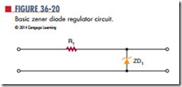
Figure 36-20 shows a basic zener diode regulator circuit. This is a shunt regulator. The zener diode is connected in series with a resistor. The input voltage, unregulated DC voltage, is applied across both the zener diode and the resistor so as to make the zener
diode reverse biased. The resistor allows a small cur- rent to flow to keep the zener diode in its zener breakdown region. The input voltage must be higher than the zener breakdown voltage of the diode. The voltage across the zener diode is equal to the zener diode’s voltage rating. The voltage dropped across the resistor is equal to the difference between the zener diode’s voltage and the input voltage.
The circuit shown in Figure 36-20 provides a constant output voltage for a changing input voltage. Any change in the voltage appears across the resistor. The sum of the voltage drops must equal the input voltage. By changing the output zener diode and the series resistor, the output voltage can be increased or decreased.
The load resistance and the output voltage deter- mine the current through the load. The load current and the zener current flow through the series resistor. The series resistor must be chosen carefully so that the zener current keeps the zener diode in the breakdown zone and allows the current to flow.
When the load current increases, the zener current decreases, and the load current and zener current together maintain a constant voltage. This allows the circuit to regulate for changes in output current as well as input voltage.
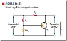
Figure 36-21 shows a shunt regulator circuit using a transistor. Note that transistor Q1 is in parallel with the load. This protects the regulator in case a short develops with the load. More complex shunt regulators are available that use more than one transistor.
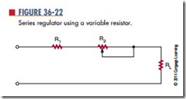
The series regulator is more popular than the shunt regulator. The simplest series regulator is a variable resistor in series with the load (Figure 36-22). The resistance is adjusted continuously to maintain a constant voltage across the load. When the DC voltage increases, the resistance increases, dropping more voltage. This maintains the voltage drop across the load by dropping the extra voltage across the series resistor.
The variable resistor can also compensate for changes in load current. If the load current increases, more volt- age drops across the variable resistor, which results in less voltage dropped across the load. If the resistance can be made to decrease at the same instant that the current increases, the voltage dropped across the variable resistor can remain constant, resulting in a constant output voltage despite changes in the load current.
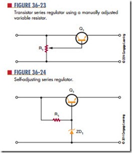
In reality, it is too difficult to vary the resistance manually to compensate for voltage and current changes. It is more efficient to replace the variable resistor with a transistor (Figure 36-23) connected so that the load’s current flows through it. By changing the current on the base of the transistor, the transistor can be biased to conduct more or less current. Additional components are required to make the circuit self- adjusting (Figure 36-24). These components allow the
transistor to compensate automatically for changes in the input voltage or load current.
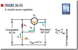
Figure 36-25 shows a simple series regulator. The input is unregulated DC voltage, and the output is a lower, regulated DC voltage. The transistor is connected as an emitter follower, meaning that there is a lack of phase inversion between the base and the emit- ter. The emitter voltage follows the base voltage. The load is connected between the emitter of the transistor and ground. The voltage at the base of the transistor is set by the zener diode. Therefore, the output voltage is equal to the zener voltage minus the 0.7-volt dropped across the base-emitter junction of the transistor.
When the input voltage increases through the transistor, the voltage out also tries to increase. The base voltage is set by the zener diode. If the emitter becomes more positive than the base, the conductance of the transistor decreases. When the transistor conducts less, it reacts the same way a large resistor would react if placed between the input and output. Most of the increase in input voltage is dropped across the transistor, and there is only a small increase in the output voltage.
There is a disadvantage with the emitter-follower regulator because the zener diode must have a large power rating. Zener diodes with large power-handling capabilities are expensive.
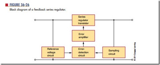
A more popular type of series regulator is the feedback regulator. A feedback regulator consists of a feedback circuit to monitor the output voltage. If the output voltage changes, a control signal is developed that controls the transistor’s conductance. Figure 36-26 shows a block diagram of the feedback regulator. An unregulated DC voltage is applied to the input of the regulator. A lower, regulated DC output voltage appears at the output terminals of the regulator.
A sampling circuit appears across the output terminals. A sampling circuit is a voltage divider that sends
a sample of the output voltage to the error-detection circuit. The voltage changes if the output voltage changes.
The error-detection circuit compares the sampled voltage with a reference voltage. In order to produce the reference voltage, a zener diode is used. The difference between the sample and reference voltages is the error voltage. An error amplifier amplifies the error voltage. The error amplifier controls the conduction of the series transistor. The transistor conducts more or less to compensate for changes in the output voltage.
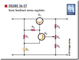
Figure 36-27 shows a feedback voltage regulator circuit. Resistors R3, R4, and R5 form the sampling circuit. Transistor Q2 acts as both the error-detection and
error-amplification circuits. Zener diode D1 and resistor R1 produce the reference voltage. Transistor Q1 is the series regulator transistor. Resistor R2 is the collector load resistor for transistor Q2 and the biasing resistor for transistor Q1.
If the output voltage tries to increase, the sample volt- age also increases. This increases the bias voltage on the base of transistor Q2. The emitter voltage of transistor Q2 is held constant by zener diode D1. This results in tran- sistor Q2 conducting more and increasing the current through resistor R2. In turn, the voltage on the collector of transistor Q2 and the base of transistor Q1 decreases. This decreases the forward bias of transistor Q1, causing it to conduct less. When transistor Q1 conducts less, less current flows. This causes a smaller voltage drop across the load and cancels the increase in voltage.
The output voltage can be adjusted accurately by varying potentiometer R4. To increase the output voltage of the regulator, the wiper of potentiometer R4 is moved in the more negative direction. This de- creases the sample voltage on the base of transistor Q2, decreasing the forward bias. This results in transistor Q2 conducting less, causing the collector voltage of transistor Q2 and the base of transistor Q1 to increase. This increases the forward bias on transistor Q1, causing it to conduct more. More current flows through the load, which increases the voltage out.
A serious disadvantage with the series regulator is that the transistor is in series with the load. A short in the load would result in a large current flowing through the transistor, which could destroy it. A circuit is needed to keep the current passing through the transistor at a safe level.
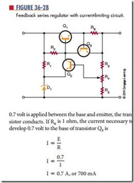
Figure 36-28 shows a circuit that limits current through the series regulator transistor. It is shown added to the feedback series voltage regulator. Transistor Q3 and resistor R6 form the current-limiting circuit. In order for transistor Q3 to conduct, the base-to-emitter junction must be forward biased by a minimum of 0.7 volt. When
When less than 700 milliamperes of current flows, transistor Q3’s base-to-emitter voltage is less than 0.7 volt, keeping it shut off. When transistor Q3 is shut off, the circuit acts as if it does not exist. When the current exceeds 700 milliamperes, the voltage dropped across resistor R6 increases above 0.7 volt. This results in transistor Q3 con- ducting through resistor R2, thus decreasing the voltage on the base of transistor Q1 and causing it to conduct less. The current cannot increase above 700 milliamperes. Changing the value of resistor R6 can vary the amount of current that can be limited. Increasing the value of resistor R6 lowers the limit on current value.
The feedback series regulator has another disadvantage: the number of components required. This problem can be overcome by the use of an integrated circuit (IC) regulator.
Modern IC regulators are low in cost and easy to use. Most IC regulators have only three terminals (in- put, output, and ground) and can be connected directly to the filtered output of a rectifier (Figure 36-29). The IC regulator provides a wide variety of output voltages of both positive and negative polarities. If a voltage is needed that is not a standard voltage, adjustable IC regulators are available.
In selecting an IC regulator, the voltage and load current requirements must be known along with the electrical characteristics of the unregulated power sup- ply. Their output voltage classifies IC regulators. Fixed voltage regulators have three terminals and provide only one output voltage. They are available in both positive and negative voltages. Dual-polarity voltage regulators can supply both a positive voltage and a negative voltage. Both fixed- and dual-polarity voltage regulators are available as adjustable voltage regulators. If using any of the IC voltage regulators, refer to the manufacturer’s specification sheet.
Questions
1. What is the purpose of a voltage regulator in a power supply?
2. What are the two basic types of voltage regulators?
3. Which type of voltage regulator is used more?
4. Draw a schematic of a simple zener diode volt- age regulator, and explain how it operates.
5. Draw a block diagram of a series feedback regulator, and explain how it operates.
