Chapter 7: Specialized Interfaces for Peripheral Devices
This chapter describes the interfaces for connecting peripheral devices, from the most essential (e.g., keyboard, monitor, mouse, and printer) and multimedia (video and audio devices) to those used for entertainment purposes (the joystick and its relatives).
7.1 Keyboard Interface
A traditional PC keyboard is a standardized input device that has a standard connector and serial communication interface with the motherboard. Currently, so-called enhanced AT or PS/2 keyboards, which have over 100 keys, are used. They have supplanted the first AT keyboards, not to mention XT keyboards. XT and AT keyboards have interfaces that are electrically identical, except that the AT’s is bidirectional, which allows commands to be received from the motherboard. However, the keyboards are incompatible in terms of the logical interface (sometimes, an AT keyboard has an XT/AT mode switch). The PS/2 keyboard differs from the AT keyboard only in its connector; an adapter may be used to connect a PS/2 keyboard to an AT connector.
All keyboards have an embedded microcontroller that registers the keys being pressed and released; moreover, the next key is registered even if several keys pressed previously have not been released. When a key is pressed, the keyboard sends a scan code, which identifies the location of the key, to its controller. When a key is released, the keyboard sends this key’s scan code that indicates the releasing. After a key has been pressed for a certain period of time, the keyboard starts autorepeating the scan code of this key. The delay between the key is pressed and the autorepeat starts is called the typematic delay; the rate at which the scan code of the pressed key is autorepeated is called the typematic rate; both can be programmed in AT keyboards. The expanded keyboard has three sets of scan codes, one of which can be active.
As the USB bus has become more widely used, keyboards using this interface have appeared; they also have a built-in hub to connect, for example, a mouse. The USB keyboard is powered from the bus. The USB keyboard needs support from BIOS of a motherboard; modern motherboards provide this function.
7.1.1 AT and PS/2 Keyboard Interfaces
Keyboards are connected using a serial synchronous bidirectional interface that consists of two mandatory signals: KB-Data and KB-Clock. Both lines are pulled by resistors to the +5 V rail on the motherboard bus. The low level of output signals is formed at the both ends of the interface by open-collector (drain) type gates; the lines’ status can be examined via the controllers’ input lines. Keyboard connectors on a PC’s back panel and their pinouts are shown in Fig. 7.1. There are two versions of the physical connector: the regular 5-contact DIN socket for the AT keyboard, and the mini-DIN socket for PS/2. The keyboard’s +5 V power supply is routed to this connector via a fuse. The mini-DIN connector may also have PS/2 mouse signals (for built-in trackballs).
Caution
Devices like external data storage devices or LAN adapters that are connected to the parallel port often use the keyboard connector power supply line. The fuse installed on the motherboard may not be able to handle the current surge generated by these devices. This will also disable the keyboard: its indicators will not even blink when the system is powered up.
The processor communicates with the keyboard through the keyboard interface controller—an 8042 microcontroller (or one that is software-compatible with it) installed on the motherboard. Information exchange is conducted mainly through port 60h, from which scan codes are received. The controller alerts the processors of the necessity to read a scan code via the IRQ1 hardware interrupt. This interrupt is generated every time a keyboard event happens (i.e., a key is pressed or released). Commands sent to this port also set the typematic delay and rate, select scan code tables, control the keyboard’s LED indicators, manage key matrix scanning, and perform diagnostic tests. The controller translates commands into code messages and sends them to the keyboard.
Fig. 7.2, a illustrates how a bidirectional interface works; signals generated by the controller are shown in gray; those generated by the keyboard are shown in black. In the initial state, both lines are held in the high-level state by the output gate circuits. The keyboard can begin sending data at any moment when the interface is idle. The keyboard places a start bit (low level) on the KB-Data line, and by issuing the first KB-Clock impulse notifies the controller that it must begin receiving data. After the KB-Clock goes high, the keyboard places data bit 0 on the KB-Data line, followed by the next KB-Clock pulse. The controller must latch the received data bit at the fall of the KB-Clock. In this way, all 8 data bits and the odd parity bit are sent. After it latches the parity bit, the keyboard controller must generate a KB-Clock impulse (Ack) acknowledging the recept of the byte. If the controller does not receive the byte, including the parity bit, within 2 msec, it stops receiving the current byte and records a time-out error.
The reverse transmission—sending a command from the controller to the keyboard—is somewhat more complex (Fig. 7.2, b). From the idle state, the controller drives the KB-Clock line low for 250 μsec, and generates a start bit by driving the KB-Data line low. This is the signal for the keyboard to start receiving commands. The keyboard must answer it with a series of 11 KB-Clock pulses. At the fall of the next clock, the controller places the next data bit, and the keyboard latches it at the rise of a clock pulse that it now generates itself. In this way, all eight data bits, the ninth (parity) bit, and the tenth (stop) bit of a command are sent. At the 11th pulse, the keyboard generates an acknowledgement bit (Ack; low level). After this, the controller requests the keyboard’s response by generating a 60-msec-long KB-Clock pulse. If the controller does not receive a response to this request within 20 msec, it generates a time-out error. An error also will be recorded if the keyboard does not generate the first clock pulse within 15 msec of the request being issued, or if the controller does not receive the data, including the stop bit, within 2 msec of the start of the clock pulse 0.
There was no 8042 controller on the PC/XT motherboard, and the keyboard interface was implemented by hardware logic; specifically, by a shift register whose parallel input was connected to the inputs of the port A of the i8255 system interface. Each time a byte was received from the keyboard, the hardware interrupt IRQ1 is generated and the interrupt handler could read the received byte out of port 60h. Bits 7 and 6 of port 61h could be used to block and reset the keyboard by software, respectively. The XT keyboard could be reset by zeroing out the KB-Clock line.
7.1.2 8042/8242 Keyboard and Mouse Controller
The programmable i8042 keyboard microcontroller is an intermediary between the keyboard, to which it is connected by the interface described above, and the central processor, to which it is connected by the parallel interface. The microcontroller continuously executes an internal microprogram monitoring signals from the keyboard and commands from the central processors. This microprogram (keyboard controller BIOS) is stored in the controller’s internal masked ROM; it is not externally accessible, and the controller may be considered as a set property device. Because the controller’s operating logic is software-implemented, it reacts to the processor’s commands and the interface’s signals relatively slowly: the response time is measured in tens of microseconds. In addition to controlling the keyboard, the software-controlled and read lines of the controller’s external ports are used to generate the Gate A20 control signals and the hardware reset signals; they are also used to read the signals from the motherboard configuration jumpers. In addition to the keyboard interface, the i8242 controller supports analogous interface for another device: the PS/2 mouse. Upon initialization (hardware reset), the controller assumes either the PS/2 or AT mode, depending on the state of the microchip’s specific pin. In the AT mode, the controller does not support mouse functions, and ignores all mouse commands. The mode is selected by the appropriate setting in BIOS Setup.
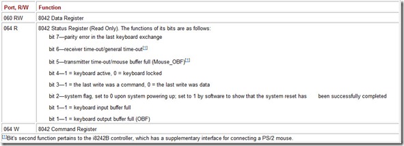
The controller communicates with the central processors via the 8-bit parallel data bus. The controller is selected by the CS# signal of the address decoder, triggered by addresses 0060h and 0064h. The controller’s internal registers are selected by the system address bus’ SA2 line. The IORD# and IOWR# signals control reading and writing; they are generated when the central processor executes instructions IN and OUT, respectively. Subsequently, the controller occupies addresses 60h (data register) and 64h (command and status register) in the CPU I/O address space. The functions of the controller’s registers are listed in Table 7.1. Data received over the interfaces from the keyboard and mouse, and data that the controller sends in response to the commands issued to it, are read out of the data register. The data register is written to in order to issue both commands and data addressed to the keyboard and mouse, as well as data addressed to the controller. Commands addressed to the controller are written into the command register. The controller’s operating mode (keyboard and mouse interface and interrupt enabling, scan code transmission, and other parameters) is set by the command byte that is sent to the controller by a special command. Before anything is written to the controller, its availability must be ascertained. Bit 1 of the status register (port 064h) indicates controller’s being ready/busy state.
Table 7.1: Table 7.1. Keyboard Controller Register Functions
The controller has two external ports, which are used to implement the serial interfaces and to control GateA20. They also are used to control the processor reset signal and to read the signals from the motherboard configuration jumpers and the keyboard lock key. These ports are not mapped to the PC’s I/O space, but are accessed using the controller commands. In addition to these two ports, the controller has two special inputs: T0 and T1. The controller’s program can read these inputs and use them as the internal interrupt source (they are not CPU interrupts). Each of the bidirectional KB-Data, KB-Clock, MS-Data, and MS-Clock lines is implemented by an output port bit and by an input bit. In the PS/2 mode, inputs T0 and T1 are used to read the KB-Clock and MS-Clock lines; in the AT mode, the T1 input is used for the KB-Data line.
The P1 input port is accessed by the COh command; in the PS/2 mode, its bits have the following functions:
-
Bit 7—KeyLock. 0 = the keyboard is locked.
-
Bit 6—video mode setting jumper. 0 = color; 1 = mono.
-
Bit 5—system jumper. 0 = closed.
-
Bit 4—RAM size jumper. 0 = 256 KB; 1 = 512 KB and over.
-
Bits 3 and 2—not used.
-
Bit 1—MS-Data line.
-
Bit 0—KB-Data line.
Modern PCs use only bits 0, 1, and 7; in the AT mode, bits 0 and 1 are not used.
The P2 output port can be read from and written to by the D1h and DOh commands, respectively. The functions of its bits are as follows:
-
Bit 7—KB-Data line.
-
Bit 6—KB-Clock line.
-
Bit 5—mouse interrupt request (IRQ12); not used in the AT mode.
-
Bit 4—keyboard interrupt request (IRQ1).
-
Bit 3—MS-Clock line; not used in the AT mode.
-
Bit 2—MS-Data line; not used in the AT mode.
-
Bit 1—the A20 address line gate (Gate A20, see Section 12.3). 0 = A20 is zeroed out; 1 = A20 is controlled by the processor.
-
Bit 0—alternative CPU reset (without system reboot).
Having received a byte from the keyboard, the controller internally converts the scan code (if it is not forbidden by a control byte) and sets the status register bit 1 (OBF) to 1, which triggers generation of the IRQ1 interrupt request (if is not forbidden by a control byte). In response, the host must read the data (converted scan codes, prefixes, etc.) from the data register (60h). Conversion serves to make the scan codes sent to port 60h by the XT and AT keyboards software-compatible. Bytes received from the mouse are not converted by the controller; it only sets the register status bit Mouse_OBF to 1 and triggers an interrupt request IRQ 12 (if it is not forbidden by a command byte). At this signal, the host must read the mouse data from the same port 60h. The same thing happens when a byte is written into the keyboard or mouse output buffers by software (codes D2h and D3h, respectively) with the corresponding status bits set and interrupt requests IRQ1 or IRQ12 generated.
Having received a command, in response to which the controller must return data, it sets the status register bit OBF=1, which triggers the interrupt request IRQ1 (if it is not forbidden by the command byte). Then, the data must be read out of the data register (at address 60h). If the command returns several data bytes, interrupts are generated for each byte.
Communication with the controller is carried out by issuing commands to it (i.e., by writing into the command register at address 064h). Before a command is sent, it is necessary to ascertain that the controller is ready to receive it: Port 64h bit 1 must be logical zero. Keyboard controllers have different versions of the built-in software; therefore, changing one controller for another with a different software version (KBC BIOS) may cause problems: The motherboard BIOS microchip must know the keyboard controller’s characteristics.
7.1.3 System Support and Software Interface
Keyboard events and functions—pressing and releasing keys, providing services to input the symbols, controlling its parameters (typematic delay and rate) and indicators—are supported at the BIOS level. Codes received from the keyboard by the controller are read and handled by the hardware interrupt IRQ1 handler (vector 09h). The result is placed into the keyboard buffer, from where it can be extracted considerably later by the software interrupt Int 16h for further processing. The codes of the “system” key combination <Ctrl>+<Alt>+<Del>, the <Print Screen> (<Sys Rq>) key and some other keys are not placed into the keyboard buffer, but evoke special procedures. An application program that needs to use the keyboard in a nonstandard way (as a music keyboard, for example) will have to handle the IRQ1 hardware interrupt by itself by intercepting and redirecting the hardware interrupt Int 09h. This interrupt needs to be intercepted to call some TSR program function using a hotkey combination.
POST initializes the keyboard and its controller and launches a diagnostic test. During this test, all of the keyboard’s LED indicators flash momentarily, after which only the NumLock LED may remain on (depending on the BIOS settings). If there is a keyboard error, a message containing a possible scan code for the stuck key will be displayed on the monitor, and the user is usually prompted to press the F1 key to continue. The same thing will happen if POST does not detect the keyboard (because of an unplugged connector or a burnt-out fuse, for example), but in this case pressing the F1 key will not suffice. Connecting an XT keyboard to an AT computer will also produce a diagnostic error message; the reverse connection is not viable either. If for some reason it is desirable to continue POST even with a keyboard error, the keyboard testing may be disabled in BIOS setup.
The following RAM cells from the BIOS Data Area are used for the keyboard services:
-
0:0417, 0:0418—keyboard status flags
-
0:0419—the Alt key accumulator, 1 byte long
-
0:041A—Buffer Head pointer, 2 bytes long (modified on pushing a character into the buffer)
-
0:041 C—Buffer Tail pointer, 2 bytes long (modified on popping a character out of the buffer)
-
0:041E-0:042D—keyboard buffer, 16 words long
7.2 Mouse Interface
A mouse is a device for inputting coordinates and issuing commands. A mouse interface can be used in any physical implementation of the device (mouse, trackball, etc.). In terms of the computer interface, three principal types of mouse are distinguished: bus mouse, serial mouse, and PS/2 mouse. Mice with a USB interface have come out too, but they have not yet received wide acceptance; nor has the USB keyboard, to the hub of which a USB mouse can be conveniently connected.
Serial and PS/2 mouse interfaces are not compatible. Even though they are both serial, there are significant differences in their signal levels, clocking methods, frequencies, and formats of sending signals.
-
The PS/2 interface uses unipolar TTL-level signals; the mouse’s power supply is unipolar +5 V with respect to the GND rail. The RS-232 interface used by serial mice employs a bipolar signal (see Section 2.1) with thresholds of +3 V and −3 V and requires a bipolar (with respect to the GND rail) power supply.
-
The PS/2 interface uses two separate signal lines; one to send data and the other for clock signals. The serial mouse interface transmits data asynchronously only over one line.
Even without taking into consideration the frequency and format of the signals, it becomes obvious that direct compatibility between these interfaces is impossible. Nevertheless, passive (!) adapters intended to select the method to connect the mouse are produced and sold. These adapters are intended only for universal mice whose built-in controller can recognize the interface, to which it has been connected by the power supply voltage, and set the appropriate output interface. Universal mice are not that widely used, so quite often complaints can be heard about unsuccessful attempts to use these adapters with a regular serial mouse or PS/2 mouse.
Additional confusion is created by Macintosh mice that have a connector that outwardly resembles the PS/2 connector. However, upon closer examination and after an unsuccessful attempt to plug it into a PC, it becomes clear that, these are different connectors; moreover, the interface is entirely different.
7.2.1 Serial Mice: MS Mouse and PC Mouse
Serial mouse has a serial interface connected to the PC through the 9- or 25-contact COM port connector (Table 7.2). This mouse has a built-in microcontroller that processes signals from the coordinate sensors and the buttons. Each event—mouse move or a button press or release—are sent in binary code over the RS-232 interface. Data are sent asynchronously; the bipolar power supply required by the RS-232 protocol is supplied by the interface control lines. A shortcoming of the serial mouse is that it takes a COM port and monopolizes its regular interrupt line (IRQ4 for COM1 and IRQ3 for COM2). Of course, the fact that in order to service the mouse, the COM1 port needs precisely the IRQ4 interrupt is a shortcoming not of the mouse itself, but of its driver, but for a user who is not into mouse drivers, only the fact of the shortcoming itself matters. The two main mouse types—Microsoft Mouse (MS Mouse) and PC Mouse—require different drivers; many mice have MS/PC switches. These two types of mice use the same 1,200 bps transfer rate, one stop bit, and no parity, but the formats of their signals are different:
-
MS Mouse uses 7. data bits and a 3-byte packet (in the “classic” version). Movements to the right along the X-coordinate and down along the Y-coordinate are considered positive. For 3-button mice, another byte is added to the packet that is sent only when the status of the third button changes. In 3-D mice, this byte performs a different function.
-
PC Mouse uses 8 data bits and a 5-byte packet. Movements to the right along the X-coordinate and up along the Y-coordinate are considered positive.
From considering these formats, it is clear why the mouse cursor moves about the screen chaotically when a matching driver for the given mouse has not been loaded. This incompatibility may manifest itself in even more unpleasant way: When loading (or being installed), Windows 95 does not recognize a mouse operating in the PC Mouse mode (it does not “like” the identifier this mouse presents when initialized). When the OS has loaded, switching mouse modes only leads to the cursor jumping unpredictably around the screen and the buttons not working properly.
Table 7.2: Table 7.2. Serial Mouse Connectors
On the system level, the serial mouse is supported only on the operating system level (services are called via Int 33h); mouse drivers are either installable or built into the operating system’s driver library. BIOS does not support a mouse even if it uses it to navigate in the BIOS Setup. To stress one more time: A mouse requires a hardware interrupt line to operate—IRQ4 or IRQ3 for serial mice installed to ports COM1 or COM2, respectively.
7.2.2 PS/2 Mouse
The PS/2 mouse was introduced with the PS/2 computers. Its interface and the 6-pin mini-DIN connector is the same as the keyboard connector (Fig. 7.1), and as a rule is serviced by the same 8242 keyboard controller (see Section 7.1.2). Many modern motherboards are equipped with PS/2 mouse adapters and connectors (Fig. 7.3). A PS/2 mouse controller may also be implemented on an ISA expansion card. In this case, it will occupy I/O address space addresses. Communication with a PS/2 mouse is bidirectional: The processor can send special commands to the 8242 controller; however, unlike in the keyboard interface, before a “mouse” byte is written to port 60h (a command and its parameters), code D4h must be written to port 64h.
The PS/2 mouse can operate in one of two modes. In the stream mode, the mouse sends data upon any change in its state; in the remote mode, it sends data only when requested by the processor. There also is the diagnostic wrap mode, in which the mouse returns data sent to it by the controller. When the controller receives a packet from the mouse, it sets the Mouse_OBF flag and generates the IRQ2 interrupt request, if it is not disabled by the 8242 command byte.
Setting PS/2 mouse parameters by sending to it the above-described commands is supported at the BIOS level. The mouse driver itself (IRQ12 interrupt handler at vector 74h) that services its data transmissions is a part of the operating system to be loaded separately. Mouse support is enabled via functions C200h-C209h of the BIOS Int 15h.
7.2.3 Bus Mouse
The bus mouse was one of the first versions of the mouse. The mouse itself contains only sensors and buttons. The controller to process signals from the mouse is located on a separate adapter, usually of ISA type. The mouse has nine-wire cable with a special connector (Fig. 7.4) that at first glance resembles the PS/2 Mouse connector. The major shortcoming of this system is that the adapter needs to be allocated system resources such as a bus slot, I/O space addresses, and an interrupt request line. Some vendors used to offer Multiport ISA cards (COM, LPT, and GAME ports) with a bus mouse adapter. Because Microsoft was one of the first to offer this type of mouse and the mouse had its logo, the MS Mouse is sometimes associated with the bus mouse. However, the MS Mouse can operate under any of the three interfaces.
7.3 Printer and Plotter Interfaces
Modern high-resolution graphics (including text in graphics mode) printers demand a high-rate external data-transfer interface. Most printers use either the traditions parallel Centronics or more efficient IEEE 1284 interface. The latter allows transmission speeds of 0.15 MBps-2 MBps, depending on the computer’s efficiency and the selected transfer mode. Plotters use the same interfaces.
Various modifications of the LPT port are used to connect a parallel interface printer, from the traditional SPP to the today’s standard efficient IEEE 1284 (see Section 1.3).
Originally, all parallel interface printers necessarily supported the Centronics interface, and the more advanced could even work in the ECP mode supporting the IEEE 1284 negotiation sequence. Their installers tried to install drivers that supported the advanced modes if the operating system and the LPT port capabilities allowed this. The situation has changed, and now there are printers that do not support the Centronics interface. During installation, they request to be connected using the bidirectional IEEE 1284 interface (usually, in the ECP mode) and refuse to work with the LPT port in the SPP mode. These printers require special drivers to be used with MS-DOS operating system.
Some printers use serial interfaces, such as RS-232C, RS-422, or the current loop. However, the theoretical transfer-rate limit of these interfaces is about 115 Kbps, and the actual transfer rate barely reaches 9,600 bps. These printers can be connected to a COM port directly, or by using a signal-level converting adapter.
Lately, the USB is being used more and more often to connect printers, but this switch over is not exactly trouble-free, since not all operating systems support USB. Old applications (the possibility of switching over to new ones does not always exist) that work with the printer using the BIOS Int 17h functions or directly with the LPT port registers (to prompt inserting a blank sheet of paper, for example) cannot work with a USB printer, even if the operating system fully supports USB. In terms of the data transfer rate, the USB 1.0, at 12 Mbps, is far from reaching speeds of 1.5 MB/sec (12:8) because of the bus overhead alone. The USB 2.0 offers peak speeds of up to 50 KBps (the bus speed is 480 Mbps), which for a printer is more than enough for the time being. However, in this case the printer and the computer have to support USB 2.0 and there must not be old (USB 1.0) hubs between them.
Printer may use the SCSI interface, but this is not common. They also may be connected not to a computer but to a local network using the Ethernet protocol (10 or 100 Mbps). It is convenient to connect shared printers in this way, and with a properly set-up network it serves users without problems. The FireWire bus has had some very limited use for connecting printers so far.
7.3.1 Centronics and IEEE 1284 Parallel Interfaces
The Centronics parallel interface is oriented at transmitting a data stream to the printer and receiving printer status data. This interface is supported by all LPT ports. The term “Centronics” is used to describe both the signal suite and interaction protocol and the 36-contact printer connector. The functions of this interface’s signals are listed in Table 7.3. Printer exchange timing diagrams are shown in Fig. 7.5.
Table 7.3: Table 7.3. Centronics Interface Signals
Data transmission starts with checking the status of the Busy line to establish whether the printer is ready. The data strobe may be fractions of a microsecond long, and the port finishes forming it regardless of the Busy signal state. During the strobe, the data must be valid. The Ack# signal confirms receiving a byte. It is generated an indeterminate interval after the printer receives the strobe. (During this time, the printer may perform some lengthy operation, such as paper feed.) By sending an Ack# pulse, the printer requests the next byte to be sent; this pulse is used to generate a printer port interrupt request. If interrupts are not used, the Ack# signal is ignored, and the data exchange is controlled by the Strobe# and Busy signals. The printer may inform the port of its status over the Select, Error#, and PaperEnd lines, which indicate whether the printer is turned on, in working order and not out of paper, respectively. The printer may be reset by pulsing the Init# line; this will also clear its data buffer. The automatic line feed mode is not normally used, and the AutoLF# is set high. The Select In# signal logically disconnects printer from the interface.
The Centronics protocol can be implemented over the parallel port purely by software using the SPP mode; speeds of up to 150 KBps at full processor load can be reached. Thanks to the advanced port modes, the protocol can be hardware-implemented (Fast Centronics), reaching speeds of up to 2 MBps at a lower processor load.
Most modern parallel interface printers also support the IEEE 1284 standard, in which the optimal transfer mode is the ECP. (See Section 1.3.4.)
A Centronics cable, suitable for any parallel interface mode, is used to connect the printer. The simplest version of the cable—18-wire with non-twisted pairs—can be used for the SPP mode. If the cable is over 2 m long, it is desirable that at least the Strobe# and Busy lines be intertwisted with individual common wires. For the highspeed modes, this cable may not be adequate, and may cause intermittent errors occurring only when certain code sequences are sent. There are Centronics cables that do not have contact 17 on the PC connector connected to contact 36 on the printer connector. Attempting to connect the printer operating under the 1284 standard using this cable will produce a system message to the effect that a “bidirectional cable” needs to be used. The printer cannot inform the system that it supports the expanded modes as the printer driver expects. Another manifestation of the missing contact 17-36 link is that the printer hangs after finishing a Windows printing job. This missing-link problem can be solved by soldering an extra wire between these two contacts, or simply replacing the cable with one where these contacts are connected.
The electrical properties of ribbon cables, with their alternating signal and common wires, are not too bad. But these cables are not practical for external use: Just one insulation layer makes them rather vulnerable to physical damage. Besides, they do not fit well with considerations of interior design: Round cables look better.
The ideal solution is shielded cables with a twisted wire pair for each signal, as this requires the IEEE 1248 standard. These cables are guaranteed to deliver speeds of up to 2 MBps at distances of up to 10 meters.
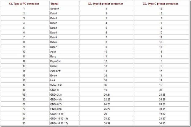
Table 7.4 shows the wiring of a printer connection cable to the XI Type A (DB25-P) connector on the computer side and to the X2 Type B (Centronics-26) or Type C (miniature) connectors on the printer side. Whether the common GND wires are used depends on the quality of the cable. In the simplest (18-wire) cable, all ground signals are brought into one wire. Quality cables require a separate return wire for each signal line; however, Type A and B connectors do not have enough contacts to comply with this requirement (Table 7.4 shows in parentheses Type A connector contacts that have return wires). The Type C connector has a return (GND) wire for each signal wire; contacts 19-36 are the corresponding ground contacts for the signal contacts 1-17.
Table 7.4: Printer Connection Cable
7.4 Graphics Adapter Interfaces
Special interfaces are used for connecting a monitor to the computer’s graphics adapter. Information about the instantaneous intensities of the primary colors (RGB) and the line and frame synchronization signals are transmitted over these interfaces. The transmission method has already made its first spiral of development, from the digital interface of the first adapters (MDA, CGA, EGA) through the analog VGA interface, and back to the digital interfaces (DVI, P&D, DFP). Most of the monitor interfaces have been standardized by VESA (http://www.vesa.org).
Video interfaces are used to output information to regular television sets and computer monitors, as well as to input data to the computer. Digital video data can be transferred over the FireWire and USB 2.0 buses.
Many graphic adapters have an internal VFC or VAFC connector. This is a parallel bus for exchanging pixel information with supplementary video cards.
A graphic adapter is connected to the processor and main memory via one of the expansion buses: AGP, PCI, or ISA, the interfaces of which are described in Chapter 6.
7.4.1 RGB TTL Discrete Interface
The discrete TTL level interface—RGB TTL—was used in monitors connected via MDA, HGC (Hercules), CGA, and EGA graphic adapters. This interface requires a DB-9 connector (female on the adapter); its signals are listed in Table 7.5. Monochrome displays use only two signals: Video (beam on/on) and Intens (beam intensity). Color Display class monitors for CGA adapters use one signal to control each color beam and one common beam intensity control signal; this allowed 16 colors to be specified. The Enhanced Color Display (ECD) for the EGA adapter requires two control signals for each primary color: One for the higher bit and the other for the lower bit of the primary colors—RED, GREEN, BLUE and Red, Green, Blue. In this way, 64 colors can be specified.
Table 7.5: Discrete Monitor Interface (RGB TTL)
The H. Sync and V. Sync signals control the monitor’s line and frame sweep, respectively. High resolution (720 × 350 pixels) monochrome MDA and HGC adapters employ a high frequency sweep. The CGA adapter works at low frequencies; its sweep frequencies are close to those of television. EGA adapters and monitors can work with any of these frequencies. The V. Sync is used to facilitate switching the monitor’s sweep generator modes: The polarity of the pulses determines the current mode’s sweep frequency range.
7.4.2 Analog RGB Interfaces
The RGB Analog interface employs an analog method to transmit primary-color signals, which allows a nominally indefinite number of hues to be transmitted. In modern adapters, primary-color signals are generated by 8-bit DACs, allowing 16.7 million hues (True Color) to be represented. In order to reduce interference, these signals are sent over twisted wire pairs, each of which has its own Return wire. Inside the monitor, each signal pair is loaded by a resistor in order to match the cable impedance. Black is represented by zero potential on all color lines, full brightness is represented by +0.7 V (not all graphic adapters support full signal amplitude). Control, status, and synchronization signals are sent by TTL levels. RGB interface timing diagrams (also applicable to the RGB TTL) are shown in Fig. 7.9. The R, G, and B signals are shown symbolically; depicted are the time intervals during which the signals illuminate screen dots (the visible part of the image is in the area where the line scan and frame refresh signals overlap; the rest of the time, the beam is turned off). Only the main timing parameters of the signals are shown in the illustration. The VESA DMT (Discrete Monitor Timing, 1994-1998) standard specifies a discrete series of parameter sets for various display resolution modes. A later standard, VESA GTF (Generalized Timing Formula), provides formulas for determining all synchronization parameters. The source data for the calculations are as follows:
-
Display resolution in pixels (800 × 600, for example)
-
Overscan border requirements
-
Non-interlaced or interlaced line sweep
-
One of the frequencies: frame, line, or pixels
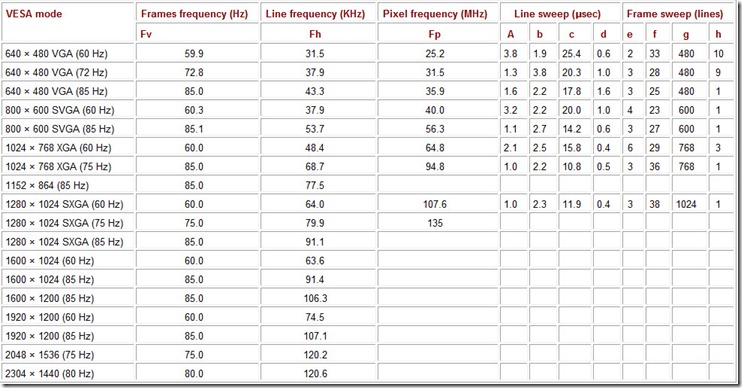
Because there are many standards, the same set of parameters used by different graphic adapters and their drivers will have slightly differing signal timing parameters. These variations have to be compensated by adjusting the monitor (image size and vertical and horizontal positions). Table 7.6 shows some examples of line sweep synchronization parameters. For line sweep, synchronization parameters are given in μsec, and for the frame refresh they are given in the number of lines during this time.
Table 7.6: Synchronization Parameters
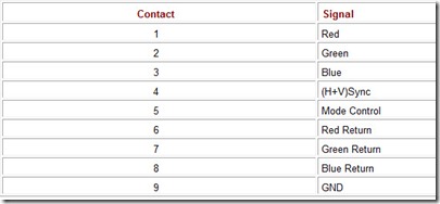
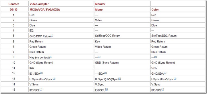
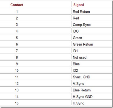
An analog interface was used for the first time by IBM in its PGA adapter, which employs a 9-pin DB-9S connector (Table 7.7). Later, starting with the VGA adapters, a 15-contact compact connector of the same size was employed (Table 7.8). For the most part, the signal functions of these interfaces are identical; there even are 15- to 9-contact connectors adapter cables (Table 7.9). Line and frame synchronizations in PGA adapters are done by one composite (H+V) Sync signal. This mode is called Composite Sync and is supported by many modern monitors.
Table 7.7: PGA Monitor Analog Interface (DB-9S Connector)
Table 7.8: VGA Monitor Analog Interface (RGB Analog)
[1]DDC signals Return, SDA, and SCL can be used only with DDC support. In this case, contact 9 can be used to supply power to the DDC logic (+5 V).
[2]The (H+V)Sync signal is used with the Composite Sync.
Table 7.9: Nine-to-15 Monitor Interface Connector Adapter
Even though the 15-contact connectors have a physical key—the D-case—quite often users manage to insert them in reverse. When this happens, one of the middle row contacts bends and eventually breaks off (pins on 15-pin connectors are thinner and more fragile then on 9-pin ones). Naturally, a monitor connected in this way will not work.
Macintosh computers, which are compatible with the VGA standard, have a DB-15P connector, the same as the PC’s game port connector. The functions of its contacts are given in Table 7.10.
Table 7.10: Macintosh VGA Connector
In addition to the image, the information necessary to automate the computer and monitor parameter matching is sent over the interface. The computer’s “interests” are represented by the display adapter to which the monitor is connected. The adapter performs monitor identification that is necessary to provide Plug and Play support and to control the monitor’s power consumption.
To perform the simplest identification, four logical signals ID0-ID3 were added to the interface. Using these signals, the adapter could identify the IBM monitor connected. On the monitor side, these lines were either connected to the ground or left unconnected. However, in this identification system, only the ID1 signal was employed, used to indicate the fact that a monochrome monitor was connected. The adapter can identify a monochrome adapter in another way, namely, by the absence of load on the Red and Blue lines.
The parallel monitor identification method was replaced with the serial method using the VESA DDC (Display Data Channel) digital interface channel. This channel is implemented using either the I2C (DDC2B) or ACCESS.Bus (DDC2AB) interfaces, which require only two TTL signals: SCL and SDA. The DDC1 interface is unidirectional: The monitor sends to the adapter a block of its parameters over the SDA line (contact 12); this transmission is synchronized by the V.Sync signal (contact 14). While it is receiving this parameter block, the adapter may raise the frequency up to 25 KHz (the vertical-scanning generator cannot be synchronized at such high frequency). The DDC2 interface is bidirectional, using the dedicated SCL signal (contact 15). The DDC2AB interface differs in that it allows peripheral devices that do not require high transfer exchange rates be connected to the computer over the ACCESS.Bus serial bus (see Section 11.1.2.)
The Extended Display Modification (EDID) parameter block has the same structure for any type of DDC implementation (Table 7.11).
To control the monitor’s power consumption, the V.Sync and H.Sync frame and line synchronization signals are used in accordance with the VESA DPMS (Display Power Management Signaling) standard (Table 7.12.)
Table 7.12: Controlling Monitor Power Consumption (VESA DPMS)
Connectors used in modern adapters and SVGA monitors are not designed to transmit high-frequency signals. Their upper limit is approximately 150 MHz, which is not enough for high resolution and high refresh rate. Therefore, large, high-resolution, high synchronization frequency professional monitors and their corresponding adapters are equipped with BNC connectors for connecting via a coaxial cable. Monitors equipped with coaxial cable connectors can be connected to graphic adapters equipped with DB-15 connectors using special matching cable adapters. These cables can have three to five 75-ohm coaxial BNC connectors:
-
Three connectors—primary-color signals; composite sync is sent over the green color channel.
-
Four connectors—composite sync is sent over a separate cable.
-
Five connectors—vertical and horizontal are transmitted over separate cables.
Using coaxial cables, the monitor may be located up to 10-15 meters from the computer and retain the quality of the image.
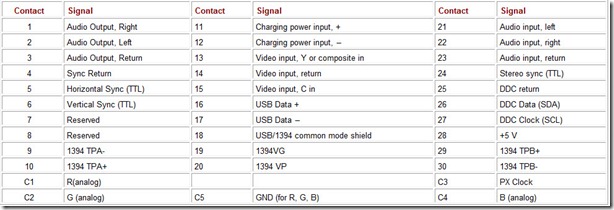
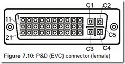
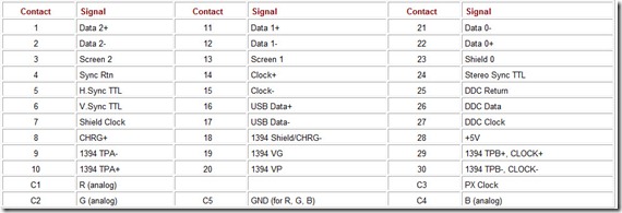
To expand the frequency range (and taking into account the tendency to use serial buses like USB and FireWire), in 1995 VESA put forward a new type of connector—Enhanced Video Connector (EVC)—to connect peripheral devices to the system block. In 1998, a new edition of this standard was accepted introducing minor modifications related to reserved contacts and charging device power lines. The connector also was renamed as Plug&Display-Analog (P&D-A). In addition to the regular analog RGB interface and the DDC2 channel, the P&D-A (EVC) connector has contacts for video input, incoming and outgoing stereo audio signals, USB and FireWire buses, as well as direct current power supply lines to charge the batteries in a portable PC. The connector is divided into two parts: a high-frequency section for connecting four coaxial cables, and a low-frequency 30-contact section (Fig. 7.10 and Table 7.13). Even though the high-frequency section contacts are not of the coaxial kind, they allow signals with frequencies of up to 2 GHz to be sent. Cables’ shields are connected to the cross-like contact divider. When using 75-ohm coaxial cables, the level of signal bounce and crosstalk at 500 MHz is guaranteed to be no higher than 2%. The high-frequency section—contacts C1-C4 and C5 (shield)—is used to transmit the RGB color signals and the PX Clock pixel synchronization signal. The pixel synchronization signal is used by digital matrix displays; using it makes it possible to reduce the video information transmission error rate. This signal’s frequency equals either the pixel scan frequency or half of it. (High frequency requires double synchronization, at the rising and falling edges, which evens out the bandwidth requirements for the color data lines and the pixel synchronization lines.)
Table 7.13: P&D-A (EVC) Connector
The connector is divided into two compact areas for each signal group, although the USB and 1394 buses use a common shield contact. The functions of the video input contacts (S-Video or composite, PAL or NTSC) can be programmed over the DDC2 channel.
The standard defines three implementation levels: basic, multimedia, and full. The basic level only contains video signals and the DDC; the multimedia level must have audio signals. When all connector capabilities are used, the monitor turns into a switchboard connected by one cable to the computer, and the rest of the peripheral devices (including the keyboard, mouse, printer, etc.) are connected to the monitor. The connector may be used to connect a portable PC to the docking station. The EVC collects signals from various subsystems: graphic, video, audio, serial bus, and power supply. This common connector is mounted on the system block case; various expansion cards can be connected to it by internal cables with matching connectors. This connector should not be confused with the similarly looking and named P&D-A/D connector, which is described in the following section. EVC connectors are not very often encountered in PCs, and not only because of their high price. It is inconvenient to install an EVC connector on a graphic adapter card, as it sprouts superfluous interface cables; integrated motherboards seldom have high-quality adapters requiring an EVC connector.
7.4.4 Digital Interfaces P&D, DVI, and DFP
The widespread migration to digital technologies has not passed monitors by. The traditional analog video signal transmission channel has become the video system’s bottleneck. On its way from the DAC to the monitor’s input video amplifiers, the signal has to pass through a pair of connectors and a cable. A mismatch of the components’ characteristics, causing signal “jitter” and irregular frequency characteristics, distorts the shape of the color signals, which becomes especially noticeable when operating in the high resolution and high refresh frequency rate modes. The image quality can be improved by placing the DAC device right into the monitor, on the video amplifier board, and feeding the digital signals into them. Flat-screen displays (built using thin-film transistor (TFT) technology) are implemented on the basis of digital technology, and have to convert incoming analog signals back into digital. All these reasons have led to the development of a digital interface for transmitting information to the monitor. This interface is required to provide an enormous bandwidth: for example, to operate at a pixel frequency of 150 MHz and 24-bit pixel coding (True Color) a bandwidth of 3.6 Gbps (450 MBps) is required.
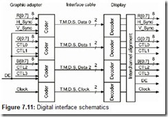
To connect flat-screen displays, the special PaneLink interface was developed; in 1996, its specification—FPDI-2—was approved by VESA. The interface’s schematic is shown in Fig. 7.11. The interface has three data transmission channels (Data [0:2]) and a clocking channel Clock. Signals are transmitted using the Transition Minimized Differential Signaling (T.M.D.S.) protocol. Each data channel consists of a coder, which is located on the video adapter, and a decoder, which is located in the monitor. The 8-bit primary color intensity code of the current pixel is input into each coder. In addition to these data, the line and frame synchronization signals are input into the channel 0 coder and supplementary control signals CTL[0:3], a pair foreach channel, are input into the channel 1 and 2 coders. The coders convert data into a serial code. In order to minimize switching, the 8 input bits are coded into a 10-bit symbol that is sent over the channel serially. Depending on the status of the input data-enabling signal, the decoders transmit either color channel data or synchronizing signals and control bits. On the receiving side, signals are decoded and restored to the same state in which they arrived at the coders’ inputs. Pixel frequency may reach 165 MHz; the interface provides maximum resolution of 1280 × 1024 (24 bits per pixel).
Physical lines are implemented using shielded twister pairs. The transmitters are differential switched 12-milliampere current sources; inputs of the differential receivers are pulled up to a +3.3 V power supply by load resistors; the signal amplitude is 500 millivolts. The coding method can be used to transmit signals over a fiber channel (the signal does not have a zero frequency component), but so far, the specification defines only the electrical interface.
The protocol described above is used in the P&D, DVI, and DFP interfaces. The most commonly used protocols are the DVI, as the most powerful and universal, and the DFP, as the cheapest specialized. Many graphics adapters with two outputs are equipped with connectors for these interfaces. The rarely encountered P&D interface may be considered a combination of cut-down versions of the EVC and DVI protocols. Because the signals (T.M.D.S.) are standardized, if the monitor and the video card are equipped with different connectors, they can be matched by passive adapters.
The VP&D (VESA Plug-and-Display, 1997), or P&D, interface uses the same connector as the EVC protocol (Fig. 7.10). It does not have analog audio signal circuits and video input; these contacts are given over to the digital signal transmission channels.
There are two versions of the interface: combined and purely digital. The combined P&D-A/D connector also has contacts for analog signals (RGB and synchronization), which makes it possible to connect digital as well as the traditional analog monitors. The strictly digital. P&D version does not have analog signal contacts; an analog monitor (with an EVC or P&D-A connector) will not work with it (the connector’s construction will not even allow it to be connected). Similarly, a purely digital monitor with a P&D input connector cannot be connected to an R&D-A (EVC) output connector.
Table 7.14: P&D-A/D Connector
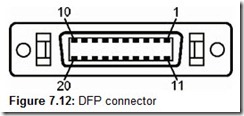
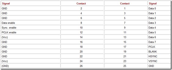
The Digital Flat Panel (DFP, 1999, http://www.dfp-group.org) interface uses an inexpensive MDR type (mini-D ribbon) connector with ribbon contacts (Fig. 7.12). On this connector, there are only three pairs of signals for digital data channels, a pair of signals for the digital synchronization channel, +5 V power supply lines, the DDC2 channel (Table 7.15), and the Hot Plug Detect signal (HPD). The pixel frequency may reach 85 MHz (flat monitors do not need a very high sweep frequency). The interface supports resolutions up to 1280 × 1024 (24 bits per pixel).
Table 7.15: DFP Connector
The Digital Visual Interface (DVI) was developed by the Digital Display Working Group (DDWG, http://www.ddwg.org) in 1999. It is aimed at connecting any type of displays (CRT and LCD) to the computer, and there are two versions of the interface and its connectors: a purely digital and a combination of digital with the traditional analog signals. In the latter case, a regular analog VGA interface monitor can be connected to a DVI connector with the help of a passive adapter.
A minimal capability digital interface version consists of a synchronization channel and three data channels (Data 0-2). This version is almost the same as the analog: Only the location of the DAC is changed and data are transferred digitally. However, the interface makes provisions for increasing the bandwidth by using time more efficiently. In traditional CRT monitors, the line and frame beam back travel takes a rather considerable amount of time, during which the screen pixels are naturally not updated and the interface is, therefore, idle. Matrix displays do not require these pauses; therefore, the same pixel information volume can be sent over a longer time, practically over the entire frame period. Consequently, either the pixel transmission frequency can be lowered (without changing the resolution or the sweep frequency) or the resolution and/or sweep frequency raised at the same pixel transmission frequency (its upper limit). The DVI specification implies extending data transmission for the duration of the entire frame in digital displays by using conventional CRTs and also by employing internal buffering.
In a monitor equipped with screen buffers, other improvements are possible: Instead of refreshing the screen continuously, which is what traditional video adapters are occupied in doing, it is possible to send data only when the image changes. This is, however, only a possible development. The full version of the DVI interface has three additional digital channels (Data 3-5); the information load must be distributed evenly between the channel pairs. Thus, even pixels will be sent over channels 0 (R), 1 (G), and 2 (B); accordingly, the odd pixels will be sent over channels 3, 4, and 5. The interface allows the transmission of pixels at frequencies up to 330 MHz (165 × 2). Provisions have been made for alternative use of the channels: When eight bits may not seem enough to encode the primary colors, channels 3, 4, and 5 may supplement (as lower bits) data of channels 0, 1, and 2 (upper bits).
In addition to the T.M.D.S. signals, the DVI interface contains VESA DDC2 interface signals, DDC Data, and DDC Clock, as well as the +5 V power supply lines, which allows the configuration information to be exchanged even when the monitor is turned off. The configuration information allows the system to determine the monitor’s capabilities and to configure the available data channels properly, matching the capabilities of the video card and the display. There also is a HPD signal, which the system uses to keep track of the monitor’s connections and disconnections. The connectors are physically constructed in such a way as to support hot connection by ensuring the proper sequence of different contact groups’ connection or disconnection. Therefore, DVI displays provide all the functions necessary to implement Plug and Play standards. The DVI interface and displays must provide standard (VESA) graphic modes, starting from 640 × 480/60 Hz (22.175 MHz pixel frequency). Its upper limit is 2048 × 1536 pixels (330 MHz pixel frequency). The interface supports Display Power Management Signaling (DPMS).
Fig. 7.13 shows DVI connectors; their pinouts are given in Table 7.16.
Table 7.16: DVI Connector
7.4.5 Internal Digital Interfaces
In order to expand a digital adapter’s capabilities, mainly in the area of video image processing, many graphics adapters are equipped with an internal interface to transmit pixel information synchronously with screen refreshing. This interface is employed to link graphic adapters with overlay cards (videoblasters) and MPEG decoders. The graphics adapter connector is linked to the same connector on the video card by a ribbon cable.
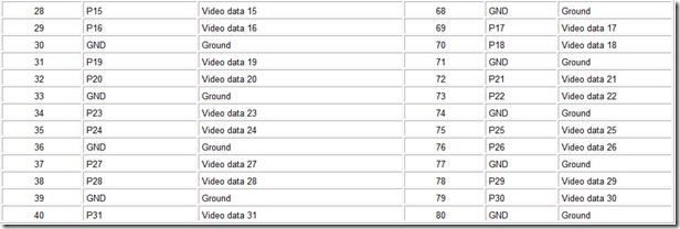
VGA adapters used to have a 26-contact edge VGA Auxiliary Video Connector with contact pads spaced 0.1 inch apart. Later, the VESA Feature Connector (VFC) (Table 7.17) was standardized; its signal suite is practically the same, but a two-row pin connector is used. This VGA and SVGA graphic adapter connector makes it possible to receive the flow of data bytes of the scanned pixels with the adapter operating in modes of up to 640 × 480 × 8 bits.; Usually, the interface outputs data and is clocked by the graphics adapter clock. However, by setting the Data Enable signal low, the video card can force the graphics adapter to receive pixels; the Sync Enable signal switches the graphic adapter into receiving the line and frame synchronization signals; the PCLK Enable signal switches the graphic adapter into operating from the external pixel synchronization signal.
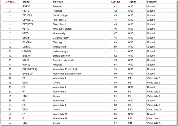
The VESA Advanced Feature Connector (VAFC) (Table 7.18) is designed to be used in up to 1024 × 768 High Color (16 bit) and True Color (24 or 32 bits) operating modes. It has two rows of contacts spaced 0.05 inch apart, with 0.1 inch between the rows. It is 16/32 bits wide, and at the maximum dot frequency of 37.5 MHz provides data flow speed of 150 MBps. The 16-bit VAFC version uses the first 56 contacts; the 32-bit version uses all 80 contacts. The maximum ribbon cable length is 7 inches. In this interface, the GRDY and VRDY signal indicate that the graphic adapter and the video system, respectively, are ready to generate pixel data. The EVID# signal controls the directions of the data transfer.
In addition to these standards, there also is a special internal 32-bit-wide bus—the VESA Media Channel (VM Channel)—for exchanging data between multimedia devices. This bus (channel) unlike the ones described above is oriented at broadband data transmission among several parties.
7.4.6 Video Interfaces
In traditional color television broadcasting equipment, information about the instantaneous luminance value is carried along with the negative polarity sync pulses directly in the video signal. The color information is sent modulated on supplementary frequencies. In this way, the compatibility of black-and-white receivers, which ignore the color information, with the transmitting color channel is ensured. However, color information is coded differently in the PAL, SECAM, and NTSC systems; their sweep frequencies also are different. Various low-frequency interfaces are used in video equipment (radio-frequency channels are not considered in this book).
In the Composite Video interface, a complete video signal of about 1.5 V amplitude is sent over 75-ohm coaxial cable. Coaxial RCA connectors are used to connect cable to devices. This interface is typical of domestic video recorders, analog TV cameras, televisions, etc. In PCs, this interface is used as a graphics card’s auxiliary output interface, and as an input interface in video signal capture devices.
The S-Video (Separate Video) interface uses separate signal lines: Y for the luminance and synchronization channels, and C for the color signal. Over the C line, the subcarrier frequency modulated by the chroma signal (burst signal) is transmitted. The amplitude of the Y signal is 1 V. The C signal has different amplitudes in different television standards: In the NTSC standard, it is 0.286 V; in the PAL/SECAM standard, it is 0.3 V. Both lines must be loaded with a 75-ohm terminator. The standard four-contact mini-DIN S-Video connector (Fig. 7.14, a) is used for interface in high-quality video systems; it is also called S_VHS or Y/C. In PCs, this interface may also be used as the main input or as auxiliary output. It provides better quality video transmission. Sometimes, seven-contact mini-DIN connectors also are used. Their four external contacts have the same functions, and the three internal contacts are used for various purposes (including for the composite signal). The S-Video output signal can easily be converted into a composite input signal (Fig. 7.14, b.) This schematics does not provide proper impedance matching, but the image quality is acceptable. The reverse conversion using the same schematics provides much lower quality, because the luminance signal will be affected by the color signal.
7.5 Audio Interfaces
Audio cards can have a set of connectors for connecting external audio signals, analog and digital, as well as a MIDI interface for linking electronic musical instruments. Digital audio data can also be sent over the universal USB and FireWire buses. (See Section 4.2.)
7.5.1 Analog Interfaces
Analog interfaces allow consumer electronics devices, microphones, analog output CD-ROMs and the like to be connected to a computer. Most mass-produced analog signal cards employ 3.5 mm miniature jack connectors, mono and stereo. These are the universal connectors used in domestic electronic equipment, but they have rather low contact quality: They cause interference (rustling and crackling), and also sometimes simply fail to provide connection. Their full-size 6-mm “relatives,” characteristic of the professional equipment, have quite high quality, but because of their large size are not used in audio cards. In some high quality audio cards, line inputs and outputs are brought onto RCA connectors, which provide very good connection, especially gold-plated ones.
The layout of the mini-jacks’ contacts is standardized: The left channel is routed to the inside post, the ground is connected to the outer cylinder, and the right channel is linked to the middle band. If a stereo jack is plugged into a mono socket or vice versa, the signal will only go over the left channel. All connections in stereo systems are done by “straight” cables; connector contacts connect “one-to-one.” There is no universal method to connect the middle and low-frequency channels in a six-speaker audio system, and a crossover cable may be needed. If the channels have been connected incorrectly, it will be noticeable by the squeaks from the subwoofer and thumping from the middle speaker.
Connecting devices to the sound card using external connectors does not usually cause any problems, as they are standardized, and all that is needed is to know the meaning of connector labeling:
-
Line In—line input for tape player, tuner, record player, synthesizer and the like. Sensitivity about 0.1-0.3 V.
-
Line Out—line output to the external amplifier or tape recorder; signal level about 0.1-0.3 V.
-
Speaker Out—output to acoustic system or headphones. It is advisable to connect an external amplifier to this output, as its signal distortions are higher than on the line output.
-
Mic In—microphone input (sensitivity 3-10 mV). Usually, it’s mono; sometimes, it uses a 3-pin connector (like with stereo). An extra pin (in place of the left channel) is allotted to power up the electrete mircophone.
Connecting internal devices to analog outputs may produce some problems. Here, four-pin connectors differing both in their contact spacing and functions are employed. Often, two or even three connectors are placed next to each other and their contacts joined in parallel to connect a CD-ROM, but even this may not help if the cable’s connector contact layout is different. The solution may be to switch the places of the contacts on the cable’s connector. To do this, the contact’s locking shoulder is pressed by a needle into its notch, and the contact is then pulled by the cable out of its hole and placed into the proper position. Naturally, if its new place is occupied by another contact, that contact will also have to be pulled out and the contacts’ places switched. An external view and possible arrangements of audio signal input contacts are shown in Fig. 7.15, b. To complete the picture, it must be said that sometimes (because of an assembly error on the internal standard) the connector may have the key on the wrong side. This does not make connection a hopeless task, as only two signal contacts need to switch places; the common wire contacts can be determined as they are connected to the ground bus on the card and to the shield on the cable. Where the left and right audio CD channels are located does not really matter.
7.5.2 Digital Interfaces
The Sony/Philips Digital Interface Format (S/PDIF) is employed to exchange audio signals between pieces of domestic audio equipment (DAT, CD-ROM, and the like). This is a simplified version of the AES/EBU (Audio Engineers Society/European Broadcast Union) studio interface. The AES/EBU interface uses a symmetrical two-wire shielded 110-ohm impedance cable with XLR connectors; the signal level is 3 V to 10 V, cable length can be up to 12 meters.
The S/PDIF interface employs a 75-ohm coaxial cable and RCA or BNC connectors; the signal level is 0.5 V to 1 V, cable length is up to 2 meters. The connectors on the sound cards are simpler: They are just a pair of pins (like those used for jumpers) on the card to which the matching cable connector is attached. The same simplified connecters are used on new CD-ROM drives that have an S/PDIF output. The regular S/PDIF transmitter has a 1:1 pulse transformer, which galvanically decouples joined devices. Simplified versions without an isolating transformer may also be encountered. Connecting non-standard interface devices may cause problems stemming from mismatched signal levels. In this case, the signal may be unstable (the sound will be intermittent) or not received at all. These problems may be solved by installing additional signal drivers.
In addition to the electrical version of the S/PDIF interface, there is an optical version—Toslink, standard EIAJ CP-1201—with infrared 660-nanometer emitters. Using optics makes it possible to decouple devices galvanically, which is necessary to reduce the level of crosstalk. Plastic fiber (POF) cable cannot exceed 1.5 meters in length; glass fiber cable can be no longer than 3 meters. Several interface conversion schematics—one of which is shown in Fig. 7.16—are available on the Internet. Here, because of the feedback circuit, the first inverter is brought into the linear part of the transmission characteristic, thanks to which a low power input signal can switch it. A six-inverter HCT74U04 integrated circuit is used in the schematics. Instead of the light-emitting diode, a company’s Toslink transceiver can be used; it should be connected without a loading 220-ohm resistor directly to the inverter’s output (there is an internal loading resistor in the transceiver).
Information is sent over the S/PDIF interface frame-by-frame in serial code, providing synchronization and controlling data validity using Reed-Solomon codes. Frames contain a data format indicator (i.e., whether it is pulse-code modulated or not), which allows packed digital data (such ad MPEG for AC-3) be sent over the interface: There also is a copy protection bit, a pre-distortion attribute, and some other service data. In the pulse-code modulation mode, each channel can be sampled at 16, 20, or 24 bits; the digital signal frequency is determined by the sample rate. An S/PDIF receiver can itself determine the sample rate by the received signal; the most frequently used frequencies are 32 KHz, 44.1 KHz, and 48 KHz.
In addition to these interfaces, the ADAT and TDIF interfaces are used in studio equipment. These are expensive interfaces, and are only used in professional audio cards.
To exchange data with DVD drives, the I2S digital serial interface is used.
7.5.3 MIDI Interface
The Musical Instrument Digital Interface (MIDI) is a serial asynchronous 31.25 Kbps interface that was developed in 1983. It has become the de-facto standard for linking computers, synthesizers, recording and reproducing equipment, mixers, special effect devices, and other electronic musical equipment. Currently, both expensive synthesizers and cheap musical keyboards that can be used as computer input devices are equipped with a MIDI interface. One interface may contain up to 16 channels, each of which can control its own instrument.
The physical interface uses a 5-10 milliampere current loop with a galvanically (optically) decoupled input circuit. Current flow corresponds to logical zero; the absence of current flow corresponds to logical one (in the classic communications current loop, the signals are reversed).
The interface defines three types of ports: MIDI-In, MIDI-Out, and MIDI-Thru.
The input MIDI-In port is of the current loop type, galvanically decoupled from the receiver by an optron with an operating speed of no less than 2 μsec. The device tracks the information stream at this input and reacts to the commands and data addressed to it.
The output MIDI-Out port is a current source output that is galvanically coupled with the device circuitry. Limiting resistors protects output circuits from damage when short-circuited to the ground or +5 V. The information stream from the current device is sent to the output. If a device is properly set-up, the output stream may contain the relayed input stream, but this operating mode is not typical.
The MIDI-Thru transit port is only used to relay the input stream; its electrical characteristics are analogous to the output port. It is not a mandatory port for all devices.
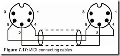
The connectors used are 5-contact DIN connectors, commonly utilized in the domestic audio equipment; a connecting cable schematics is shown in Fig. 7.17.
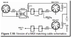
The external MIDI port (with TTL signals) is usually routed to the unused contacts (12 and 15) of the game adapter connector (DB-15S). To connect standard MIDI devices to this connector, a matching current loop-to-TTL adapter is needed, since the game card connector has TTL interface. A matching adapter is usually built into a special cable, one version of which is shown in Fig. 7.18. Some PCs have built-in adapters and standard 5-pin MIDI connectors.
In terms of software, the MIDI port is compatible with the MPU-401 UART. (The “MPU” stands for “MIDI Processing Unit”.) The Roland MPU-401 was the first MIDI interface PC expansion card to gain wide acceptance. In addition to the asynchronous serial port (UART) implementing the physical MIDI interface, this controller had well-developed hardware means to use the PC as a sequencer. The MPU-401 controller supported a simple operating mode, the UART mode, in which only the bidirectional asynchronous port was used; modern audio cards are compatible with the MPU-401 only in this mode.
In the I/O addressing space, the MPU-401 occupies two adjacent addresses: MPU (usually 330h) and MPU+1.
-
The DATA port (address MPU+0) is used to read and write bytes transmitted and received via the MIDI interface. In the smart mode, auxiliary data not related to the MIDI stream are also read via this port.
-
The STATUS/COMMAND port (address MPU+1) is used to read the status and write commands (writing can only be done in the smart mode). The following bits are defined in the status byte:
-
Bit 7—DSR (Data Set Ready). Received data are ready to be read when DSR=0. When all the data have been read out of the register, this bit is set to 1.
-
Bit 6—DRR (Data Read Ready). The UART is ready to write to the data or port register when DBR=0. If there is an unread data byte in the receiver, the ready condition cannot be set.
-
When powered up, a “true” MPU-401 card goes into the smart mode, from which it can be switched into the UART mode by the 3Fh command. The MPU-401 is reset (into the smart mode) by the RESET command (code FFh). The MPU-401 may confirm this command by generating an acknowledgement byte Ack (FEh). The acknowledge byte is extracted from the data register; until the MPU receives this byte, it will not accept following commands. The MPU does not acknowledge the 3Fh command (switch into the UART mode), although some emulators also confirm this command.
Data input can be implemented either by software polling the DSR bit, or by interrupts. In the UART mode, the MPU generates hardware interrupts upon receiving a byte. The interrupt handler must read out all the input data and terminates only upon ascertaining that DSR=1 (otherwise, some received bytes may be lost).
Data output is enabled by the DRR bit; no interrupt to send ready output data is generated.
MPU-401 compatibility, which most of the modern MIDI interface audio cards possess, means that a card must have a transceiver that is software compatible with MIDI in the UART mode; smart-mode functions are usually not supported.
In some motherboards, large-scale integration interface-controller microchips are used; these circuits’ UART mode, used for the COM port, can be switched into the MIDI port mode in BIOS Setup.
USB can be used to connect multiple MIDI devices to a PC. For this purpose, Roland, among others, produces a 64-channel S-MPU64 processor block that, in addition to the USB, has four input and four output MIDI ports. Software support allows up to four blocks to be joined on one USB bus, which increases the number of channels to 256.
7.5.4 Daughterboard Interface
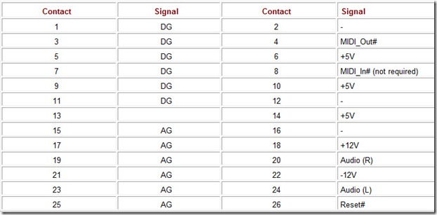
Several audio card models have an internal daughterboard connector for connecting a daughterboard with MIDI synthesizer. The MIDI port signal (TTL level, as for joystick connector) and the synthesizer hardware reset signal are routed from the main card to this connector (Table 7.19). The analog stereo signal is input from the daughterboard to this connector, to be farther relayed to the main card mixer. In the power supply circuits, the analog ground (AG) rail is separated from the digital ground (DG) rail. The MIDI input may also be used. The connector may be also be called a WT (Wavetable, Waveblaster) connector.
Table 7.19: Daughterboard Connector Contact Functions
Connecting a daughterboard is equivalent to connecting an external synthesizer to an audio card’s MIDI output. If the audio card does not have a daughterboard connector, the daughterboard can be connected to the external joystick/MIDI connector and to the audio card’s analog inputs. Of course, the power supply and reset must also be supplied to the daughterboard.
7.6 Game Port Interface
Gaming devices—joysticks, automobile steering wheels and pedals, and others—generate analog and digital signals that can be input to a computer. The game adapter interface (Game port), to which two joysticks or other devices could be connected, was introduced and virtually standardized in the first IBM PCs. Altogether, four coordinate variable-resistor sensors are available (X1, X2, Y1, and Y2) and four discrete control button inputs. The coordinate sensors’ roles depend on the particular game and the manipulator’s construction. In aircraft simulators, the X1 sensor may be responsible for tracking up/down movements of the control lever, the Y1 sensor for right/left movements, the X2 sensor for pressing the left or right pedal, and the Y2 sensor for the throttle lever. In automobile games, the X1 sensor tracks the steering wheel, the Y1 sensor the throttle pedal, and the X2 sensor the brake pedal (the throttle and the brake pedals may share the Y1 sensor). As well as entertainment purposes, the port may also be used to connect “serious” sensors.
Modern game devices have their own “brains”—a microcontroller—and are connected to the computer via a digital interface (either the USB bus or the COM port). Their functional capabilities are broader, and they allow the introduction of mechanical feedback to the player.
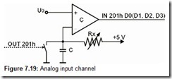
The Game port adapter has one register in the I/O address range. Its address is 201h, and its bits reflect the status of the buttons and analog signal comparators when read. How discrete button signals are input is obvious, and does not need to be explained. A simplified schematics of one analog input channel is shown in Fig. 7.19. At the beginning of the conversion, the capacitor discharges on the key, after which it starts charging. The rate of charging is determined by the value of the sensor’s resistance: The higher the resistance, the slower the charge. The voltage on the capacitor is controlled by the comparator, which is triggered upon reaching some certain threshold. The comparator outputs for all four conversion channels, as well as the discrete inputs, are collected into the register (see below) that can be read by software. The conversion is done purely by software, and begins when any byte has been output to the adapter register (201h); bits 0-3 are set to logical 1 at the beginning of this operation. Further, the program cyclically reads the adapter register and measures the time it takes bits 0-3 (which correspond to the four analog channels) to return to logical 0. If an analog input shorts to ground or a measured circuit is broken, the corresponding bit will not be zeroed out. Therefore, time-out provisions must be made in the conversion program. For resistors measured in the 0-100 K range, the time is calculated using the formula T(ms) = 24.2 + 11 × R(Kohm).
The precision and linearity of the conversion is not high, and the conversion itself is slow (taking up to 1.12 msec) and puts a heavy load on the processor. However, in contrast to “real” analog-to-digital converters, this one costs nothing: A game adapter is a part of practically all combined boards of parallel and serial ports and audio cards.
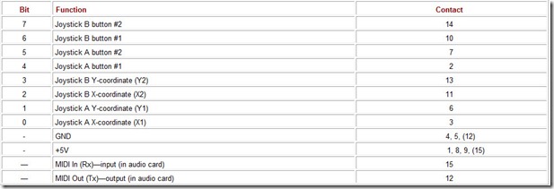
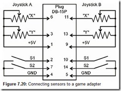
The port has a DB-15S female connector. The functions of the outputs and their corresponding register bits are shown in Table 7.20. The resistors are connected to the +5 V rail; the buttons are connected to the GND rail (Fig. 7.20.) Zeroes in bits 5-7 correspond to the closed button positions. The analog channels can be used to input discrete signals by connecting their inputs to buttons that link them to the GND rail, and to resistors that pull them up to +5 V. Two joysticks—A and B—can be connected using a Y-adapter. In audio cards, the game connector can be used along with joysticks to connect external MIDI devices by employing a special adapting cable that galvanically decouples the incoming signal and limits the incoming current (Fig. 7.18). The MIDI interface uses contacts 12 and 15, which used to be taken by GND and +5 V. This makes it safe to connect a MIDI adapter to a “pure” game port, and a usual joystick to a game port with MIDI signals.
Table 7.20: Game Adapter and MIDI Interface
Joystick system support is provided by the BIOS Int 15h service function 84h (AH=84h). When it is called, the subfunction number is loaded in the processor’s DX register:
-
DX=0—button monitoring. Returns button status into the AL[7:4] register (corresponds to port 201h bits).
-
DX=1—reading X, Y coordinates of the joystick A into the registers AX and BX and of the joystick B into the registers CX and DX.
When a wrong code is placed into the DX register, the CF is set to logical 1. The standard joystick is also supported by Windows.

![Table-7.2-Table-7.2.-Serial-Mouse-Co[2] Table-7.2-Table-7.2.-Serial-Mouse-Co[2]](http://machineryequipmentonline.com/electric-equipment/wp-content/uploads/2021/02/Table-7.2-Table-7.2.-Serial-Mouse-Co2_thumb.jpg)
![Figure-7.3-PS2-Mouse-Connector_thumb[2] Figure-7.3-PS2-Mouse-Connector_thumb[2]](http://machineryequipmentonline.com/electric-equipment/wp-content/uploads/2021/02/Figure-7.3-PS2-Mouse-Connector_thumb2_thumb.jpg)
![Figure-7.4-Bus-mouse-connector_thumb[1] Figure-7.4-Bus-mouse-connector_thumb[1]](http://machineryequipmentonline.com/electric-equipment/wp-content/uploads/2021/02/Figure-7.4-Bus-mouse-connector_thumb1_thumb.jpg)
![Figure-7.5-Data-transmission-using-t[1] Figure-7.5-Data-transmission-using-t[1]](http://machineryequipmentonline.com/electric-equipment/wp-content/uploads/2021/02/Figure-7.5-Data-transmission-using-t1_thumb.jpg)
![Table-7.3-Table-7.3.-Centronics-Inte[1] Table-7.3-Table-7.3.-Centronics-Inte[1]](http://machineryequipmentonline.com/electric-equipment/wp-content/uploads/2021/02/Table-7.3-Table-7.3.-Centronics-Inte1_thumb.jpg)
