Plasma operation
The principle of operation of a plasma pixel is closely related to that of the simple neon light. It has long been known that certain mixtures of gases such as neon, helium and xenon when subjected to a sufficiently strong electric voltage will break down into ‘plasma’ and what is known as plasma discharge occurs. Plasma is an electrically neutral, highly ionised substance consisting of electrons, positive ions and neutral particles. Being electrically neutral, it contains equal quantities of electrons and ions and is, by definition, a good conductor. Apart from conducting a current, plasma discharge converts a part of the electric energy into electromagnetic waves including ultra violet (UV) and visible light.
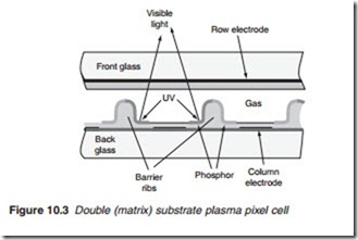
The first drawback of this simple plasma unit is the fact that the light emission from such a pixel is the familiar orange glow of neon signs. To overcome this, and produce colour, appropriate phosphors which emit dif- ferent colours when excited is used to cover the inside of the pixel. Ultraviolet rays generated by the discharge are then used to impact onto the phosphor coating to emit colour light as shown in Figure 10.3. To optimise the UV emission, the gas mixture is modified with the addition of xenon.
This process is used as the basis for a matrix of tiny pixel cells formed by an array of row and column electrodes placed within two glass substrates. In this type of construction, known as the matrix or double substrate plasma panel, the two electrodes are deposited in strips on two separate parallel glass plates with a discharge cell placed at each intersection.
This early design was modified to simplify manufacture, reduce cost and increase brightness. This is how the co-planar panel was born (Figure 10.4) in which the two electrodes, scan (Y) and common sustain (X or C) are placed on the same plane rather than facing each. The discharge thus occurs between two electrodes which are parallel to each other and are deposited on the same glass plate. A third electrode, the address or data electrode is added to ensure the discharge takes place perpendicular to the parallel electrodes and to determine which cell will suffer a discharge.
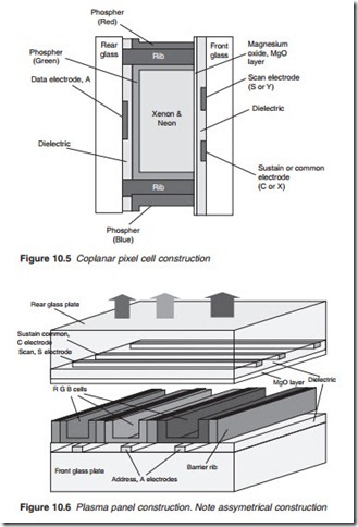
Figure 10.5 shows the construction of a coplanar pixel cell. The cells are separated by barrier ribs to prevent electrical and optical interaction (crosstalk) between the cells. The inside walls of the ribs are covered with a layer of phosphor. The electrodes are deposited on the front and rear glass plates: scan and sustain electrodes on the front and the address electrodes on the rear. The dielectric layer above the electrodes which is typically 20–25 Jlm thick protects the electrodes and provides a capacitive reactance in series with the cell which apart from acting as a current limiter, is crucial to the formation of the wall charge which acts as a tem- porary memory storing one-bit video data. This is followed by the MgO (Magnesium Oxide) layer to protect the dielectric. Its large secondary electron emission coefficient when bombarded by neon or helium ions helps to maintain a low plasma breakdown voltage. The final layer is the phosphor layer responsible for light emission.
The panel is constructed by first mounting the address electrodes on the rear glass (Figure 10.6). A protective coating of a dielectric is then added. Ribs are formed as dividers and colour phosphors are then added to the cells. Scan and Sustain transparent electrodes are mounted on the front glass and coated with a protective dielectric. Finally an MgO overcoat is
applied on the front glass for protection of electrodes from the discharge. The scan and sustain electrodes occupy a large area on the front glass plate and therefore must be transparent. Indium tin oxide, ITO is used for that purpose. Due to the resistivity of ITO, a small metal electrode, a bus electrode, is generally deposited on the edge of each coplanar electrode to maintain a constant voltage along the electrode. The two plates are then sealed and plasma gas, e.g. Xenon in Neon or Helium are pumped at a pressure lower than normal atmospheric sea level. In this way, the two glass plates are constantly under external pressure thus sustaining the seal.
From this basic structure, Red, Green and Blue colour are produced. It will be noticed from Figure 10.6 that the pixel cells have different sizes with the blue cell being the largest and the red cell smallest. The reason for this asymmetric cell structure is that blue makes a greater contribution to colour temperature and when blue is brighter, it is possible to use brighter red and green so that the panel as a whole is brighter. However, the asymmetric arrangement has the major disadvantage of increasing manufacturing costs and reducing lifetime. For this reason, some manufacturers have opted to the symmetrical phosphor arrangement with appropriate changes to the video signal to counter the varied colour contribution of primary colours.
The life time of a display is mainly limited by the sputtering of the MgO layer. Although the secondary emission properties of MgO do not change significantly even after hundreds of nanometers are removed from its sur- face by sputtering, its life time is limited, typically 50,000 or 60,000 h at average brightness.


