Low-voltage differential signalling
The LVDS protocol is a unidirectional digital data connection which encodes 24 bits of data using four differential serial data pairs (each pair consists of two twisted wires). The pixel clock is transmitted on a separate differential pair. The differential swing is low (355 mV) and the nominal impedance is 100–120 Q with a speed of 500 Mbps to 1.5 Gbps (Figure 16.4).
Parallel data are fed into an LVDS transmitter which encodes the incoming data into four serial channels to be sent out on four separate data pairs of wires. The data pairs are not dedicated to any specific part of the video signal with each one transmitting bits from all RGB components. The clock is sent out on a separate pair as shown. At the other end, a LVDS receiver is necessary to decode the data back to its original format or another format as necessary.
The LVDS clock rate is 7X the original pixel clock; the pixel clock being the rate at which the pixels are addressed. Given that bits are sent at the LVDS clock rate, then 7 bits are sent every pixel clock pulse. With four LVDS channels, the number of bits per LVDS clock pulse is 4 X 7 = 28 bits. Of these, 24 are used for video. Of the remaining four bits, one bit is allo- cated to each of the following: frame sync, line sync and display enable (DE). The final bit is a ‘custom’ bit that may be used by the manufacturer as required for the particular application.
For a basic 24-bit video, a 65 MHz connection can support a standard VGA-resolution panel. Capacity may be increased using an additional four channels, making a total of eight. This is known as dual-channel LVDS. Each channel can carry a 24-bit video.
LVDS achieves high aggregated bandwidth, low power consumption and low EMI by virtue of its low switching voltages, soft transition and true differential data transmission.
Figure 16.5 shows a typical LVDS transmitter/encoder chip. The 24-bit video input, H and V syncs and Enable fed into pins marked IN0–IN23. The allocation is as shown with R0 to IN27 (pin 50), R1–R4 to IN1–IN4 (pins 52, 54–56), R7 to IN5 (pin2), R5 to IN6 (pin 3) and so on for the remaining R, G and B bits. Hsync to IN24 (pin 27) and Vsync to IN25 (pin 28) with the bit clock (BLK) to IN26 (pin 30) and finally Enable (PRT) to IN23 (pin 25). The output is a four data differential pairs marked OUT0+ and OUT0- (pins 47 and 48), OUT1+ and OUT1- (pins 45 and 46)
and so on, and a clock pair marked CLKOUT+ and CLKOUT- (pins 39 and 40).
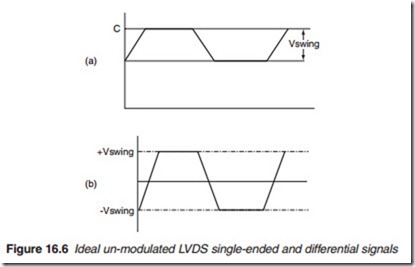
The ideal waveform of a single-ended differential signal, representing either the positive or negative terminal of a differential pair, is in Figure 16.6a. Since the signal is differential, the net signal on the pair has a swing twice that of the single ended as illustrated in Figure 16.6b. The amplitude is in the region of 300–400 mV. The repetition frequency will depend on the LVDS clock which typically is 60 and 80 MHz for standard and high- definition television respectively. This is a good test to see if the LVDS transmitter is functioning normally in no video on the screen.
When video data is transmitted, the LVDS swing is modulated result- ing in the waveform shown in Figure 16.7. A typical clock waveform is shown in Figure 16.8.
To observe this differential waveform, an isolated double-beam oscillo- scope must be used with its inputs connected to the two data pair wires and their earths shorted.
LDVS point-to-point transmission is suitable for short distances of up to 1 m. For longer cabling, other interface protocols must be used such as PanelLink and TMDS.

