The Instruction Set of 8086

The Instruction Set of 8086

1. How many instructions are there in the instruction set of 8086? Ans. There are 117 basic instructions in the instruction set of 8086.

2. Do 8086 and 8088 have the same instruction set? Ans. Yes, both 8086 and 8088 have the same instruction set.

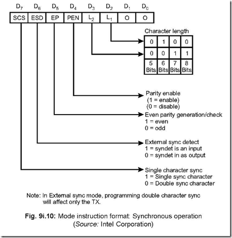
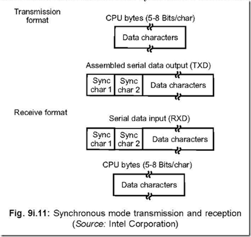
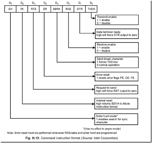
3. Mention the groups in which the instruction set of 8086 can be categorised. Ans. The instruction set of 8086 can be divided into the following number of groups,

namely:

z Data transfer instructions

z Arithmetic instructions

z Logic instructions

z Shift instructions

z Rotate instructions

z Flag control instructions

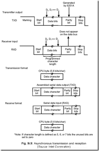
z Compare instructions

z Jump instructions

z Subroutines and subroutine handling instructions

z Loop and loop handling instructions

z Strings and string handling instructions.

4. Mention the different types of data transfer instructions. Ans. The different types include:

z Move byte or word instructions (MOV)

z Exchange byte or word instruction (XCHG)

z Translate byte instructions (XLAT)

z Load effective address instruction (LDA)

z Load data segment instruction (LDS)

z Load extra segment instruction (LES)

5. Can the MOV instruction transfer data directly between a source and destination that both reside in external memory?

Ans. No, it cannot. With the first MOV instruction, data from the source memory is to be moved into an internal register-normally accumulator. The second MOV instruction places the accumulator content into the destination memory.

6. Explain the following two examples:

(a) MOV CX, CS

(b) MOV AX, [ALPHA]

Ans. (a) MOV CX, CS: It stands for, “move the contents of CS into CX”. If CS contains 1234 H, then on execution of this instruction, content of CX would become 1234 H i.e., content of CH = 12 H and Content CL = 34 H.

(b) MOV AX, [ALPHA]: Let, data segment register DS contains 0300 H and ALPHA

corresponds to a displacement of 1234 H. Then the instruction stands for, “move the content of the memory location offset by 1234 H from the starting location 0300 H of the current data segment into accumulator AX”. The physical address is

PA = 03000 H + 1234 H = 04234 H

Thus execution of the instruction results in content of memory location 04234 H is moved to AL and content of memory location 04235 H is moved to AH.

7. Show the forms of XCHG instruction and its allowed operands. Ans. These are shown below in Fig. 14.1

Mnemonic

Meaning

Format

Operation

Flags affected

XCHG

Exchange

XCHG D,S

(D)↔(S)

None

(a)

Destination

Source

Accumulator

Memory

Register

Reg16

Register

Register

(b)

Fig.14.1: (a) Exchange data transfer instruction (b) Allowed operands

8. Explain the instruction XCHG BX, CX.

Ans. The execution of this instruction interchanges the contents of BX and CX, i.e., original content of CX moves over to BX and original content of BX moves over to CX.

9. Explain XLAT instruction.

Ans. The translate (XLAT) data transfer instruction is shown in Fig.14.2. It can be used for say an ASCII to EBCDIC code conversion.

Mnemonic

Meaning

Format

Operation

Flags affected

XLAT

Translate

XLAT

((AL)+(BX)+(DS)O)→(AL)

None

Fig.14.2: Translate data transfer instruction

The content of BX represents the offset of the starting address of the look up table from the beginning of the current data segment while the content of AL represents the offset of the element which is to be accessed from the beginning of the look up table.

As an example, let DS = 0300 H, BX = 1234 H and AL = 05 H. Hence, PA = 03000 H + 1234 H + 05 H = 04239 H

Thus, execution of XLAT would put the content of 04239 H into AL register.

Conceptually, the content of 04239 H in EBCDIC should be the same as the ASCII

character equivalent of 05 H.

10. Explain the instruction LEA, LDS and LES.

Ans. These three instructions are explained in Fig.14.3. These instructions stand for load register with effective address (LEA), load register and data segment register (LDS) and load register and extra segment register (LES) respectively..

The Instruction Set of 8086 6-18-09 PM

LEA instruction loads a specified register with a 16-bit offset value. LDS and LES instructions load the specified register as well as DS or ES segment register respectively. Thus a new data segment will be activated by a single execution.

11. Indicate the different types of arithmetic instructions possible with 8086.

Ans. The different arithmetic instructions are addition, subtraction, multiplication and division and are shown in Fig.14.4.

Addition

ADD

Add byte or word

ADC

Add byte or word with carry

INC

Increment byte or word by 1

AAA

ASCII adjust for addition

DAA

Decimal adjust for addition

Subtraction

SUB

Subtract byte or word

SBB

Subtract byte or word with borrow

DEC

Decrement byte or word by 1

NEG

Negate byte or word

AAS

ASCII adjust for subtraction

DAS

Decimal adjust for subtraction

Multiplication

DIV

Divide byte or word unsigned

IDIV

Integer divide byte or word

AAD

ASCII adjust for division

CBW

Convert byte to word

CWD

Convert word to double word

Fig.14.4: Arithmetic instructions

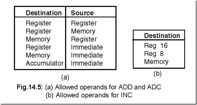
12. Show the allowed operands for the instruction ADD, ADC and INC.

Ans. The allowed operands for ADD and ADC are shown in Fig.14.5 (a) and for INC it is shown in Fig.14.5 (b).

The Instruction Set of 8086 6-18-58 PM

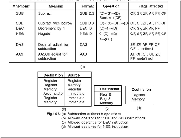
13. Show the different subtraction arithmetic instructions. Also show the allowed operands for (a) SUB and SBB (b) DEC and (c) NEG instructions.

Ans. The different subtraction arithmetic instructions and the allowed operands, for the different instructions are shown in Fig. 14.6 (a), (b), (c) and (d) respectively.

The Instruction Set of 8086 6-19-20 PM

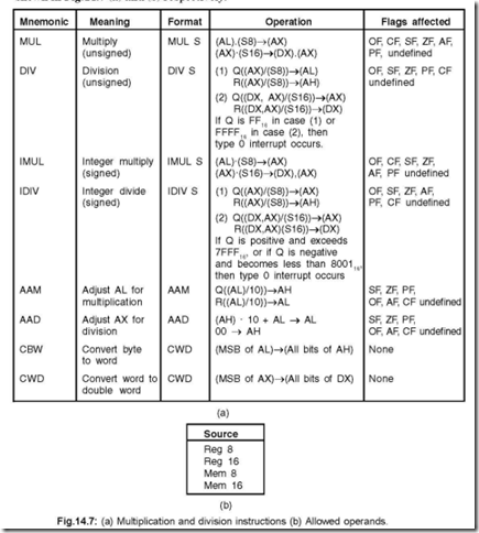
14. Show the different multiplication and division instructions and also the allowed operands.

Ans. The different multiplication and division instructions and also the allowed operands are shown in Fig.14.7 (a) and (b) respectively.


The Instruction Set of 8086 6-19-59 PM


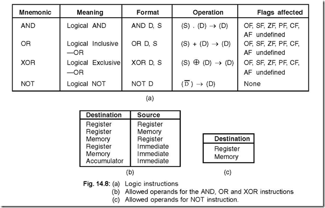
15. Show the different logic instructions and also the allowed operands for

(a) AND, OR and XOR (b) NOT instructions.

Ans. The different logic instructions as also the allowed operands for different instructions are shown in Fig.14.8 (a), (b) and (c) respectively.

The Instruction Set of 8086 6-20-25 PM_thumb

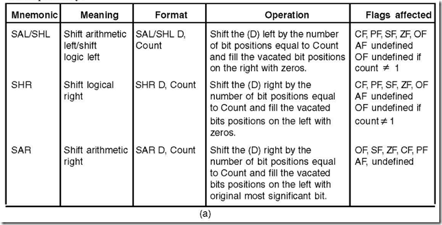
16. What are the two basic shift operations?

Ans. The two basic shift operations are logical shift and arithmetic shift.

The two logical shifts are shift logical left (SHL) and shift logical right (SHR), while

the two arithmetic shifts are shift arithmetic left (SAL) and shift arithmetic right (SAR).

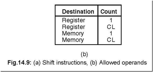
17. Show the different shift instructions and the allowed operands.

Ans. The various shift instructions and the allowed operands are shown in Fig. 14.9 (a) and

(b) respectively.

The Instruction Set of 8086 6-20-57 PM_thumbThe Instruction Set of 8086 6-21-17 PM_thumb

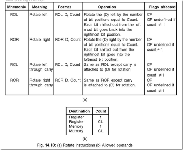
18. Show the different Rotate instructions and the allowed operands.

Ans. The different Rotate instructions and the allowed operands are shown in Fig. 14.10 (a) and (b) respectively.

The Instruction Set of 8086 6-21-43 PM_thumb

19. Name the different flags control instructions, the operations performed by them and also the flags affected.

Ans. Fig. 14.11 shows the different flags control instructions, their meaning and the flags affected by respective instructions.

Mnemonic

Meaning

Operation

Flags affected

LAHF

Load AH from flags

(AH) ← (Flags)

None

SAHF

Store AH into flags

(Flags) ← (AH)

SF, ZF, AF, PF, CF

CLC

Clear 0carry flag

(CF) ←

CF

STC

Set ca1rry flag

(CF) ←

CF

CMC

Complement carry flag

(CF) ← (CF)

CF

CLI

Cle0ar interrupt flag

(IF) ←

IF

STI

Se1t interrupt flag

(IF) ←

IF

clip_image003_thumbFig. 14.11: Flag control instructions

20. Which register plays an important part in flag control instructions?

Ans. It is the accumulator register AH which plays an important part in flag control instructions.

For instance, if the present values in the flags are to be saved in some memory location then they are first to be loaded in the AH register and transfered to memory location, say M1, i.e.,

LAHF → Load AH from flags

MOV M1, AH → Move contents of AH into memory location M1.

As a second example, if the content of memory location, Say M2, is to be placed into flags, then

MOV AH, M2 → Move contents of memory location M2 into AH register.

SAHF → Store AH into flags.

21. List the characteristics of CMP instructions.

Ans. The following are the characteristics of CMP instruction:

z Can compare two 8-bit or two 16-bit numbers.

z Operands many reside in memory, a register in the CPU or be a part of an instruction.

z Results of comparison is reflected in the status of the six status flags—CF, AF, OF, PF, SF and ZF.

z CMP is a subtraction method—it uses 2’s complement for this.

z Result of CMP is not saved—but based on CMP result, appropriate flags are either set/reset.

22. Explain CMP instruction.

Ans. The compare instruction, different operand combinations and the flags affected are shown in Fig. 14.12.

Mnemonic

Meaning

Format

Operation

Flags affected

CMP

Compare

CMP D, S

(D) – (S) is used in setting or resetting the flags

CF, AF, OF, PF, SF, ZF

(a)

Destination

Source

Register Register Memory Register Memory Accumulator

Register Memory Register Immediate Immediate Immediate

(b)

Fig.14.12: (a) Compare instruction (b) Operand combination

23. What are the two basic types of unconditional jumps? Explain.

Ans. The two basic types of unconditional jumps are intrasegment jump and intersegment jump.

The intrasegment jump is a jump for which the addresses must lie within the current

code segment. It is achieved by only modifying the value of IP.

The intersegment jump is a jump from one code segment to another. For this jump

to be effective, both CS and IP values are to be modified.

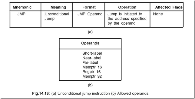
24. Show the unconditional jump instructions and the allowed operands.

Ans. The unconditional jump instruction, along with the allowed operands are shown in Fig.

14.13 (a) and (b) respectively.

The Instruction Set of 8086 6-22-56 PM_thumb

Jump instructions carried out with a Short-label, Near-label, Memptr 16 or Regptr 16 type of operands represent intrasegment jumps, while Far-label and Memptr 32 represent intersegment jumps.

25. Distinguish between Short-label and Near-label jump instructions. Ans. The distinction between the two is shown in a tabular form.

The Instruction Set of 8086 6-23-14 PM_thumb

26. Describe the Memptr 16 and Regptr 16 jump instructions.

Ans. Both these types permit a jump to any location (address) in the current code segment.

Again the contents of a memory or register indirectly specifies the address of the jump,

as the case may be.

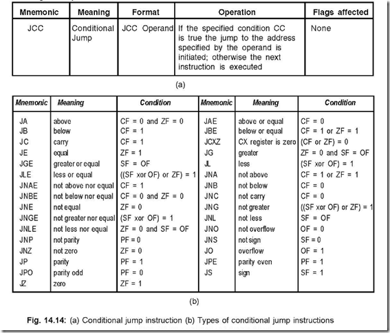
27. Show the conditional jump instruction and their different types.

Ans. The conditional jump instruction and their different types are shown in Fig. 14.14 (a) and

(b) respectively.

The Instruction Set of 8086 6-23-35 PM_thumb

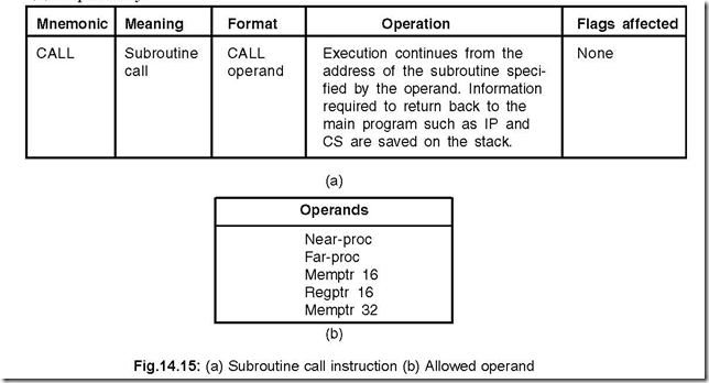
28. Show the subroutine CALL instruction and the allowed operands.

Ans. The CALL instruction and the allowed operands are shown in Fig.14.15(a) and

(b) respectively.2929.The Instruction Set of 8086 6-23-58 PM_thumb
29.What are the two types of CALL instructions? Discuss.

Ans. The two types are: intrasegment CALL and intersegment CALL.

If the operands are Near-proc, Memptr16 and Regptr16, then they specify intrasegment

CALL while Far-proc and Memptr32 represent intersegment CALL.

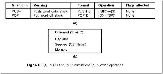
30. Show the PUSH and POP instructions, as also the allowed operands.

Ans. The PUSH and POP instructions, as also the allowed operands are shown in Fig.14.16

(a) and (b) respectively.

The Instruction Set of 8086 6-24-19 PM_thumb

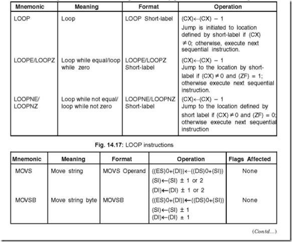
31. How many loop instructions are there and state their use.

Ans. There are in all three loop instructions. They can be used in place of certains conditional jump instructions. These instructions give the programmer a certain amount of flexibility in writing programs in a simpler manner.

32. List the different instructions and also the operations they perform.

Ans. The different loop instructions and the operations they perform are shown in Fig. 14.17.

33. What is meant by a ‘string’ and what are the characteristics of a string instruction?

Ans. A string is a series of data words (or bytes) that reside in successive memory locations.

The characteristics of a string instruction are:

z Can move data from one block of memory locations to another one.

z A string of data elements stored in memory can be scanned for a specific data value.

Successive elements of two strings can be compared to determine whether the two

strings are same/different.

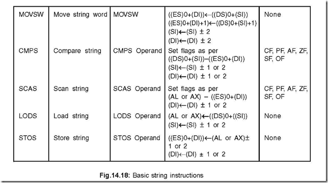
34. List the basic string instructions and the operations they perform.

Ans. The basic string instructions and the operations they perform are shown in Fig. 14.18

The Instruction Set of 8086 6-24-40 PM_thumbThe Instruction Set of 8086 6-24-57 PM_thumb

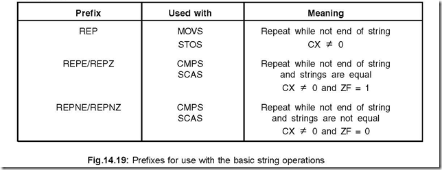
35. What is a ‘REP’ instruction? Discuss.

Ans. ‘REP’ stands for repeat and is used for repeating basic string operations—required for processing arrays of data.

There are a number of repeat instructions available and are used as a prefix in string instructions. The prefixes for use with the basic string instructions are shown in Fig. 14.19.

The Instruction Set of 8086 6-25-17 PM_thumb

36. Discuss the instructions for Autoindexing of string instructions.

Ans. When the system executes some string instruction, the addresses residing in DI and SI are incremented/decremented automatically. The content of direction flag (DF) decides the above. Two instructions—CLD (clear DF flag) or STD (Set DF flag) are used for the above and shown in Fig. 14.20.The Instruction Set of 8086 6-25-36 PM_thumb[1]

Fig. 14.20: Instructions for autoincrementing and autodecrementing in string instructions

Execution of CLD (this makes DF = 0) permits autoincrement mode while execution of STD (this makes DF = 1) permits autodecrement mode.

SI or DI are autoincremented/autodecremented by one if a byte of data is processed or by two if a word of data is processed.

37. Write down the equivalent string instructions for the following two.

(i) MOV AL, [DI]

(ii)

MOV AL, [SI]

CMP AL, [SI]

DEC SI

MOV [DI], AL INC SI

DEC DI

INC DI

Ans. The following two are the equivalent string instructions of the given ones:

(i) STD (ii) CLD

CMP SB MOV SB

38. Where do memory source and destination addresses reside in string instructions?

Ans. The memory source and destination addresses in such cases are register SI in the data segment and DI in the extra segment.

 

Programming Techniques

Programming Techniques

1. Write an ALP (assembly language programming) for addition of two 8-bit data BB H and 11 H.

Ans. 0200 MOV AL, BB H : 8-bit data BB H into AL 0202 MOV CL, 11 H : 8-bit data 11 H into CL

0204 ADD AL, CL : Contents of AL and CL added

0206 HLT : Stop.

Comment : Result in AL = CC H.

2. Write an ALP for addition of two 16-bit data BB11 H and 1122 H. Ans. 0200 MOV AX, BB11 H : 16-bit data BB11 H into AX

0203 MOV CX, 1122 H : 16-bit data 1122 H into CX

0206 ADD AX, CX : Contents of AX and CX added

0208 HLT : Stop

Comment : Result in AX = CC33 H.

3. Write an ALP for addition of two 8-bit data BB H and 11 H. The first data has an offset address of 0304 H and displacement.

Ans. 0200 MOV BX, 0304 H : Offset address put in BX 0203 MOV AL, 11 H : 8-bit data 11H into AL

0205 ADD AL, [BX + 07] : 8-bit data from offset + displacement added with AL 0207 HLT : Stop.

Comment : Result in AL = CC H.

4. Write an ALP that subtracts 1234 H existing in DX from the word beginning at memory location MEMWDS.

Ans. 0200 MOV DX, 1234 H : 16-bit data 1234 H put into DX

0203 SUB MEMWDS, DX : Subtract data word 1234 H existing in DX from the data

word pointed to by MEMWDS.

0208 HLT : Stop.

Comment : If MEMWDS points to 3000 H then,

[3001 H : 3000 H] ← [3001 H : 3000 H] – 1234 H

5. Write an ALP which multiplies two 8-bit data 21 H and 17 H. Ans. 0200 MOV AL, 21 H : 8-bit multiplicand 21 H put into AL

0202 MOV CL, 17 H : 8-bit multiplier 17 H put into CL

0204 MUL CL : Contents of CL and AL are multiplied and the result

stored in AX

0206 HLT : Stop.

Comment : Result in AX = 02F7 H.

6. Write an ALP for dividing 1234 H by 34 H.

Ans. 0200 MOV AX, 1234 H : 16-bit dividend in 1234 H 0203 MOV CL, 34 H : 8-bit divisor in 34 H

0205 DIV CL : Content of AX divided by content of CL

0207 HLT : Stop.

Comment: Result in AX with

Quotient in AL = 59 H and

Remainder in AH = 20 H.

7. Write ALP that saves the contents of 8086’s flags in memory location having an offset 1212 H and then to reload the flags from the contents of the memory location having an offset 2121 H.

Ans. 0200 LAHF : Load AH from flags

0201 MOV [1212], A H : Move the contents of AH to memory locations pointed to

by offset 1212 H

0205 MOV AH, [2121] : Move the contents of memory locations pointed to offset

2121 H to AH

0209 SAHF : Store AH into flags

020A HLT : Stop.

8. Write an ALP that transfers a block of 100 bytes of data. The source and destination memory blocks start at 3000 H and 4000 H memory locations respectively. The data segment register value is DSADDR.

Ans. 2000 MOV AX, DSADDR : Move initial address of DS register into AX.

2003 MOV DS, AX : DS loaded with AX

2005 MOV SI, 3000 H : Source address put into SI.

2008 MOV DI, 4000 H : Destination address put into DI.

200B MOV CX, 64 H : Count value for number of bytes put into CX register

200D MOV AH, [SI] : Source byte moved into AH

200F MOV [DI], AH : AH byte moved into destination address

2011 INC SI : Increment source address

2012 INC DI : Increment destination address

2013 DEC CX : Decrement CX count

2014 JNZ 200D : Jump to 200D H until CX = 0

2017 HLT : Stop.

9. Write an ALP for ASCII addition of two numbers 2 H and 5 H.

Ans. 2000 MOV AL, 32 H : ASCII code 32 H for number 2 H is moved into AL 2002 MOV BL, 35 H : ASCII code 35 H for number 5 H is moved into BL 2004 AAA : ASCII adjust for addition

2005 HLT : Stop.

Result : (AL) = 07 H.

10. Write an ALP to find the average of two numbers. Ans. 2000 MOV AL, 72 H : Get 1st number 72 H in AL

2002 ADD AL, 78 H : Add 2nd number 78 H with 72 H (in AL)

2004 ADC AH, 00 H : Put the carry in AH

242 Understanding 8085 Microprocessor and Peripheral ICs through Problems and Solutions

2006 SAR AX, 1 : Divide Sum by 2

2008 MOV [3000 H], AL : Copy AL content in memory location 3000 H 200B HLT : Stop.

11. Write an ALP for moving a block consisting of 10 bytes from memory locations starting from 5000 H to memory locations starting from 6000 H. Use LOOP instruction.

Ans. 2000 CLD : Clear direction flag 2001 MOV SI, 4000 H : Source address put in SI

2004 MOV DI, 5000 H : Destination address put in DI

2007 MOV CX, 000A H : Put number of bytes to be transferred in CX.

200A MOV SB : 1 byte copied from memory addressed by SI to addressed

by DI.

200B LOOPNZ 200A H : Loop till CX = 0

200D HLT : Stop.

12. Write an ALP to find 2’s complement of a string of 100 bytes. Ans. 2000 CLD : Clear direction flag

2001 MOV SI, 4000 H : Source address put in SI

2004 MOV DI, 5000 H : Destination address put in DI

2007 MOV CX, 0064 H : Put the number of bytes to be 2’s complemented in CX 200A LODSB : Data byte to AL and INC SI

200B NEGAL : 2’s Complement of AL

200D STOSB : Current AL value into DI and INC DI 200E LOOPNZ 200A H : Loop till CX = 0.

2010 HLT : Stop.

13. Write an ALP for block move of 100 bytes using Repeat instruction. Ans. 2000 CLD : Clear direction flag

2001 MOV SI, 4000 H : Source address put in SI

2004 MOV DI, 5000 H : Destination address put in DI

2007 MOV CX, 0064 H : Put number of bytes to be block moved into CX 200A REPNZ : Repeat till CX = 0

200B MOVSB : Move data byte addressed by SI to DI.

2009 HLT : Stop.

14. Write an ALP to evaluate X (Y + Z), where X = 10 H, Y = 20 H and Z = 30 H.

Ans. 2000 MOV AL, 20 H : 20 H put in AL 2002 MOV CL, 30 H : 30 H put in CL

2004 ADD AL, CL : AL and CL are added up and result in AL 2006 MOV CL, AL : AL transferred in CL

2008 MOV AL, 10 H : 10 H put in AL

200A MUL CL : AL and CL are multiplied and result in AL 200C MOV SI, 4000 H : Source address in SI

200F MOV SI, AL : AL put in SI

2011 HLT : Stop.

15. Write an ALP that reverses the contents of the bytes TABLE through TABLE + N – 1.

Ans. 2000 MOV CL, N : Number N put in CL 2002 MOV CH, 00 H : 00 H put in CH

2004 MOV SI, TABLE : Starting address of TABLE put in SI 2007 MOV DI, SI : DI loaded with SI value

2009 SUB DI, 01 : 01 subtracted from DI

200B ADD DI, CX : CX value added to present DI value 200D SHR CX, 01 : Divide CX count value by 2

200F MOV AL, [SI] : Move data pointed to by SI into AL 2011 XCHG AL, [DI] : Exchange AL with data pointed to by DI 2013 MOV [SI], AL : Save the exchanged data in SI

2014 INC SI : Increment SI

2015 DEC DI : Decrement DI

2016 LOOP 200F H : Continue till CX = 0

2019 HLT : Stop.

16. Write an ALP to find the maximum value of a byte from a string of bytes. Ans. 2000 MOV SI, 3000 H : Source address put in SI

2003 MOV CX, 0100 H : Count value of bytes put in CX

2006 MOV AH, 00 H : AH initialised with 00H

2008 CMP AH, [SI] : AH compared with data pointed to by SI 200A JAE 200E H : Jump if AH is ≥ (SI) to 200E H

200C MOV AH, [SI] : Otherwise, move (SI) to AH 200E INC SI : Increment SI

200F LOOPNZ 2008 : Loop unless CX ≠ 0

2011 MOV [SI], AH : (AH) transferred to the memory location pointed to by SI 2013 HLT : Stop.

17. Write an ALP to find the minimum value of a byte from a string of bytes. Ans. 2000 MOV SI, 3000 H : Source address put in SI

2003 MOV CX, 0100 H : Count value of bytes put in CX

2006 MOV AH, 00 H : AH initialised with 00H

2008 CMP AH, [SI] : AH compared with data pointed to by SI 200A JB 200E H : Jump if (AH) < (SI) to 200E H

200C MOV AH, [SI] : Otherwise move (SI) to AH

200E INC SI : Increment SI

200F LOOPNZ 2008 : Loop unless CX ≠ 0

2011 MOV [SI], AH : (AH) transferred to the memory location pointed to by SI 2013 HLT : Stop.


Addressing Modes of 8086

Addressing Modes of 8086

1. What is meant by addressing mode?

Ans. An instruction consists of an opcode and an operand. The operand may reside in the accumulator, or in a general purpose register or in a memory location.

The manner in which an operand is specified (or referred to) in an instruction is called addressing mode.

2. Name the different addressing modes of 8086.

Ans. The following are the different addressing modes of 8086:

z Register operand addressing.

z Immediate operand addressing.

z Memory operand addressing.

3. Mention the different memory addressing modes. Ans. The different memory addressing modes are:

z Direct Addressing

z Register Indirect Addressing

z Based Addressing

z Indexed Addressing

z Based Indexed Addressing and

z Based Indexed with displacement.

4. How the physical address is generated for the different memory addressing modes?

Ans. Physical address (for the operand) is the address from which either a read or write operation is initiated. The following shows the manner of generation of physical address.

Physical address

=

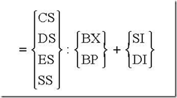
Segment base : Effective address

=

Segment base : Base + Index + Displacement

Addressing Modes of 8086 5-17-12 PM

i.e., effective address, for its generation, can have as many as three elements: Base, Index and Displacement. Thus the effective address is generated from the following:

Effective address = Base + Index + Displacement

The segment registers can be CS, SS, DS or ES. Base can be BX or PB. Index can be SI or DI and the Displacement can either be 8-bit or 16-bit.

It should be noted that not all the three elements viz., base, index or displacement are always used for effective address calculations.

5. Give examples each of (a) Register Addressing mode (b) Immediate Addressing mode.

Ans. (a) Register Addressing Mode.

In this mode, either an 8-bit or a 16-bit general purpose register contains the operand. Some examples are:

MOV AX, BX

MOV CX, DX

ADD AL, DH

ADD DX, CX

The content of BX register is moved to AX register in the first example, while in the third example, content of DH is added to the content of AL. Here, source and destination of data are CPU registers.

(b) Immediate Addressing Mode.

In this mode, the operand is contained in the instruction itself, i.e., the operand forms a part of the instruction itself. The operand can be either 8-bit or 16-bit in length. Some examples are:

MOV AL, 83 H

ADD AX, 1284 H

In the first example, 83 H is moved to AL register while in the second example, 1284 H is added to the contents of AX register. Here, source of data is within the instruction.

6. Discuss the Direct Addressing Mode.

Ans. In a way it is similar to ‘Immediate Addressing Mode’. In Immediate Addressing Mode, data follows the instruction opcode, while in this case an effective address follows the same. Thus in this case:

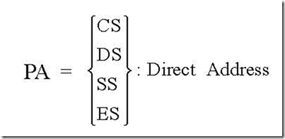
PA = Segment base : Direct address.

By default, the segment base register is DS. Thus,

PA = DS : EA

But if a segment override prefix (SEG) is used in the instruction, then any one of the four segment registers can be referenced. Hence, in general,

Addressing Modes of 8086 5-17-42 PM

As an example, MOV CX, [ALPHA]

It means, “move the contents of the memory location, which is labelled as ALPHA in the current data segment, into register CX”.

Thus, if DS = 0300 H, and value assigned to ALPHA is 3216 H, then

PA = 03000 H + 3216 H

= 06216 H

Thus, data contained in address locations 06217 H and 06216 H will be stored in CH and CL registers respectively.

MOV [0404 H], CX would move the contents of CL to offset address 0404 H (relative to data segment register DS) and CH to 0405 H. Here, memory address is supplied within the instruction.

7. Discuss Register Indirect Addressing Mode.

Ans. In a way, this mode of addressing is similar to direct addressing mode in the sense that content of DS is combined with the effective address to get the physical address.

But the difference lies in the manner in which the offset is specified. In direct addressing mode EA is constant while in this mode EA is a variable.

EA can reside in either base register (BX or BP) or index register (SI or DI). The

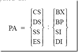
default segment register is DS, but again by using a segment override prefix (SEG), any of the four segment registers can be referenced. Thus, PA can be computed as:

10-25-2014 5-25-20 PM

An instruction of this mode of addressing is:

MOV CX, [SI]

Execution of this instruction entails moving the content of the memory location having its offset value in SI from the beginning of the current data segment to the CX register.

If DS = 0300 H and SI = 3216 H, then PA becomes

PA = 03000 H + 3216 H = 06216 H.

Thus data contained in 06217 H and 06216 H will be placed in CH and CL registers respectively. Here, memory address is supplied in an index or pointer register.

8. Discuss Based Addressing Mode.

Ans. The physical address in this case is generated as follows:

PA = Segment base: Base + DisplacementAddressing Modes of 8086 5-18-14 PM

i.e., the physical address is generated by adding either an 8-bit or 16-bit displacement to the contents of either base register BX or base pointer register BP and the current value in DS or SS respectively.

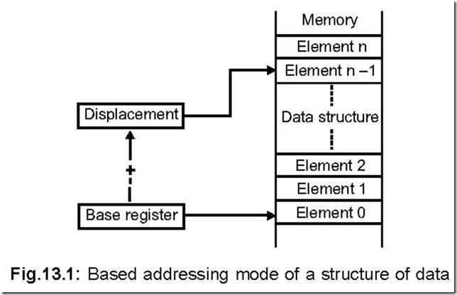
Fig. 13.1 shows the utility of using either BX/BP and displacement. The figure shows a data structure starting from ‘Element 0’ to ‘Element n’. Inserting a zero value for displacement would ensure accessing ‘Element 0’ of the structure. For accessing different elements within the same data structure, all that is to be done is to change the value of displacement.

Whereas, to access the same element is another data structure the value of the base register has to be changed, keeping the value of displacement same as before.

Addressing Modes of 8086 5-18-54 PM

An example of this mode of addressing is MOV [BX] + ALPHA, AH

Here, ALPHA denotes displacement (which can be 8 or 16-bits) and BX the base register. Together, they give EA of the destination operand.

If DS = 3000 H, BX = 1234 H and displacement (16-bit) = 0012 H, Then, PA = 03000 H + 1234 H + 0012 H = 04246 H

Thus the content of AH (source operand) is placed in the physical address 04246 H (destination operand memory location).

In this mode also, the default register i.e., DS can be changed by a segment override

prefix (SEG). Also for accessing data from the stack segment of the memory, BP is to be used instead of BX.

Here, the memory address is the sum of BX or BP base registers plus an 8 or 16-bit displacement specified in the instruction.

9. Discuss Indexed Addressing Mode.

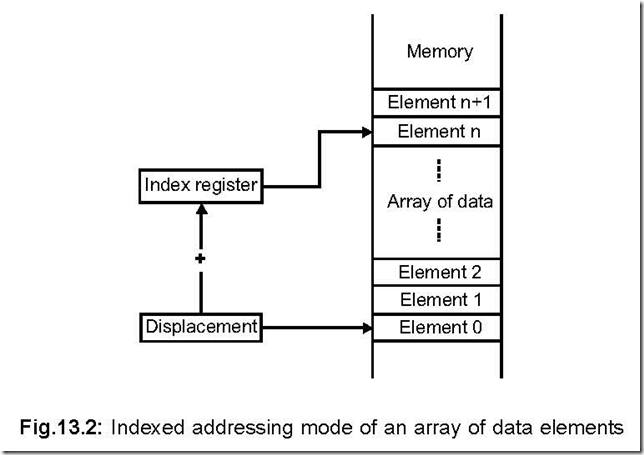
Ans. In a way, this mode of addressing is similar to the based addressing mode but the jobs carried out by base register and displacement in the based addressing mode are done by displacement and index register respectively in indexed addressing mode and shown in Fig. 13.2.

Addressing Modes of 8086 5-19-25 PM

The physical address in this case is generated as follows: PA = Segment Base : Index + Displacement

Addressing Modes of 8086 5-19-40 PM

An example of this mode of addressing is:

MOV [SI] + ALPHA, AH

where, ALPHA represents displacement.

Assuming, DS = 3000 H, SI = 1234 H and ALPHA (displacement) = 0012 H.

Thus, PA = 03000 H + 1234 H + 0012 H = 04246 H.

Thus, the data value residing in source operand AH will be moved to the physical

address location 04246 H. Here, memory address is the sum of the index register plus

an 8 or 16-bit displacement specified in the instruction.

10. Discuss Based Indexed Addressing mode.

Ans. It is a combination of based and indexed addressing modes. The physical address is generated in this case in the following manner:

PA = Segment Base : Base + Index

Addressing Modes of 8086 5-19-51 PM

Here, BX and BP registers are used for data and stack segments respectively. An example of this mode of addressing is as follows:

MOV AL, [BX] [SI]

If DS = 3000 H, BX = 1000 H and SI = 1234 H, then

PA = 03000 H + 1000 H + 1234 H = 05234 H

On executing this instruction, the value stored in memory location 05234 H will be

stored in AL.

Here, memory address is the sum of an index register and a base register.

11. Discuss Based Indexed with displacement Addressing Mode.

Ans. It is a combination of based addressing mode and indexed addressing mode along with an 8 or 16-bit displacement. The physical address is generated in the following manner:

PA = Segment base : Base + Index + Displacement

Addressing Modes of 8086 5-20-05 PM

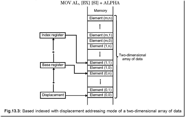
This addressing mode is used to access a two dimensional (m × n) array, as shown in Fig. 13.3. The displacement, having a fixed value, locates the starting position of the array in the memory while the base register specifies one coordinate (say m) and index register the other coordinate (say n). Any position in the array can be located simply by changing the values in the base and index registers.

An example of this mode of addressing is as follows:

Addressing Modes of 8086 5-20-35 PM

Thus the offset or effective address can be calculated from the contents of base and index registers and the fixed displacement as represented by ALPHA.

Assuming: DS = 3000 H, BX = 1000 H, SI = 1234 H and ALPHA (displacement) = 0012 H. Thus, PA = 03000 H + 1000 H + 1234 H + 0012 H = 05246 H.

On executing this instruction, the value stored in memory location 05246 H (source operand) will be stored in AL. Here, memory address is the sum of an index register, a base register and an 8 or 16-bit displacement within the instruction.


Memory Organisation

Memory Organisation

1. Mention the address capability of 8086 and also show its memory map.

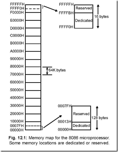
Ans. 8086, via its 20-bit address bus, can address 220 = 1,048,576 or 1 MB of different memory locations. Thus the memory space of 8086 can be thought of as consisting of 1,048,576 bytes or 524,288 words.

The memory map of 8086 is shown in Fig. 12.1, where the whole memory space starting from 00000 H to FFFFF H is divided into 16 blocks—each one consisting of 64 KB. This division is arbitrary but at the same time a convenient one—because the most significant hex digit increases by 1 with each additional block. Thus, 30000 H memory location is 65,536 bytes higher in memory than the memory location 20000 H.

Memory Organisation4-59-18 PM

The lower and upper ends of the memory map are shown separately—earmarking some spaces as reserved and some as ‘dedicated’.

The reserved locations are meant for future hardware and software needs while the dedicated locations are used for processing of specific system interrupts and reset functions.

2. Mention the different types of memory segmentations of 8086.

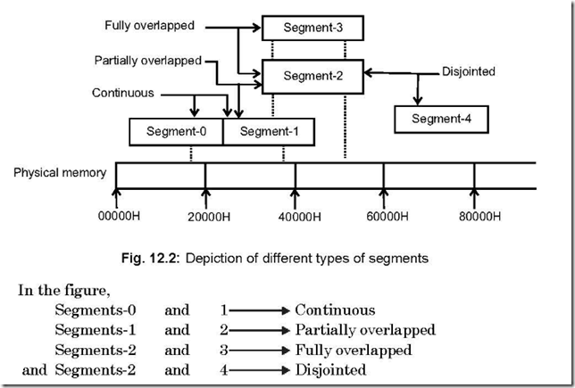
Ans. The different memory segmentations done in case of 8086 are

z Continuous

z partially overlapped

z fully overlapped and

z disjointed

This is shown in Fig.12.2.

Memory Organisation5-00-02 PM

3. Describe memory segmentation scheme of 8086. What is meant by currently active segments?

Ans. 1 MB memory of 8086 is partitioned into 16 segments—each segment is of 64 KB length.

Out of these 16 segments, only 4 segments can be active at any given instant of time— these are code segment, stack segment, data segment and extra segment. The four memory segments that the CPU works with at any time are called currently active segments. Corresponding to these four segments, the registers used are Code Segment Register (CS), Data Segment Register (DS), Stack Segment Register (SS) and Extra Segment Register (ES) respectively.
Each of these four registers is 16-bits wide and user accessible—i.e., their contents can be changed by software.

The code segment contains the instruction codes of a program, while data, variables and constants are held in data segment. The stack segment is used to store interrupt and subroutine return addresses.
The extra segment contains the destination of data for certain string instructions. Thus 64 KB are available for program storage (in CS) as well as for stack (in SS) while 128 KB of space can be utilised for data storage (in DS and ES).

One restriction on the base address (starting address) of a segment is that it must reside on a 16-byte address memory—examples being 00000 H, 00010 H or 00020 H, etc.

4. Mention the maximum size of memory that can be active for 8086. Ans. The maximum size of active memory for 8086 is 256 KB. The break-up being

64 KB for program

64 KB for stack and

128 MB for data.

5. Why memory segmentation is done for 8086?

Ans. Memory segmentation, as implemented for 8086, gives rise to the following advantages:

z Although the address bus is 20-bits in width, memory segmentation allows one to work with registers having width 16-bits only.

z It allows instruction code, data, stack and portion of program to be more than 64 KB

long by using more than one code, data, extra segment and stack segment.
z In a time-shared multitasking environment when the program moves over from one user’s program to another, the CPU will simply have to reload the four segment registers with the segment starting addresses assigned to the current user’s program.

z User’s program (code) and data can be stored separately.

z Because the logical address range is from 0000 H to FFFF H, the same can be loaded at any place in the memory.

6. Discuss logical address, base segment address and physical address.

Ans. The logical address, also goes by the name of effective address or offset address (also known as offset), is contained in the 16-bit IP, BP, SP, BX, SI or DI.

The 16-bit content of one of the four segment registers (CS, DS, ES, SS) is known as the base segment address.

Offset and base segment addresses are combined to form a 20-bit physical address (also called real address) that is used to access the memory. This 20-bit physical address is put on the address bus (AD19 – AD0) by the BIU.

7. Describe how the 20-bit physical address is generated.

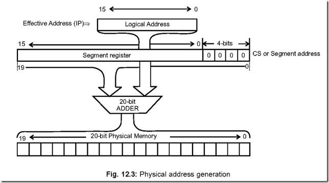
Ans. The 20-bit physical (real) address is generated by combining the offset (residing in IP, BP, SP, BX, SI or DI) and the content of one of the segment registers CS, DS, ES or SS. The process of combination is as follows:

The content of the segment register is internally appended with 0 H (0000 H) on its right most end to form a 20-bit memory address—this 20-bit address points to the start of the segment. The offset is then added to the above to get the physical address.
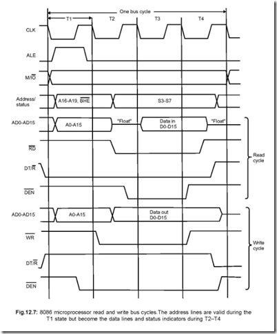
Fig. 12.3 shows pictorially the actual process of generating a 20-bit physical address.

Memory Organisation5-00-25 PM

Thus, Physical Address = Segment Register content 16 D + Offset.

8. Although 8086 is a 16-bit µP, it deals with 8-bit memory. Why?

Ans. This is so for the following two reasons:

z It enables the microprocessor to work with both on bytes and words. This is very important because many I/O devices such as printers, terminals, modems etc, transfer ASCII coded data (7 or 8 bits).

z Quite a few of the operation codes of 8086 are single bytes while so many other instructions are there which vary from 2 to 7 bytes. By working with byte-width memory, these varied opcodes can easily be handled.

9. Is the flat scheme of memory applied for 8086 µP?

Ans. No, the flat (or unsegmented) scheme of memory is not applied for 8086 µP, because the

memory of the same is a segmented one. In flat scheme, the entire memory space is

thought of as a single addressable memory unit.

The flat scheme can be applied for 8086 by initialising all the segment registers with identical (or same) base address. Then all memory operations will refer to the same memory space.

10. Describe how memory is organised for 8086 µP?

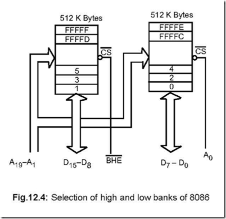
Ans. The total address space 1 MB of 8086 is divided into 2 banks of memory—each bank of maximum size 512 KB. One is called the high order memory bank (or high bank) and the other low order memory bank (or low bank).

Low bank, high bank or both banks can be accessed by utilizing two signals BHE

and A0. Table 12.1 shows the three possible references to memory.

Table 12.1: Memory references

BHE

A0

Processing

0

0

Both Banks Active 16-bit world transfer on AD15 ⇔ AD0

0

1

Only High bank Active (One byte from/to odd address on AD ⇔ AD )

15 8

1

0

Only Low bank Active (One byte from/to even address on AD ⇔ AD )

7 0

1

1

No Bank Active

The high bank is selected for A0=1 and BHE =0 and is connected to D15–D8 while the low bank is selected for A0=0 and BHE =1. Neither low bank nor high bank would selected

for A0=1 and BHE =1.

Fig. 12.4 shows how the total address space (1MB) of 8086 is physically implemented

by segregating it into low and high banks. It also shows that CS signal of the high bank is connected to BHE while the CS signal of the low bank is connected to A0.

Memory Organisation5-01-08 PM

11. Show the profiles of low and high order memory banks.

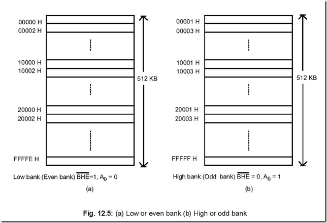
Ans. The low and high order memory banks correspond to even and odd banks respectively.

The CS signal of low order memory bank is selected when CS = 0. Since A0 (lowest address bus line) is connected to CS , hence A0 must have be to low for the low order bank

to be selected. That is why the low order bank corresponds to even bank. Similarly the

high order bank is selected when A0 = 1. Hence, the higher order bank is called odd bank.

The profile of the low and high order banks are shown below in Fig. 12.5

Memory Organisation5-01-27 PM

12. Draw the diagrams of (a) even-addressed byte transfer (b) odd-addressed byte transfer (c) even-addressed word transfer and (d) odd-addressed word transfer.

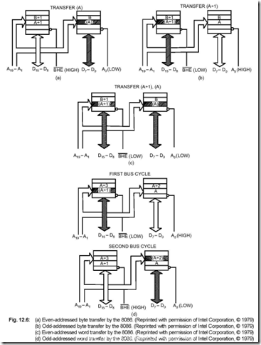
Ans. Fig. 12.6 shows the above four cases. A, B are representing the addresses while (A), (B) represent the content of address locations A and B respectively.

Figures (a) and (b) correspond to byte transfers for even and odd-addressed memory locations respectively. The shaded memory location indicates that the content of that particular memory location comes out either via higher byte data bus (D15–D8) or lower byte data bus (D7–D0) respectively.

Figures (a), (b) and (c) complete the data transfer in one bus cycle only.

For Figure (a), BHE = 1, A0 = 0

For Figure (b), BHE = 0, A0 = 1

For Figure (c), BHE = 0, A0 = 0

Figure (d) corresponds to an odd-addressed word transfer and it takes two bus cycles

to complete this transfer.

Memory Organisation5-02-06 PM

This odd-addressed word is an unaligned one and the LSB of the address is in the high memory bank.

The odd byte of the word is at address location A + 1 and is selected by making

clip_image041[5]BHE = 0 and A0. Thus in the first bus cycle, data to transferred on D15 – D8.

In the second bus cycle, 8086 automatically increments the address. Hence A0

becomes 0, representing even address A + 2. This is in the low bank and is accessed by

clip_image053[4]making BHE = 1 and A0 = 0.

13. Which pins identify the segment registers used for 20-bit physical address generation?

Ans. Pins A16 and A17 become S3 and S4 from the second bus cycle. This 2-bit combination of S3 and S4 indicate the segment register used for physical address generation and is shown in Table 12.2

Table 12.2: Identifying the segment register used for 20-bit physical address generation

S4

S3

Segment Register

0

0

Extra

0

1

Stack

1

0

Code/none

1

1

Data

The two status codes are output both in the maximum and minimum mode.

14. What is the maximum size of the memory that can be accessed by 8086?

Ans. The two status codes S4 and S3 together point to the segment register used for 20-bit physical address generation and can be examined by external circuitry to enable separate 1 MB address space for each of CS, ES, DS, and SS. This would enable memory address

to be expanded to a maximum of 4MB for 8086 µP.

15. Draw the Read and Write bus cycles for 8086 µP in Minimum mode.

Ans. Fig. 12.7 shows the Read and Write bus cycles for 8086 µP in the Minimum mode.

The bus cycle consists of 4T states. ALE signal stays high for T1 state at the end of which it goes low which is utilised by latches to latch the address. Hence, during

T2 – T4 states, AD15 – AD0 lines act as data lines. The M/ IO , RD and WR signals can be combined to generate individual IOR, IOW and MEMR, MEMW signals.

The Read and Write cycles show that data are made available during T3 and T2 states respectively.

Memory Organisation5-03-07 PM


The 8086 Microprocessor

The 8086 Microprocessor

1. Draw the pin diagram of 8086.

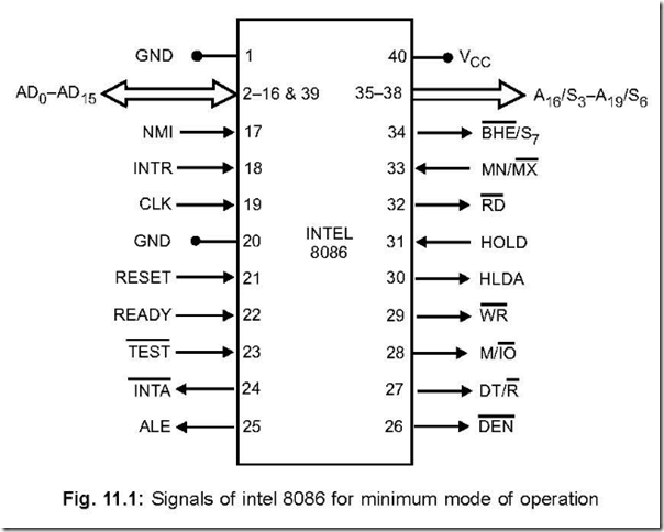
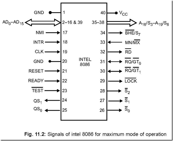
Ans. There would be two pin diagrams—one for MIN mode and the other for MAX mode of 8086, shown in Figs. 11.1 and 11.2 respectively. The pins that differ with each other in the two modes are from pin-24 to pin-31 (total 8 pins).

The 8086 Microprocessor 8-51-11 PM

2. What is the technology used in 8086 µP?

Ans. It is manufactured using high performance metal-oxide semiconductor (HMOS) technology. It has approximately 29,000 transistors and housed in a 40-pin DIP package.

3. Mention and explain the modes in which 8086 can operate. Ans. 8086 µP can operate in two modes—MIN mode and MAX mode.

When MN/MX pin is high, it operates in MIN mode and when low, 8086 operates in MAX mode.

For a small system in which only one 8086 microprocessor is employed as a CPU, the system operates in MIN mode (Uniprocessor). While if more than one 8086 operate in a system then it is said to operate in MAX mode (Multiprocessor).

The 8086 Microprocessor 8-52-14 PM

The bus controller IC (8288) generates the control signals in case of MAX mode, while in MIN mode CPU issues the control signals required by memory and I/O devices.

4. Distinguish between the lower sixteen address lines from the upper four.

Ans. Both the lower sixteen address lines (AD0 − AD15 ) and the upper four address lines

(A16 / S3 − A19 / S6 ) are multiplexed.

During T1, the lower sixteen lines carry address (A0 − A15 ) , while during T2, T3 and T4 they carry data.

Similarly during T1, the upper four lines carry address (A16– A19), while during T2,

T3 and T4 , they carry status signals.

5. In how many modes the minimum-mode signal can be divided?

Ans. In the MIN mode, the signals can be divided into the following basic groups: address/data bus, status, control, interrupt and DMA.

6. Tabulate the common signals, Minimum mode signals and Maximum mode signals. Also mention their functions and types.

Ans. Table 11.1 shows the common signals, Minimum mode signals and the Maximum mode signals, along with the functions of each and their types.

Table 11.1 : (a) Signals common to both minimum and maximum mode, (b) Unique minimum-mode signals, (c) Unique maximum-mode signals for 8086.

The 8086 Microprocessor 8-52-46 PM

7. Mention the different varieties of 8086 and their corresponding speeds.

Ans. The following shows the different varieties of 8086 available and their corresponding speeds.

Types          Speeds

8086 5         MHz

8086–1        10 MHz

8086–2          8 MHz

8. Mention (a) the address capability of 8086 and (b) how many I/O lines can be accessed by 8086.

Ans. 8086 addresses via its A0–A19 address lines. Hence it can address 220 = 1MB memory.

Address lines A0 to A15 are used for accessing I/O’s. Thus, 8086 can access 216 = 64

KB of I/O’s.

9. What is meant by microarchitecture of 8086?

Ans. The individual building blocks of 8086 that, as a whole, implement the software and hardware architecture of 8086. Because of incorporation of additional features being necessitated by higher performance, the microarchitecture of 8086 or for that matter any microprocessor family, evolves over time.

10. Draw and discuss the architecture of 8086. Mention the jobs performed by BIU and EU.

Ans. The architecture of 8086 is shown below in Fig. 11.3. It has got two separate functional units—Bus Interface Unit (BIU) and Execution Unit (EU).

8086 architecture employs parallel processing—i.e., both the units (BIU and EU) work at the same time. This is Unlike 8085 in which Sequential fetch and execute operations take place. Thus in case of 8086, efficient use of system bus takes place and higher performance (because of reduced instruction time) is ensured.

z BIU has segment registers, instruction pointer, address generation and bus control logic block, instruction queue while the EU has general purpose registers, ALU, control unit, instruction register, flag (or status) register.

The main jobs performed by BIU are:

z BIU is the 8086’s interface to the outside world, i.e., all External bus operations

are done by BIU.

z It does the job of instruction fetching, reading/writing of data/operands for memory

and also the inputting/outputting of data for peripheral devices.

z It does the job of filling the instruction queue.

z Does the job of address generation.

The main jobs performed by the execution unit are:

z Decoding/execution of instructions.

z It accepts instructions from the output end of instruction queue (residing in BIU)

and data from the general purpose registers or memory.

z It generates operand addresses when necessary, hands them over to BIU

requesting it (BIU) to perform read or write cycle to memory or I/O devices.

z EU tests the status of flags in the control register and updates them when

executing instructions.

z EU waits for instructions from the instruction queue, when it is empty.

z EU has no connection to the system buses.

The 8086 Microprocessor 8-53-52 PM

11. Explain the operations of instructions queue residing in BIU.

Ans. The instruction queue is 6-bytes in length, operates on FIFO basis, and receives the instruction codes from memory. BIU fetches the instructions meant for the queue ahead of time from memory. In case of JUMP and CALL instructions, the queue is dumped and newly formed from the new address.

Because of the instruction queue, there is an overlap between the instruction execution and instruction fetching. This feature of fetching the next instruction when the current instruction is being executed, is called Pipelining.

The 8086 Microprocessor 8-54-12 PM

Fig. 11.4, which is self-explanatory, shows that there is definitely a time saved in case of overlapping phases (as in the case of 8086) compared to sequential phases (as in the case of 8085). Initially, the queue is empty and CS : IP is loaded with the required address (from which the execution is to be started). Microprocessor 8086 starts operation by fetching

1 (or 2) byte(s) of instruction code(s) if CS : IP address is odd (even).

The 1st byte is always an opcode, which when decoded, one byte in the queue becomes empty and the queue is updated. The filling in operation of the queue is not started until two bytes of the instruction queue is empty. The instruction execution cycle is never broken for fetch operation.

After decoding of the 1st byte, the decoder circuit gets to know whether the instruction is of single or double opcode byte.

For a single opcode byte, the next bytes are treated as data bytes depending upon the decoded instruction length, otherwise the next byte is treated as the second byte of the instruction opcode.

The 8086 Microprocessor 8-54-32 PM

For a 2-byte instruction code, the decoding process takes place taking both the bytes into consideration which then decides on the decoded instruction length and the number of subsequent bytes which will be treated as instruction data. Updation of the queue takes place once a byte is read from the queue.

The queue operation is shown in Fig. 11.5 in block schematic form.

12. Mention the conditions for which EU enters into WAIT mode.

Ans. There are three conditions that cause the EU to enter into WAIT state. These are:

z When an instruction requires the access to a memory location not in the queue.

z When a JUMP instruction is executed. In this case the current queue contents are

aborted and the EU waits until the instructions at the jump address is fetched from

memory.

z During execution of instruction which are very slow to execute. The instruction AAM

(ASCII adjust for multiplication) requires 83 clock cycles for execution. For such a

case, the BIU is made to wait till EU pulls one or two bytes from the queue before

resuming the fetch cycle.

13. Mention the kind of operations possible with 8086.

Ans. It can perform bit, byte, word and block operations. Also multiplication and division operations can be performed by 8086.

14. Mention the total number of registers of 8086 and show the manner in which they are grouped.

Ans. There are in all fourteen numbers of 16-bit registers. The different groups are made as hereunder:

z Data group, pointers and index group, status and control flag group and segment group.

z The data group consists of AX (accumulator), BX (base), CX (count) and DX (data).

z Pointer and Index group consist of SP (Stack pointer), BP (Base pointer), SI (Source

Index), DI (Destination index) and IP (Instruction pointer).

z Segment group consists of ES (Extra Segment), CS (Code Segment), DS (Data

Segment) and SS (Stack Segment).

z Control flag group consists of a single 16-bit flag register.

Fig. 11.6 shows the registers placed in the different groups to form a programming

model.

The 8086 Microprocessor 8-54-54 PM

15. Describe, in detail, the general purpose of data registers.

Ans. Fig. 11.7 shows the four data registers along with their dedicated functions also.

All the four registers can be used bytewise or wordwise. The alphabets X, H and L respectively refer to word, higher byte or lower byte respectively of any register.

All the four registers can be used as the source or destination of an operand during an arithmetic operation such as ADD or logical operation such as AND, although particular registers are earmarked for specific operations. Register C is used as a count register in string operations and as such is called a ‘count’ register. Register C is also used for multibit shift or rotate instructions.

Register D is used to hold the address of I/O port while register A is used for all I/O operations that require data to be inputted or outputted.

16. Describe the status register of 8086.

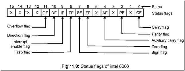
clip_image071_thumbAns. It is a 16-bit register, also called flag register or Program Status Word (PSW). Seven bits remain unused while the rest nine are used to indicate the conditions of flags. The status flags of the register are shown below in Fig. 11.8.

The 8086 Microprocessor 8-55-29 PM_thumb

Out of nine flags, six are condition flags and three are control flags. The control flags are TF (Trap), IF (Interrupt) and DF (Direction) flags, which can be set/reset by the programmer, while the condition flags [OF (Overflow), SF (Sign), ZF (Zero), AF (Auxiliary Carry), PF (Parity) and CF (Carry)] are set/reset depending on the results of some arithmetic or logical operations during program execution.

CF is set if there is a carry out of the MSB position resulting from an addition

operation or if a borrow is needed out of the MSB position during subtraction.

PF is set if the lower 8-bits of the result of an operation contains an even number of 1’s. AF is set if there is a carry out of bit 3 resulting from an addition operation or a borrow required from bit 4 into bit 3 during subtraction operation.

ZF is set if the result of an arithmetic or logical operation is zero.

SF is set if the MSB of the result of an operation is 1. SF is used with unsigned

numbers.

OF is used only for signed arithmetic operation and is set if the result is too large to be fitted in the number of bits available to accommodate it.

The functions of the flags along with their bit positions are shown in Fig. 11.9 below.

The 8086 Microprocessor 8-55-51 PM_thumb

The 8086 Microprocessor 8-56-12 PM_thumb[1]

17. Discuss the three control flags of 8086.

Ans. The three control flags of 8086 are TF, IF and DF. These three flags are programmable, i.e., can be set/reset by the programmer so as to control the operation of the processor.

When TF (trap flag) is set (=1), the processor operates in single stepping mode—i.e.,

pausing after each instruction is executed. This mode is very useful during program development or program debugging.

When an interrupt is recognised, TF flag is cleared. When the CPU returns to the

main program from ISS (interrupt service subroutine), by execution of IRET in the last line of ISS, TF flag is restored to its value that it had before interruption.

TF cannot be directly set or reset. So indirectly it is done by pushing the flag register

on the stack, changing TF as desired and then popping the flag register from the stack.

When IF (interrupt flag) is set, the maskable interrupt INTR is enabled otherwise

disabled (i.e., when IF = 0).

IF can be set by executing STI instruction and cleared by CLI instruction. Like TF flag, when an interrupt is recognised, IF flag is cleared, so that INTR is disabled. In the last line of ISS when IRET is encountered, IF is restored to its original value.

When 8086 is reset, IF is cleared, i.e., resetted.

DF (direction flag) is used in string (also known as block move) operations. It can be

set by STD instruction and cleared by CLD. If DF is set to 1 and MOVS instruction is

executed, the contents of the index registers DI and SI are automatically decremented to access the string from the highest memory location down to the lowest memory location.

18. Discuss the Pointers and Index group of registers.

Ans. The pointer registers are SP and BP while the index registers are SI and DI.

All the four are 16-bit registers and are used to store offset addresses of memory

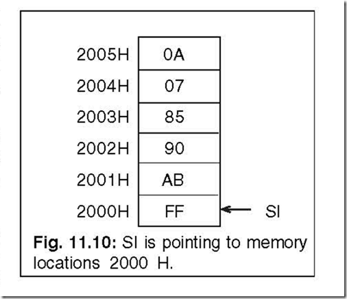
locations relative to segment registers. They act as memory pointers. As an example, MOV AH, [SI] implies, “Move the byte whose address is contained in SI into AH”. If now, SI = 2000 H, then execution of above instruction will put the value FF H in register AH, shown in Fig. 11.10, [SI+1 : SI] = ABFF H, where obviously SI+1 points to memory location 2001 H and [SI+1] = AB H.

SI and DI are also used as general purpose registers. Again in certain string (block

move) instructions, SI and DI are used as source and destination index registers

respectively. For such cases, contents of SI are added to contents of DS register to get the actual source address of data, while the contents of DI are added to the contents of ES to get the actual destination address of data.

SP and BP stand for stack pointer and base pointer with SP containing the offset address or the stack top address. The actual stack address is computed by adding the contents of SP and SS.

Data area(s) may exist in stack. To access such data area in stack segment, BP register is used which contains the offset address. BP register is also used as a general purpose register.

The 8086 Microprocessor 8-56-39 PM_thumb

Instruction pointer (IP) is also included in the index and pointers group. IP points to the offset instead of the actual address of the next instruction to be fetched (from the current code segment) in BIU. IP resides in BIU but cannot be programmed by the programmer.

19. Describe in brief the four segment registers.

Ans. The four segment registers are CS, DS, ES and SS—standing for code segment register, data segment register, extra segment register and stack segment register respectively. When a particular memory is being read or written into, the corresponding memory address is determined by the content of one of these four segment registers in conjunction with their offset addresses.

The contents of these registers can be changed so that the program may jump from one active code segment to another one.

The use of these segment registers will be more apparent in memory segmentation schemes.

20. Discuss A16/S3A19/S6 Signals of 8086.

Ans. These are time multiplexed signals. During T1, they represent A19 – A16 address lines.

During I/O operations, these lines remain low. During T2–T4, they carry status signals.

S4 and S3 (during T2 to T4) identify the segment register employed for 20-bit physical

address generation.

Status signal S5 (during T2 to T4) represents interrupt enable status. This is updated at the beginning of each clock cycle.

Status signal S6 remains low during T2to T4 .

21. Discuss BHE/S7 signal.

Ans. During T1, this becomes bus high enable signal and remains low while during T2 to T4 it acts as a status signal S7 and remains high during this time.

During T1, when BHE signal is active, i.e., remains low, it is used as a chip select signal on the higher byte of data bus—i.e., D15–D8.

Table 11.2 shows BHE and A0 signals determine one of the three possible references to memory.

The 8086 Microprocessor 8-57-20 PM_thumb[1]

22. Discuss the Reset pin of 8086.

Ans. Reset is an active high input signal and must be active for at least 4 CLK cycles to be accepted by 8086. This signal is internally synchronised and execution starts only after Reset returns to low value.

For proper initialisation, Reset pulse must not be applied before 50µS of ‘power on’

of the circuit. During Reset state, all three buses are tristated and ALE and HLDA are driven low.

During resetting, all internal register contents are set to 0000 H, but CS is set to F000 H and IP to FFF0 H. Thus execution starts from physical address FFFF0 H. Thus EPROM in 8086 is interfaced so as to have the physical memory location forms FFFF0 H to FFFFF H, i.e., at the end of the map.

23. Discuss the two pins (a) DT/ R and (b) DEN .

Ans. (a) DT/ R is an output pin which decides the directions of data flow through the transreceivers (bidirectional buffers).

When the processor sends out data, this signal is 1 while when it receives data,

the signal status is 0.

(b) DEN stands for data enable. It is an active low signal and indicates the availability of data over the address/data lines. This signal enables the transreceivers to separate data from the multiplexed address/data signal. It is active from the middle of T2 until

the middle of T4.

Both DT/ R and DEN are tristated during ‘hold acknowledge’.

24. Elaborate the functions of the pins S2 , S1 and S0 .

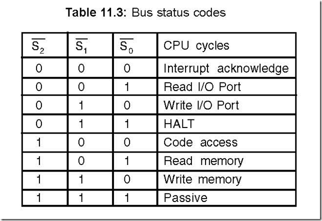
Ans. These three are output status signals in the MAX mode, indicating the type of operation carried out by the processor.

The signals become active during T4 of the previous cycle and remain active during T1 and T2 of the current cycle. They return to the passive state during T3 of the current bus cycle so that they may again become active for the next bus cycle during T4. Table

11.3 shows the different bus cycles of 8086 for different combinations of these three

signals.

The 8086 Microprocessor 8-57-41 PM_thumb

25.Explain the LOCK signal.

Ans. It is an active low output signal and is activated by LOCK prefix instruction and remains active until the completion of the next instruction. It floats to tri-state during hold

clip_image087_thumbacknowledge when LOCK signal is low, all interrupts get masked and HOLD request is not granted. LOCK signal is used by the processor to prevent other devices from

accessing the system control bus. This symbol is used when CPU is executing some critical instructions and through this signal other devices are informed that they should not issue HOLD signal to 8086.

26. clip_image089_thumbExplain the TEST signal.

clip_image090_thumbAns. It is an active low input signal. Normally the BUSY pin (output) of 8087 NDP is connected to the TEST input pin of 8086. When maths co-processor 8087 is busy executing some

clip_image091_thumbinstructions, it pulls its BUSY signal high. Thus the TEST signal of 8086 is consequently high, and it (8086) is made to WAIT until the BUSY signal goes low. When 8087

clip_image092_thumbcompletes its instruction executions, BUSY signal becomes low. Thus the TEST input of 8086 becomes low also and then only 8086 goes in for execution of its program.

27. Show how demultiplexing of address/data bus is done and also show the availability of address/data during read/write cycles.

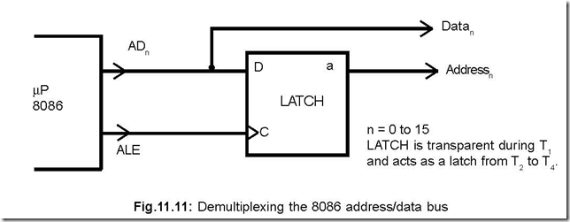
Ans. The demultiplexing of lower 2-bytes of address/data bus (AD0–AD15) is done by 8282/8283 octal latch with 8282 providing non-inverting outputs while 8283 gives out inverted outputs. The chip outputs are also buffered so that more drive is available at their outputs.

A D latch is central to the demultiplexing operations of these latches. During T1 when ALE is high, the latch is transparent and the output of latch is ‘A’ (address) only. At the end of T1, ALE has a high to low transition which latches the address available at the D input of the latch, so that address is continued to be available from the Q output of the latch (i.e., whole of T1 to T4 states).

It is to be noted that memory and I/O devices do not access the data bus until the

beginning of T2, thus the ‘data’ is a ‘don’t care’ till the end of T1. This is shown in Fig. 11.11 and the timing diagram shows the availability of data for read and write cycles.

The 8086 Microprocessor 8-58-06 PM_thumb

28. Discuss the Instruction Pointer (IP) of 8086.

Ans. Functionally, IP plays the part of Program Counter (PC) in 8085. But the difference is that IP holds the offset of the next word of the instruction code instead of the actual address (as in PC).

IP along with CS (code segment) register content provide the 20-bit physical (or real) address needed to access the memory. Thus CS:IP denotes the value of the memory address of the next code (to be fetched from memory).

Content of IP gets incremented by 2 because each time a word of code is fetched from memory.

29. Indicate the data types that can be handled by 8086 µP.

Ans. The types of data formats that can be handled by 8086 fall under the following categories:

z Unsigned or signed integer numbers—both byte-wide and word-wide.

z BCD numbers—both in packed or unpacked form.

z ASCII coded data. ASCII numbers are stored one number per byte.

30. Compare 8086 and 8088 microprocessors.

Ans. The Comparison between the two is tabulated below in Table 11.4.

8086

8088

1. 2-byte data width, obtained by demultiplexing AD –AD .

2. In MIN mode, pin-28 is assigned the signal M/ IO.

3. A 6-byte instruction queue.

4. To access higher byte, BHE signal is used.

5. BIU dissimilar, but EU similar to 8088. Program instructions identical to 8088.

6. Program fetching from memory done only when 2-bytes are empty in queue.

7. Pin-34 is BHE /S7. During T1, BHE is used to enable data on D –D . During T –T , status of this pin is 0. In MAX mode, 8087 monitors this pin

to identify the CPU—8086 or 8088? Accordingly it sets its queue length to 6 or 4 respectively.

1. 1-byte data width, obtained by demultiplexing AD –AD .

2. In MIN mode, pin-28 is assigned the signal IO/ M .

3. A 4-byte instruction queue.

4. No such signal required, since data width is 1-byte only.

5. BIU dissimilar, but EU similar to 8086. Program instructions identical to 8086.

6. Program fetching from memory done as soon as a byte is free in queue.

7. Pin-34 is SS0 . It acts as S0 in the MIN mode. In MAX mode SS0 = 1 always.

31. Comment on the instruction size of 8086. Ans. It varies from 1 to 6 bytes.

32. Discuss the instruction format of 8086.

Ans. The instruction format of 8086 is shown in Fig. 11.12. It is extendable up to 6-bytes. The first byte contains D and W—Direction Register Bit and Data Size Bit respectively. Both D and W are 1-bit in nature.

The 8086 Microprocessor 8-58-46 PM_thumb

z If D = 1, then register operand existing in byte-2 is the destination operand, otherwise (i.e., if D = 0) it is a source operand.

z W indicates whether the operation is an 8-bit or a 16-bit data. If W = 0 then it is an

8-bit operation, else (i.e., W = 1) it is 16-bit one.

z The 2nd byte (byte-2) indicates whether one of the operands is in memory or both are in registers. This byte contains three fields:

Field

Abbreviation

Length (no. of bits)

Mode field

MOD

2

Register field

REG

3

Register/Memory field

r/m

3

33. Discuss the MOD and r/m and REG fields.

Ans. MOD field is a 2-bit field. It addresses memory in the following manner.

MOD field values

0 0 ====>Memory addressing without displacement

0 1 ====>Memory addressing with 8-bit displacement

1 0====> Memory addressing with 16-bit displacement

1 1 ====>Register addressing with

W = 0 for 8-bit data

and W = 1 for 16-bit data

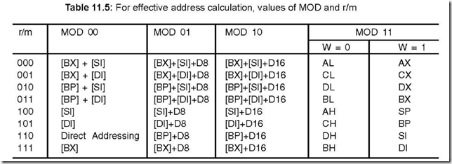
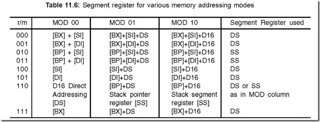
The r/m field which is a 3-bit field, along with MOD field defines the 2nd operand. If MOD = 11, then it is a register to register mode. Again if MOD = 00,01 or 10 then it is a memory mode. Table 11.5 shows how effective address of memory operand gets selected for MOD = 00,01 and 10 values.The 8086 Microprocessor 8-59-25 PM_thumb

Again, for MOD values 00,01 and 10, the default segment registers selected are shown in Table 11.6.

The 8086 Microprocessor 8-59-56 PM_thumb

The REG field is a 3-bit field and indicates the register for the first operand which can be source/destination operand, depending on D = 0/1.

How REG field along with the status of W(0 or 1) select the different registers, is shown in Table 11.7.

34. Discuss the instruction format for segment override prefix.

Ans. Default segment selection can be overriden by the override prefix byte, as shown in below.

The 8086 Microprocessor 9-00-29 PM_thumb[1]

Depending on the 2-bit rr values, the segments selected are shown in Table 11.8.

The 8086 Microprocessor 9-00-47 PM_thumb

The override prefix byte follows the opcode byte of the instruction, whenever used.

35. Is direct memory to memory data transfer possible in 8086?

Ans. No, 8086 does not have provision for direct memory to memory data transfer. For this to be implemented, AX is used as an intermediate stage of data. The source byte (from the memory) is moved into AX register with one instruction. The second instruction moves the content of AX into destination location (into another memory location). As example,

MOV AH, [SI]

MOV [DI], AH

Here, the first instruction moves the content of memory location, whose offset

address remains in SI, into AH. The second instruction ensures that the content of AH

is moved into another memory location whose offset address is in DI.

36. Can the data segment (DS) register be loaded directly by its address?

Ans. No, it cannot be done directly. Instead, AX is loaded with the initial address of the DS register and then it is transferred to DS register, as shown below:

MOV AX, DS ADDR: AX is loaded with initial address of DS register

MOV DS, AX: DS is loaded with AX, i.e., ultimately with DS ADDR

37. Show, in tabular form, the default and alternate segment registers for different types of memory references.

Ans. Table 11.9 shows the default and alternate register segments which can be used for different types of memory references.

The 8086 Microprocessor 9-01-10 PM_thumb[1]


USART 8251 (Universal Synchronous/ Asynchronous Receiver Transmitter)

USART 8251 (Universal Synchronous/ Asynchronous Receiver Transmitter)

1. Draw the pin diagram of USART 8251.

Ans. The pin diagram of 8251 is as shown below:

USART 8251 Universal Synchronous- Asynchronous Receiver Transmitter 6-46-39 PM

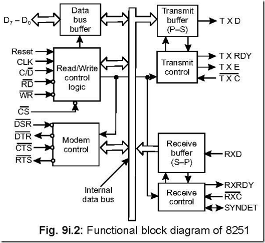
2. Draw the functional block diagram of 8251.

Ans. The functional block diagram of 8251 is shown below:

USART 8251 Universal Synchronous- Asynchronous Receiver Transmitter 6-47-22 PM

3. How many different sections does 8251 have?

Ans. 8251 has five sections: Read/Write control logic, data bus buffer, modem control, transmitter (including its control) and receiver (including its control).

4. How the 8251 is programmed?

Ans. 8251 is programmed by a 16-bit Control Word Register. This 16-bit register is divided into two bytes—the first byte corresponds to Mode Instruction Format while the second byte corresponds to Command Instruction Format. The content of control word register determines synchronous or asynchronous operation, Baud rate, number of bits per character, number of stop bits, nature of parity, etc.

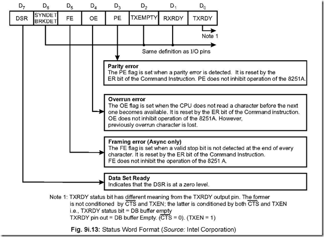
5. What is the function of the Status Word Register of 8251?

Ans. The function of the status word register is to check or examine the preparedness of 8251 with regard to transmission or reception of data.

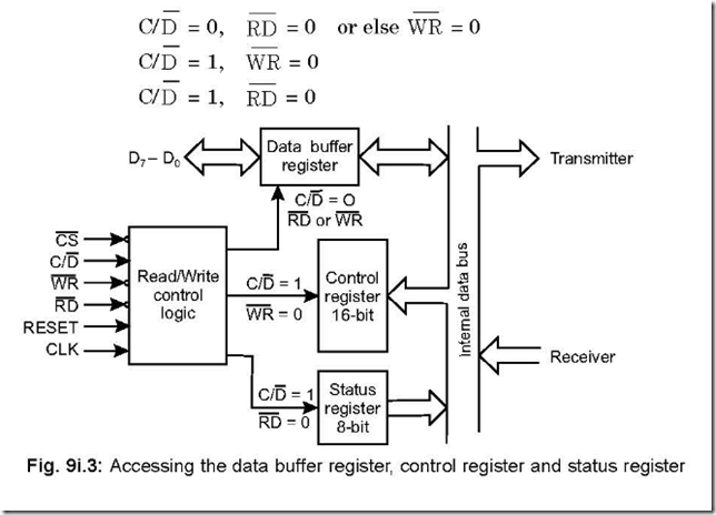
6. Describe the Read/Write Control logic and registers. Ans. It contains three buffer registers:

z data buffer register

z control register

z status register.

The six input signals are: CS , C/ D , WR, RD , RESET and CLK.

The particular 8251 is selected on CS signal going low. This pin is usually connected to a decoded address bus. C/ D stands for control/data pin. When this pin is high, either the control register or status register is selected and when low, data bus buffer is selected.

The control register and the status register are distinguished by WR and RD signals,

respectively.

The figure below shows how the three registers: data buffer register, control register

and status register are accessed by making respectively.

USART 8251 Universal Synchronous- Asynchronous Receiver Transmitter 6-48-45 PM

The following table shows the status of the control signals CS , C/ D , RD , WR for

accessing the different registers.

USART 8251 Universal Synchronous- Asynchronous Receiver Transmitter 7-15-17 PM

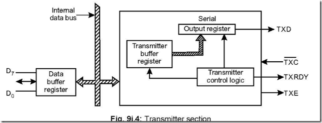
7.Explain the operation of the transmitter section of 8251.

Ans.

USART 8251 Universal Synchronous- Asynchronous Receiver Transmitter 7-15-38 PM

The transmitter section consists of three blocks—transmitter buffer register, output register and the transmitter control logic block. The CPU deposits (when TXRDY = 1, meaning that the transmitter buffer register is empty) data into the transmitter buffer register, which is subsequently put into the output register (when TXE = 1, meaning that the output buffer is empty). In the output register, the eight bit data is converted into serial form and comes out via TXD pin. The serial data bits are preceded by START bit and succeeded by STOP bit, which are known as framing bits. But this happens only if

clip_image015clip_image016transmitter is enabled and the CTS is low. TXC signal is the transmitter clock signal which controls the bit rate on the TXD line (output line). This clock frequency can be 1, 16 or 64 times the baud.

8. Explain the operation of the receiver section of 8251.

Ans.

USART 8251 Universal Synchronous- Asynchronous Receiver Transmitter 7-16-02 PM

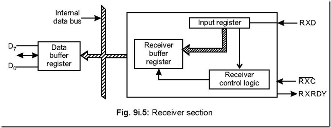
The receiver section consists of three blocks — receiver buffer register, input register and the receiver control logic block. Serial data from outside world is delivered to the input register via RXD line, which is subsequently put into parallel form and placed in the receiver buffer register. When this register is full, the RXRDY (receiver ready) line becomes high. This line is then used either to interrupt the MPU or to indicate its own status. MPU then accepts the data from the register.

clip_image016[1]RXC line stands for receiver clock. This clock signal controls the rate at which bits are received by the input register. The clock can be set to 1, 16 or 64 times the baud in the asynchronous mode.

9. How does the CPU know that the transmitter buffer is empty?

Ans. The CPU knows about the same by

z examining the TXRDY line of the transmitter.

z examining D0 bit of the status word.

10. When the TxD line goes into the MARKING (HIGH) state? Ans. It becomes high in the following cases:

z a RESET is received by 8251.

z transmitter is empty.

z transmitter is not enabled.

z CTS is off.

11. How the transmitter is enabled?

Ans. The transmitter is enabled by setting bit D0 of the command instruction word.

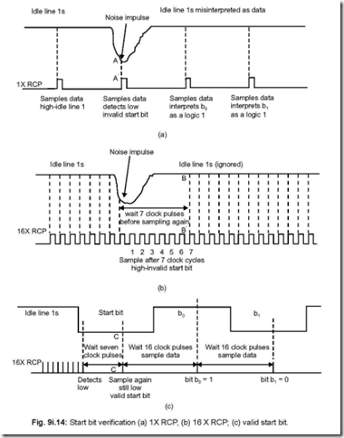
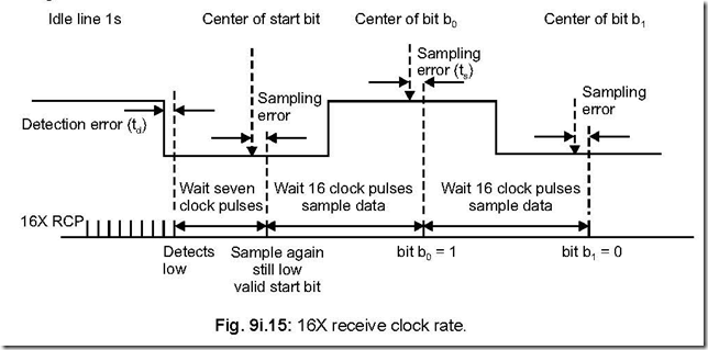
12. What is the status of the start bit on the RXD line for 8251 (in asynchronous mode only) and how does it differentiate between a valid start pulse and transient pulse?

Ans. For any data to be received by the receiver, it first checks for a valid start bit which is zero. 8251 has an inbuilt false start bit detection circuit which can differentiate between an actual start bit pulse and a transient pulse.

13. What happens when a parity error or a framing error occurs in the received data bits (in asynchronous mode only)?

Ans. The Parity error and Framing error status bits in the status word are set if there is a parity error or if the stop bit is absent at the end of the received bits respectively.

14. When the RXRdy line goes high in asynchronous and synchronous mode of operation?

Ans. In the asynchronous mode, RXRdy line goes high

z if the receiver is in the enabled condition (this is made so by setting D2 bit of the Command Instruction Word).

z and after the receiver has detected a valid start bit, assembled the character bits and transferred the character to the receiver buffer register.

Whereas in the synchronous mode RXRdy line goes high

z if the receiver is enabled.

z a character is assembled and transferred to the receiver buffer register.

15. What is overrun error?

Ans. D4 bit of the status word stands for ‘over run error’.

If the CPU cannot read the data from the receiver buffer register (this happens if the

CPU fails to respond to RXRdy line), then on receipt of the next character, the previous data will be written over and the earlier character will be lost. When such is the case D4 bit of the status word is set.

16. Discuss the SYNDET/BD pin.

Ans. This is pin 16 of 8251 and stands for sync. detect (SYNDET)/Break Detect (BRKDET).

This pin is used for detection of SYNC characters in synchronous mode and Break characters in asynchronous mode.

Synchronous mode: In the synchronous case this pin (SYNDET) can be used as either input or output pin with the help of control word. When the system is RESET, the status of this pin is low in the output mode. When 8251 is programmed to receive two synchronous characters, this output pin goes high at the mid point of the last bit of the second synchronous character. The status of this pin can also be known by reading the status word, but gets resetted on STATUS READ.

In the input mode—called the external synchronous detect mode—a rising edge on this pin causes 8251 to start collecting data characters on the rising edge of the next RXC . This input signal can be removed once synchronisation is achieved. When external synchronisation is done, the internal synchronisation is disabled.

BRKDET: In this mode, this pin acts as an output pin to detect break characters. If RXD remains low for two consecutive stop bit sequences, this pin (BRKDET) goes high. Here also provision is there to read the status of this pin by STATUS READ operation.

This pin is reset

z on a Master Chip Reset

z when RXD becomes on 1.

17. What purpose does 8251 serve—DTE or DCE in a communication interface environment?

Ans. 8251 acts as a DTE (Data Terminal Equipment) in such a case.

18. Why modems (modulators-demodulators) are used in case of digital transmission of data?

Ans. The term ‘modem’ stands for modulator—demodulator. In a communication environment, two modems are used—one at the transmitting end side and one at the receiving end side. Modems are generally called DCE (Data Communication Equipment).

High frequency digital signals require a very wide transmission channel bandwidth which makes the system very costly. However, existing telephone line facilities (which carry analog signals in the range of 40 Hz to 4 KHz) can be used to transmit such high frequency digital signals. A modem converts a digital signal into audio tone frequencies (at the transmitting end side) and reconverts this audio frequencies into h.f. digital signals (at the receiving end side)—and it utilises Frequency Shift Keying (FSK) for this purpose. Thus a modem converts a logical ‘1’ to 1200 Hz and ‘0’ to 2200 Hz audio frequency. These signals are then transmitted over a telephone line over a ‘carrier’. The inverse operation is done at the receiving end side.

158 Understanding 808518086 Microprocessors and Peripheral /Cs through Questions and Answers

19. Draw the block diagram of a DTE-DCE interface in a communication environment.
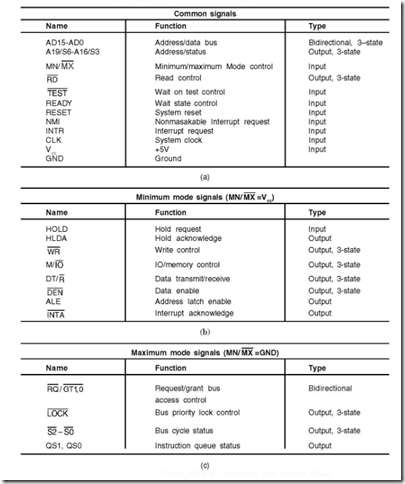
Ans. The block diagram is shown below:

USART 8251 Universal Synchronous- Asynchronous Receiver Transmitter 7-16-33 PM

Digital data is delivered at the DTE (may be 8251) in parallel form, which is then converted into serial form and sent to DCE via RS-232 cable. The DCE (a modem) output is an audio signal carried through a telephone line.

At the receiving end side, the opposite process is carried out to retrieve the original data.

20. Draw the 8251 data loading sequence and explain the same.

Ans. The data loading sequence of 8251 is shown below:

USART 8251 Universal Synchronous- Asynchronous Receiver Transmitter 7-17-34 PM

The mode control is specified first, which indicates the general operating conditions. If the mode word indicates that it is a synchronous operation, then the synchronous character(s) is/are loaded. This is followed by loading the command instruction format.

In all these, C/ D = 1. After this, C/ D is made 0 when data is either transmitted/received.

It is followed by command instruction and data in that order which is repeated all over again.

A command word with D6 = 1returns 8251 to mode instruction format.

21. Discuss the mode instruction format for asynchronous transmission/reception case.

Ans. The mode instruction format for asynch ronous (transmission/reception) is shown below:

Bits D0D 1 cannot both be low for asynchronous communication. These two bits determine the baud rate factor. Bits D2 D3 determine the character length (which may be 5 to 8 bits in length)-depending on the content of the se two bits. Bit D4 stands for ‘Parity Enable’ (PEN) and is enabled if D 1 = 1 and otwrwise if D1 = 0. D:, bit stands for ‘Even Parity’ (EPl. Parity is even if D;; = 1 and odd il D,, = 0. Bits D6 and D7 determine

the number of stop bits. There can be 1, 1 y . 2 numb•’r of stop bits.

USART 8251 Universal Synchronous- Asynchronous Receiver Transmitter 7-18-17 PM

22. Draw the general transmission/receive format for asynchronous communication. Ans. The general transmission/receive format for asynchronous communication is shown below: The transmission format consists of start bit, data character, parity bit, stop bit(s)­

in that order.

8251 starts sending data on the TXD (transmit data pin) pin with a start bit which is a 1to 0 transmission. Then the data bits are transmitted, followed by stop bit(s). The data bits start with LSB of the serial output register. All these bits (start bit, data bits,

stop bit(s) are shifted out on the falling edge of TXC (transmitter clock). In case when no data is transmitted, TXD output remains high. But if a ‘break’ is programmed, TXD line will go low.

USART 8251 Universal Synchronous- Asynchronous Receiver Transmitter 7-18-47 PM

The receive format is identical to transmit format. Data reception starts with RXD (receive data pin) line going low—it indicates the arrival of start bit. This 1 to 0 transition on the RXD line triggers the ‘False Start Bit Detection Circuit’. This circuit then samples the RXD line half-a-bit time later to ensure the presence of a genuine start bit. If this sampling results in a low on RXD line, it indicates a valid start bit. The bit counter is started on the second sampling—hence each subsequent data bit is

sampled at the middle of each bit period. This is called ‘mid bit sampling’. The bit counter thus samples the data bits, parity bit and lastly the stop bit. The receiver needs only one stop bit—but the transmitter is affected by the number of stop bits. For any error during receiving of data with regard to Parity, Framing or Overrun—the corresponding flags in the status word are set.

23. Why the ‘false start bit detection circuit’ is there in asynchronous reception case?

Ans. This is done to avoid any possibility of a false start bit detection due to a transient noise pulse.

24. Discuss the mode instruction format for synchronous transmission/reception case.

Ans. The mode instruction format for synchronous operation (transmission/reception) is shown below:

Bits D0 D1 both will have to be low for synchronous transmission/reception of data. Bits D2 D3 indicates the character length. Bits D4 and D5 stand for PEN and EP respectively—exactly same as in the case of asynchronous case. Bit D6 stands for ESD (External Synchronous Detect). D6 = 1 stands for input and D6 = 0 stands for output. Bit D7 stands for SCS (Single Character Sync.) with D7 = 1 indicating a single synchronous character and D7 = 0 indicating double synchronous characters.

USART 8251 Universal Synchronous- Asynchronous Receiver Transmitter 7-19-09 PM

25. Draw the general transmission/receive format for synchronous communication. Ans. The general transmission/receive format for synchronous communication is shown below.

USART 8251 Universal Synchronous- Asynchronous Receiver Transmitter 7-20-00 PM

clip_image042In the transmission format, either one or two synchronous characters are sent, followed by data characters. The number of synchronous characters (i.e., 1 or 2) is previously decided by the bit D6 in the mode instruction format for synchronous operation. For such communication to take place, C/ D will have to be 1. The characters are shifted out of the serial output register on the falling edge of the TXC (transmitter clock), and at the same rate as the TX C . Once transmission commences, it is the duty of the CPU to replenish the transmitter buffer register in response to TXRdy. If the CPU fails to provide a character before the transmitter buffer becomes empty, 8251 automatically sends SYNC character(s). In such a case, TXE (Transmitter Empty) pin becomes high to indicate that the transmitter buffer is empty.

In the receive format, C/ D is maintained at high level. In the internal SYNC mode, the receiver samples the data available as the RXD pin on the rising edge of RX C . The command word should be previously programmed with the ‘ENTER HUNT’ command (bit D7 of the Command Instruction Format) in the Enabled Condition (D7 = 1). The receiver buffer register content is compared at every bit boundary with the SYNC character (previously loaded) till a match occurs. The process is extended to two SYNC characters if the 8251 is initially programmed for two SYNC characters (bit D7 of the Mode Instruction Format). After ‘HUNTING’ is over, the system goes for character boundary synchronisation so that it can assemble the serial data to be subsequently changed to parallel format. The SYNDET pin is set high, which can be ascertained with a status read. This is resetted once status read is over. The SYNDET pin gets set in the middle of the parity bit if the parity is enabled; otherwise in the middle of the last data bit. In the external SYNC mode, 8251 comes out of HUNT mode by a high level on the SYNDET pin, which acts as an input in such a case.

26. Show the Command Instruction Format and explain the same. Ans. The Command Instruction Format is shown below:

USART 8251 Universal Synchronous- Asynchronous Receiver Transmitter 7-20-56 PM

The command instruction format controls the functioning of 8251. A command word with D6 = 1 returns 8251 in mode instruction format. If D0 (TXEN) is mode high, data transmission is possible whereas making D2 (RXE) high, enables the system for reception. If D1 (DTR) is made high, the DTR output will be forced in the zero state. A high on D4 (ER) forces resetting of error flags PE, OE and FE (Parity, overrun and Framing errors respectively) in the status word. A high on D3 (SBRK) forces TXD low while a zero corresponds to normal operation.

27. What happens when (a) power is switched on (b) the system is resetted?

Ans. On powering on the system, 8251 either enters into SYNC or command instruction format.

On resetting the system, 8251 returns to the mode instruction format from the command instruction format.

28. Draw the status word format and explain the same.

Ans. The status word format for 8251 is shown below

USART 8251 Universal Synchronous- Asynchronous Receiver Transmitter 7-22-02 PM

The status word can be read with C/ D = 1. The CPU, for its proper operation, needs various informations. These are provided by the status word. It should be borne in mind that the status word is continuously updated by 8251, but not while the CPU reads it.

29. What are the modem control pins associated with 8251? Describe the functioning of these pins.

Ans. The modem control section of 8251 are handled by these four pins: DSR , DTR , CTS and RTS . Out of these, the first and third are input pins (input to 8251) and the rest two are output pins. All these pins are active low. The signals on these pins are also used for purposes other than modem control. The description of these pins are given below:

DSR (Data Set Ready): This is a 1-bit inverting input port. It is used by the modem to signal the 8251 (here DTE) that it (modem) is ready to accept data for transmission. The DSR bit is checked by reading (polling) the D7 bit of the status word. If it is low, then the modem can send data to 8251.

DT R (Data Terminal Ready): This is a 1-bit inverting output port. It is used by 8251 to signal the modem about its readiness to accept/transmit data. D1 bit of command instruction word can either be set/reset, with a high D1 bit forcing DTR output to zero.

RTS (Request to Send): This is a 1-bit inverting output port. It is used by 8251 to signal the modem that it has data to send. Bit D5 of the Command Instruction Format controls the status of this pin.

CTS (Clear to Send): This is a 1-bit inverting input port. It is used by modem to signal 8251 that it has the right of way over the communication channel and can send out serial data. Bit D0 of the command instruction word should be enabled for the above to be realised.

If D0 is made low in command instruction word while data transmission is taking place or if CTS is switched off, the transmitter will complete sending the data stored in its buffer prior to getting disabled.

30. What is the baud rate of 8251?

Ans. The asynchronous baud rate of 8251 is 9600, while for the improved version of 8251— i.e., 8251A, this is 19, 200.

31. Discuss how a noise pulse may be recognised as a valid start pulse. How this possibility is eliminated?

Ans. In the asynchronous case, a USART may be programmed for receive clock rates of 8,16,32,64 times the receive data rate (these correspond to 8X, 16X, 32X and 64X). Thus the receive clock rates may be 8X RCP, 16X RCP, 32X RCP and 64X RCP, apart from the normal 1X RCP. Actually, 1X RCP corresponds to the receive data rate.

Fig. 9i.14(a) shows the situations when the line is idle (i.e., in state ‘1’) and is hit by

a noise impulse. The receive clock pulse (RCP) is set at 1X RCP. The figure shows the uneventful situation of the clock pulse sampling the input line at the instant the noise is present (point A A′ ) and the circuit detects a low. This gives rise to an invalid start bit and the subsequent clocks will interprete the high condition on the data line to be data bits—all at logic 1’s. This gives rise to a serious error arising out of an accidental noise pulse.

Fig. 9i.14(b) shows the same situation with the exception that the receiver clock is now made sixteen times faster—i.e., 16X RCP. Once a low is detected, the receiver is made to wait for seven clock cycles before it resamples the input data (this corresponds to BB′ in the fig.). Since in this case the receiver analyses the input line status to be ‘1’, hence it concludes that the low input line status that it detected seven clock cycles earlier to be a noise pulse. Thus the possibility of the UART receiver accepting spurious noise pulse is eliminated. This can further be improved by increasing the clock rate to 32X, 64X, etc.

Fig. 9i.14(c) shows the input line scanned by the same 16X RCP. It shows a valid start bit followed by data bits. As in Fig. (b), here also the receiver waits for seven clock cycles after detecting a low. Here, the receiver detects a low for the second time and comes to the conclusion that a valid start bit has arrived. Thus a valid start bit is detected at C C′ . Thereafter the input data is sampled once every 16 clock cycles—this makes the sample rate equal to the receive data rate. This way the stop bit is detected and immediately the receiver goes into start bit verification mode.

USART 8251 Universal Synchronous- Asynchronous Receiver Transmitter 7-23-08 PM

32. Explain detection error and sampling error.

Ans. The situation is explained in Figure 9i.15 by clocking the UART receiver with 16X.

The difference in time between the beginning of a start bit and its detection is called detection error and is shown by td in the figure. The maximum time of detection is one RCP.

The difference in time between when a sample is taken (i.e., put into the receive shift register) and the actual centre of a data bit is called the sampling error and is shown by ts in Fig. 9i.15.

USART 8251 Universal Synchronous- Asynchronous Receiver Transmitter 7-24-06 PM

33. What happens to the maximum detection error when receive clock rate equals the receive data rate?

Ans. The maximum detection error would approach one bit time. Thus a start bit would not be detected until the very end of the start bit.

34. What is meant by clock slippage?

Ans. Clock slippage, also known by the name of clock skew, is a problem faced in asynchronous communication system.

In this case, the magnitude of sampling error increases with each successive sample in the data bit pattern. Thus, the clock may slip over or slip under the data.

Sometimes it may so happen that a data bit (it would start occurring for latter data bits in the data stream) may be sampled twice or not sampled at all in the clock period— it depends on whether the receive clock is higher or lower the transmit clock.

35. How the sampling error is related to sampling rate?

Ans. As the sampling rate is continued to be increased, the sampling error goes on decreasing.

As the sampling rate is increased, the sample time moves closer and closer to the centre of data bit, thereby decreasing the sampling error.


IEEE:488 Bus

IEEE:488 Bus

1. What is a IEEE-488 Bus?

Ans. It is a byte serial, 8-bit parallel, asynchronous type of instrument interface and was introduced by IEEE in 1975. It comes in a standard 24-pin connector.

2. What are the other names by which IEEE-488 bus is known?

Ans. The other names of IEEE-488 bus are GPIB (General Purpose Interface Bus) and the HP (Hewlett-Packard) Interface bus.

3. How the IEEE-488 bus evolved over time?

Ans. The GPIB (General Purpose Interface Bus) was originally developed by Hewlett Packard in 1965—that time called HPIB and was used as a communications standard to connect and control programmable instruments.

IEEE in 1975 introduced a standard, known as, IEEE standard 488-1975 (or IEEE-488) for high speed data communication between instruments manufactured by different companies. The current version of the same standard is referred to as IEEE standard 488.1-1987 and defines the mechanical, electrical and hardware protocol specifications of the communications interface but did not address data formats, message exchange protocols, common configurations commands, device-specific commands, status reporting, error handling, etc.

In 1987, IEEE introduced another standard—called IEEE standard 488.2. This standard is fully compatiable with the earlier standard 488.1 and addresses software protocol issues elaborately.

SCPI (Standard Commands for Programmable Instruments) was introduced in 1990 by several manufacturers and is an improvement over IEEE 488.2 standard. SCPI utilises IEEE 488.2 as a basis and defines a common command set for programmable instruments interconnected with varied hardware links.

4. Write down the advantages of IEEE-488 based measurement system.

Ans. Advantages which are derived by using an IEEE-488 based measurement system are :

z High measurement throughput—ranging from 10 to 100 times faster than conventional manual methods.

z Stored data can be analysed/processed as per the requirements of the particular situation adding functionality to the system.

z Repetitive manual operations can be dispensed with.

z Settings of equipments are highly repeatable—resulting in high consistency in measurements.

z Less skilled workers can handle the system.

z Very high consistency in measurements.

5. What is the maximum data transmission rate of IEEE-488 bus?

Ans. The maximum data transmission rate is 1 mega byte/second. But actual data rate is governed by instruments connected to the bus, as also the distance involved.

6. How many instruments can be connected to such a bus?

Ans. A maximum of 15 instruments can be interconnected to such a bus, but in such a case the total cable length does not exceed 20 m (66 ft).

7. What logic convention is followed and what logic family it is compatiable to? Ans. Signals transmitted over the IEEE-488 bus are TTL logic compatible.

It follows a negative logic convention with logic 0 = TTL high state (≥ 2.0 V), and logic

1 = TTL low state (≤ 0.8 V).

8. Distinguish between the IEEE-488 bus standard and the IEEE-488 bus.

Ans. The IEEE-488 standard is a document that indicates the rules, specifications, timing relationships, physical characteristics, etc. that the instruments connected to the bus must adhere to. This standard includes electrical, mechanical, functional specifications of the instruments interface. The electrical specifications include the current and voltage levels of the transmitted signals, mechanical specifications tell about the number of wires, type of connector, pin designations, etc. The functional specifications indicate the functioning of the different lines, protocols to be obeyed for message transfer, timing relationship between the signal lines and the different kinds of messages that can be carried between different devices.

On the other hand, the IEEE-488 bus is the hardware that is actually used to implement the standard.

9. How many lines comprise the IEEE-488 bus? Discuss.

Ans. There are in all sixteen (16) lines that comprise the complete IEEE-488 bus.

These 16 lines are divided into three categories—data lines (8 nos.), handshake lines(3 nos.) and bus management lines (5 nos.). This is shown Fig. 10b.1.

IEEE 488 Bus 8-06-52 PM

The data lines carry measurement data, program data, addresses, universal commands etc. Handshake signals are required because of asynchronous nature of operation of the bus, whereas the management lines are employed to ensure an orderly flow of data across the bus interface.

10. Is it possible to remove the 20 m restriction while using IEEE-488 bus?

Ans. It is possibly by using ‘bus extenders’. With bus extenders, an IEEE-488 bus system can be extended to several thousand miles. In such a case the instruments are categorised into two groups—remote and local. Functionally there is no difference between a remote instrument and a local instrument connected to the bus—thus the extenders are essentially transparent in nature.

For distances up to 1000 m, several bus extenders are employed by using twin-pair

cables in full duplex form.

If it is beyond 1000 m, then RS-232C cable is employed by serialising the information

available on the 16 lines.

Maximum transmission bit rate is decreased by using bus extenders. This value is kept at 20 K bits/second for transmission up to 1000 m.

Bus extenders support synchronous and asynchronous modems when transmission

involves huge length that includes telephone lines. In such a case, 19.2 K bits/second (synchronous) and 150, 300, 600 or 1200 bits/second (asynchronous) transmission rates are achieved.

11. In how many categories the instruments connected to the IEEE bus can be grouped ? Discuss each such category.

Ans. There are four categories of instruments which are connected to the IEEE bus. These are controllers, talkers, listeners and talkers/listeners. Such a connection is shown in Fig. 10b.2.

IEEE 488 Bus 8-07-28 PM

Controllers (it may be a computer or a programmable calculator) manage all the operations of the instruments connected to it and direct data flow from one to another.

Listeners are those instruments which receive data. Examples of listeners may be a printer or a recorder.

Talkers send data to listeners. Example of a talker is a digital voltmeter.

Talkers/listeners are able to receive or send data. These may be digital multimeters and network analysers.

12. How many talkers and listeners can be active at any given instant of time?

Ans. At any given instant of time, there can be only one talker (the one which sends data) but there can be more than one listener (the one which receives data).

13. What determines the data transmission rate on the IEEE bus?

Ans. When there are more than one listener who receive data, it is the slowest of them all which determines the data transmission rate.

14. What makes a listener or a talker to become ‘active’?

Ans. Each of the talkers or listeners has a unique address associated with it. A talker or a listener can become active by invoking the corresponding unique address.

15. Who controls the three handshake lines?

Ans. The three handshake lines are DAV (data valid), NRFD (not ready for data) and NDAC (Not data accepted).

It is the active talker and listeners who control the three handshake signals. The particular talker and listener are made ‘active’ by the controller, after which the controller has no part to play until data transfer is over.

DAV line is controlled by the active talker which places valid data on the data lines. The NRFD and NDAC lines are controlled by the active listeners to indicate their preparedness to receive data and acceptance of data respectively.

16. Discuss the function of the GPIB controller.

Ans. At any given point of time, only one device can act as an active controller. Another device may seek the control and can act as a controller once the active controller passes control to it.

For proper communication, each device is assigned a unique GPIB address—called

primary address of the device. The primary address ranges from 0 to 30, although a maximum of 15 devices can be connected via the bus. Assignment of a device address is by DIP switches, jumpers, etc.

Usually, a PC acts as a controller—a GPIB control card is thus installed in the PC then. This controller designates which device will be talker and which device(s) would be listener(s). The controller, during initialisation, assigns the device addresses.

A new GPIB protocol—called HSS 488, introduced by National Instruments, allows data transfer rates up to 8 MB/second.

17. How the devices are configured via GPIB?

Ans. The devices, connected via the GPIB bus, are configured in one of the three ways :

z Star

z linear (chain)

z a combination of the two.

Figure 10b.3. shows the star and linear configurations. For star connection, all connectors are connected to the same port of the controller. The connected devices must be physically close to the other controller because of length limitation of each cable imposed by the standard.

In linear or chain configuration, each device, including the controller, is connected with the next one on the chain. The controller can be placed anywhere in the chain. In this, the software needs reconfiguring in case a device (including its cable) is removed.

IEEE 488 Bus 8-07-53 PM

18. Draw the IEEE-488 bus connector and state the functions of each pin.

Ans. The IEEE-488 bus that connects the various instruments and controllers are connected via a 24 pin IEEE-488 bus connector. The connector is a 24 pin type, shown in figure 10b.4.

The pin numbers, their abbreviations and corresponding functions are tabulated in Table 10b.1.

IEEE 488 Bus 8-08-17 PM

IEEE 488 Bus 8-08-43 PM

Notes :

1. Handshake signals (DAV, NRFD and NDAC) employ active low open-collector outputs which may be used in a wired-OR configuration.

2. All remaining signals are fully TTL compatible and are active low (asserted low).

3. Pins 18 to 23 are intended for use with twisted pair grounds for the control signals

(DAV, NRFD, etc.) that appear on pins 6 to 11 on the other side of the connector).

19. How the request for service is taken care of by the system?

Ans. It is the SRQ (Service request) line which gets asserted when a device requests for service from the controller. The SRQ line is a wire-ORed, i.e., the device service lines are ORed together and connected to the SRQ pin of the bus connector. The device which has interrupted is identified by the controller by polling schemes—either serial or parallel.

For serial polling, each device places a status byte on the bus with DIO7 set if the device in question is requesting service, otherwise it will be in reset condition. Now the active controller polls each device to get to know the particular device which has generated the service request. The remaining 7 bits of the status byte represent the status of the particular device.

For parallel polling an individual data line is asserted by each device. Thus it is very easy for the controller to determine/identify the device which has drawn the attention of the controller.

20. Mention the services provided by GPIB bus. Ans. Operations available on the GPIB bus include:

z to support request of service from a device

z clearing devices selectively or universally

z device dependent functions.

When a device seeks to get the service from the controller, it asserts for the same

via the SRQ line. The controller, on its part, determines the particular device via either

serial or else parallel polling scheme.

In the serial polling scheme, the controller, via a command, enquires about the

status of each device one often another. This scheme is a slow one in which the last

device which is queried, has the least priority.

In the parallel polling scheme, the command issued by the controller, polls all the

devices connected to the system simultaneously. It is a fast process but a complicated one.

21. Show the interface capabilities of GPIB, their functions and also their descriptions.

Ans. The interface capabilities of GPIB, their symbols and also their functions are tabulated below, vide Table 10b.2.IEEE 488 Bus 8-09-15 PM

IEEE 488 Bus 8-09-44 PM

22. Discuss the GPIB commands.

Ans. The GPIB commands are classified into several groups.

z Talk address commands

z Listen address commands

z Universal commands z Addressed commands z Secondary commands

The first four fall under the purview of Primary commands. All the functions under these four commands are shown in Table 10b.3.

IEEE 488 Bus 8-10-20 PM

IEEE 488 Bus 8-10-49 PM

Secondary commands, when used, are always used in conjunction with primary commands. When the number of devices to be addressed exceeds 30, an extra byte is needed to specify these devices for their talk/listen functions. This extra byte is the secondary address command byte. This is sent immediately after talk/listen address command. The secondary address command is 60H+address. The maximum address limit is 961 by this method. This type of addressing is called extended addressing and the devices are called extended talkers/listeners.

23. Discuss the End of Interface Message/Data.

Ans. There are three ways to achieve the above. These are:

z EOS (End of String)

z EOI (End of Identity) and

z Count Method

Talkers/listeners must be configured to use one of the three methods to achieve the above—the manual must be consulted to configure in one of the three methods.

EOS uses an EOS character like carriage return (OD H) or a new line (OA H). A talker places the EOS character at the end of the data string. The listeners read the character bytes until it comes across the EOS character—then the listener understands that no more data bytes are there and the listener terminates the read operation.

EOI method uses the EOI signal existing as the GPIB signal line to terminate the message. The talker sets the EOI line status high at the end of message transmission. The listener detects the active EOI signal (high) and understands that no more data bytes are there from the talker. The listener then terminates the read operations.

In the third i.e., count method, the device receives the information about the total number of bytes to be read. Thus in this method the talker can send a specified number of bytes on the bus.

In some cases more than one combination is used for termination of message. In such a case, the termination is effected on the basis of logical ORing of the methods employed.

24. How GPIB programming is done?

Ans. A cluster of devices/instruments connected via the GPIB bus share data/information between them. The GPIB bus helps establish this sharing of information, perform management and bus control operations, sending device dependent/independent commands, sending data either in string or binary format.

GPIB programming is a must to achieve all of the above—the programming can be done either in low level or high level versions.

In the low level programming, the GPIB controller sends the commands which are necessary for bus management and addressing in sequence the devices which are connected via the bus. In high level programming, the overhead due to codes required for programming is drastically reduced. In this, a programmer needs to know lesser information about GPIB protocol and bus management operations.

High level language involves four methods—DOS device driver, onboard EPROM, program language interface and Windows DLL.

25. What are the jobs performed by the five management lines?

Ans. The five management lines are : IFC (Interface Clear), ATN (Attention), REN (Remote Enable), SRR (Service request) and EOI (End or Identity).

The jobs performed by the IFC line are:

(a) It is used to initialize the bus and clear it if something goes wrong.

(b) It helps return the bus in a quiescent or known state. This is done by the controller

to override all current activities and abort all present data transfer processes.

The jobs performed by the ATN line are:

(a) How many data lines are being processed at any given instant of time.

(b) When ATN line is true, data lines contain either addresses or universal commands.

In such a case only the controller talks.

(c) When ATN line is false, the addressed devices can use the data line. In such a case,

data that are transmitted are device dependent.
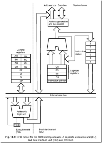
The jobs performed by the REN line are:

(a) When REN is active, it allows the bus to control a device.

The jobs performed by the SRQ line are:

(a) With its help, a device can seek the attention of the controller. Such a case arises when the device has data to send (the device is a talker) or the device is to receive data (the device is a listener).

(b) Such a request (and not a command) can be rejected by the controller if it does not have any time to service the request.

The jobs performed by the EOI line are:

(a) It can be used by the controller as a polling line.

(b) It can be asserted by the active talker to designate the end of a message.

26. Draw and explain the timing diagram showing the sequence for data transfer to take place.

Ans. The following figure shows how data transfer is effected taking the help of handshake signals.

IEEE 488 Bus 8-11-16 PM

Sequence of events that follow on the time scale (1) ⇒ (2) ⇒ (3) ⇒ (4) ⇒ (5) ⇒

(6) ⇒ (7).

The sequence of events that take place can be explained as follows:

1. Listener(s) which will accept data indicate their readiness with regard to their data acceptance via NRFD (Not Ready For Data) line. If NRFD is low, it indicates that the listener(s) is/are not ready. Only when all the listeners are ready, the NRFD line will go high.

2. The designated talker then drives all the eight input/output lines, causing valid data to be placed on them.

3. The active talker pulls the DAV (data valid) line to zero volts 2 µS after serial number (2). This 2 µS is required for the data to settle to their respective values on the data lines.

4. The listeners now pull the NRFD line to zero, which prevents any additional data transfer from being initiated. The listeners then accept data at their individual rates.

5. When all the listeners have accepted data, the NDAC line goes high.

6. When the active talker sees that NDAC line has become high, it stops driving the line and also it releases the DAV line. The talker is now in a position to put the next data on the data bus.

7. NDAC line is pulled down to zero volt by the listeners and the data is then taken ‘away’ by the listeners.

Thus the sequence of operations that take place on the time scale are (1) ⇒ (2)


The Universal Serial Bus (USB)

The Universal Serial Bus (USB)

1. Mention the data transfer rates supported by USB. Ans. USB supports three types of data transfer rates

480 Mbps (high speed)

12 Mbps (full speed)

1.5 Mbps (low speed)

2. What are the units in a USB system?

Ans. There are three units in a USB system—a USB host, a USB device and the USB cable.

A PC acts as a USB host, a scanner or printer acts as a USB device. The host and the

device are connected by the third unit that comprise the USB system—USB cable.

3. Mention some of the application areas of USB.

Ans. Depending on the data transfer rates, the universal serial bus supports a host of application areas.

Keyboards, joysticks, mice, etc. are some of the input devices that are supported by USB for low speed applications (up to 128 KB/sec.)

USB supports medium speed (128 KB/sec. to 2 MB/sec.) applications in the areas of low and high speed modems, process plant instrumentation, scanners, ZIP drives, sound cards, etc.

For high speed application ( > 2MB/sec.) areas, examples are network adapters, optical drives, low bandwidth video, etc.

4. Discuss the features and advantages of universal serial bus.

Ans. Universal serial bus is a plug-and-play facility and connects a host computer to many simultaneously accessible peripheral devices. The resources are made available via USB through a host-scheduled, token-based protocol. While the host computer and peripheral are in operations, other peripherals can be attached, configured, used and detached via this bus which is mostly not possible with others forms of computer bus.

The characteristics associated with universal serial bus are:

z Master/slave, half-duplex, timed communication bus system and is designed to

connect peripherals and external hubs.

z Master or host hub has complete control over transaction.

z Peripherals cannot initiate a communication on the USB bus.

z Supports data transfer rates up to 480 Mbps.

z Supports various types of data transfers.

z Supports real time data for voice, audio and compressed video.

z Ability to adapt to multifarious system configurations.

z Concurrent operation up to a maximum of 127 devices possible.

z Plug and play feature.

z Wide bandwidth with entire bus width can be used in case of isochronous mode.

z Peripheral devices can be ‘hot-plugged’ and ‘hot-unplugged’.

z Device identification and configuration possible very easily.

z Cabling and connection procedure very simple.

z Easy to set up and configure.

z A host of data rates possible.

z Error detection and fault recovery possible.

z Flow control embedded into the protocol.

z Non-proprietary, open standard system.

z Can be connected from PII to higher end PCs.

z Up to 8 USB connectors can be provided for new PCs.

5. Draw the schematic of a modern PC motherboard with serial and parallel ports as well as USB ports.

Ans. In modern PC motherboards, USB ports are straightway available, while such facility is made available in older PCs by inserting USB adapter cards. Fig. 10c.1 shows the modern PC version of a motherboard which has the USB ports available from it. Thus the kind of port facilities available from such a motherboard are : USB ports, Parallel ports LPT1 and serial (RS–232) ports COM1 and COM2. For implementing USB standards, PCs must have atleast Windows 98, 2000 or XP version facilities in it.

The Universal Serial Bus (USB)8-27-32 PM

6. Discuss (a) USB host (b) USB device. Ans. (a) USB host:

A USB host is comprised of the following:

z USB host controller hardware

z USB system software

z Client software

USB system software comprises controller driver, OS and USB driver, while client software has the device driver for the USB device. The USB host:

z detects attachment/detachment of USB devices.

z manages data/control information flow either way between the host and the USB devices.

z keeps track of the status information of the USB devices.

z powers USB devices which don’t have power of their own.

(b) USB device:

A USB device has the following:

z a USB bus interface hardware

z a USB logical device and

z functions, i.e., many capabilities that a USB device can provide.

Again the bus interface hardware comprises a transreceiver and a Serial Interface Engine (SIE). The former provides the electrical requirements while the latter is meant for providing the bit timings on the bus.

The functionalities of a USB device are:

z Responds to all host requests.

z Always monitors the device address in each communication and selects self when the device address matches with that sent by communication from the host.

z When it receives some data, it checks for errors in the error checking bits. If it detects errors, then it requests for retransmission of data. When the device sends data, check bits are added before sending.

7. Explain how USB interface is implemented and also indicate the USB data signals.

Ans. USB uses two lines for differential data connections (designated D+ and D–) and also two lines for supplying power to the cable— one is VBUS (nominal value +5V) and the other customary GND wire.

The Universal Serial Bus (USB)8-28-02 PM

The USB buffered interface is shown in Fig. 10c.2.

clip_image012Three lines are input to the CMOS buffers — T X D+, T X D– and OE (output enable). The data signal levels must conform to that shown in Fig. 10c.3. The logic high terminating voltage should have a value in between 3.0– 3.5 V.

Pull-up (1.5k) and pull-down (15k) resistors are placed at the input or output of a port,

shown in Fig. 10c.4, and are inserted for detection of device connections.

The Universal Serial Bus (USB)8-28-25 PM

8. Describe the USB Cable.

Ans. The cross-sectional view of the USB cable is shown in Fig. 10c.5.


The Universal Serial Bus (USB)8-29-08 PMUSB cable assemblies are available in three varieties : detachable full-speed captive and low-speed cables. The colours recommended for the cable assembly are white, grey or black.

USB cable consists of four conductors—two for power and two for data. Again two variants are there—full-speed cable and low-speed cable. Full-speed cable consists of twisted pair of conductors for signalling which is not so for low speed cables—because for the latter, noise and electro-magnetic interference are not dominant.
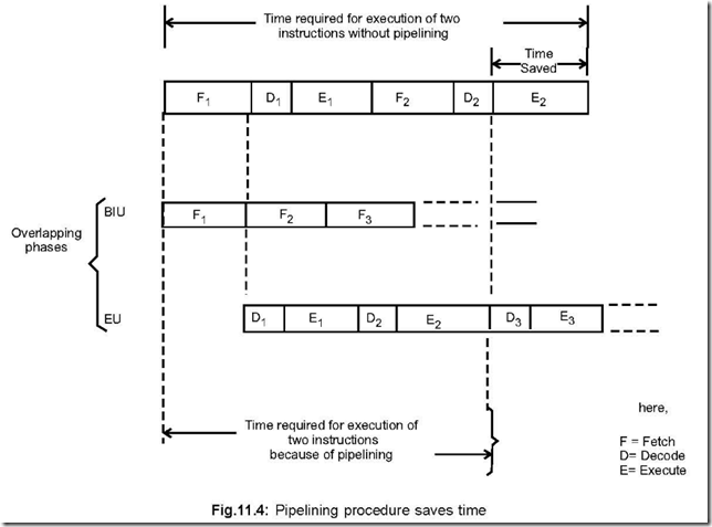
Full-speed cables may be used for low-speed purposes also—but in such a case the full-speed cable must conform to low-speed cable requirements.

9. Discuss the different types of USB connectors.

Ans. There are two types of USB connectors—Series A and Series B or Type A and Type B. ‘A’ Type connectors are used in USB devices while ‘B’ type connectors are meant for device vendors in order to provide a standard detachable cable. ‘Keyed connector’ protocol is used by USB.

Fig. 10c.6 shows a typical type ‘A’ connector, showing the standard USB icon and a top locator on the cable end side of the connector.The Universal Serial Bus (USB)8-29-26 PM

Fig. 10c.6: USB cable connector

Fig. 10c.7 and Fig.10c.8 show respectively Type A and Type B connectors whilst Fig. 10c.9 shows the signals corresponding to the pins and the recommended colour codings also.

The Universal Serial Bus (USB)8-29-54 PM

Full speed devices use B type connector allowing the device to use detachable USB cable. Thus devices can be built without hardwired cable and cable replacement becomes very easy if the need so arises.

The following gives a comparison between Type A and Type B connectors:

Type A connector

Type B connector

1. Series A plugs are always oriented towards the host.
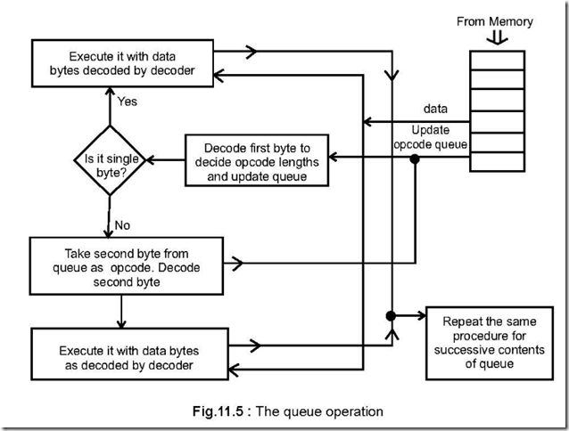
2. Series A plug mates with series A receptacle.
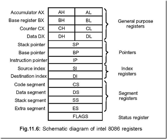
3. Series A receptacle acts as outputs from host system/hubs.

4. Series A plugs are oriented towards the host.

1. Series B plugs are always oriented towards the USB device.

2. Series B plug mates with series B receptacle.

3. Series B acts as inputs to hubs/devices.

4. Series B plugs are oriented towards the USB hub/device.

10. Draw and describe the USB topology showing the different layers or tiers. Ans. A tiered star topology is used to connect USB host and the devices and is shown in Fig. 10c.10. A maximum of 127 USB devices can be connected to one USB bus.

The Universal Serial Bus (USB)8-30-24 PM

11. Discuss bit stuffing and synchronisation field as employed in USB.

Ans. USB devices always employ encoded data for transmission and does not have a separate clock. In such a system, logic 1 is represented by no transition in signal level while logic 0 is represented by a signal transition which is effected at the beginning of the bit interval.

If a given data has long string of 1’s then no transition takes place during this period and the receiver may go out of synchronisation. In such a case, on occurrence of six consecutive 1’s, the transmitter inserts (or stuffs) a 0. Thus a signal transition is forced to occur after the sixth ‘1’ and enables synchronisation between transmitter and receiver. The receiver, on detecting such a 0, discards it.

But stuffing alone cannot always guarantee synchronisation between transmitter and receiver because the host (PC) and the device do not share the same clock. Each packet transmitted by the transmitter begins with a synchronisation field—it is a byte having the form KJKJKJKK. When the receiver detects such a field, it knows that data packets are going to come down the line. A synchronous field per packet is used.

12. How error detection and its possible elimination is done in USB?

Ans. Differential drivers and receivers are employed and shielding of cables are done to enhance data integrity in USB transmission. Error detection is done by employing CRS (Cyclic Redundancy Character) code on control and data fields. Automatic detection of attachment and detachment of devices and system level configuration of resources are some of the other facilities available in the system. Error protection fields are included in each packet of data transmitted to obviate the effects of transients. An error recovery procedure is invoked in hardware or software for cases where data integrity is of prime importance. The procedure includes retransmission of failed data a fixed number of times, beyond which the software is informed about this repeated failures. The software will then try to retrieve the data—as per the application and device function.

13. Discuss the data transfer types possible in USB.

Ans. Four types of data transfers are allowed by USB architecture. These are: control data transfers, bulk data transfers, interrupt data transfers and isochronous data transfers. These are discussed below:

Control data transfers: It is used by the USB system software when a device is first attached to the system. Apart from this, some other driver software can use the control data transfers in some special cases.

Bulk data transfers: Bulk data transfers are generally meant for printers or scanners, etc.—the data transfer being sequential in nature. Data security is ensured at the hardware level and also invoking retries a limited number of times in case of failures. Interrupt data transfers: Some event occurrence, characters, coordinates that are organised as groups of one/or a few bytes fall under this category. Such data from a device may occur at any time.

Isochronous data transfers: If data is continuous and delivered in real-time, then it

is isochronous data. This kind of data must be delivered the moment it is received.

Voice is an example of isochronous data. Two problems may arise when voice data

delivery is undertaken. Assuming data delivered at the appropriate rate by the USB

hardware, delivery delays may be there due to software-degrading real-time applications.

On the other hand, if delivery rate is not maintained, drop-outs may occur due to buffers

or frame underruns or overruns. To ensure proper data delivery, sometimes a part of

the available USB bandwidth is reserved/dedicated for isochronous data transfers.

14. Describe the clock signal associated with USB.

Ans. The clock signal associated with USB is encoded. The form of encoding undertaken is NRZI with bit stuffing. This ensures adequate transitions. Before sending each packet a SYNC field is sent. This is done for the receiver to get itself ready to synchronise itself with the bit recovery clock.

15. Describe how data is transported between host controller and devices via USB. Ans. It is the host controller (i.e., the PC) which initiates all the data transfers on USB. Up to three packets are transmitted for each bus transaction. The host controller sends a

USB packet that contains the type and direction transaction, the device address on the

USB and the endpoint number. This first packet is called a token packet and a must

whenever a transaction is initiated.

The device address which is received by each of the devices on the USB are decoded

and the one whose address matches with the address which has been sent (via the token

packet) is identified on the USB. The token packet also contains the information about

the directions of data flow—i.e., whether from a host to device or vice-versa. The source

then sends the data packet. The destination responds with a handshake packet indicating whether the transfer was successful.

16. What are the different devices available as far as device powering is concerned? Ans. There are two types of devices—bus-powered devices and self-powered devices.

Devices which depend totally on power from the cable are called bus-powered devices

while devices whose power are made available otherwise are called self-powered devices. Devices are powered by the connected hubs and this power may be available from the host controller or from an external power source.

Cables and connectors are such that upstream and downstream connectors are not interchangeable—thus loopback connections at the hubs are not feasible.

17. Show the different layers in USB architecture and discuss.

Ans. The different layers in the USB architecture are shown in Fig. 10c.11. The different layers shown in the architecture are Bus Interface Layer, Device Layer and Function Layer. The Bus Interface Layer provides physical/signalling/packet connectivity between the host and a device. This layer is the one which undertakes the actual data transfer. Each layer provides peer-to-peer connectivity. The Device Layer establishes logical connectivity between operating system software and USB logical device whereas the Function layer provides logical interconnection between the application software and USB functions.

The Universal Serial Bus (USB)8-30-57 PM

18. Discuss connection/disconnection of USB devices from the bus.

Ans. Host-connection and host-disconnection of devices from the USB is possible—this is a very vital advantage with USB which is not available with other bus systems. The host’s (PC’s)

software is thus able to recognise the connection/disconnection while it is in service and is able to reconfigure the system dynamically.

Status indicators are available on particular pins of a port attached to a hub that indicate the connection/disconnection of a USB device. The host accesses these pins to get to know the status of a device.

A device, if newly attached, is assigned a particular address by the host and it (the host) determines via software whether the newly attached device is a hub or a function.

When a device is detached from a hub’s port, the hub disables the port and indicate the host about the removal of the device. On the other hand, if the detached device is a hub the system software handles this removal of the hub(s) and or device which are connected to the removed hub.

19. What is enumeration?

Ans. The process of allocating a unique address to a unique device is called enumeration. Since attachment/detachment of devices to USB can take place at any time, hence enumeration is an on-going process as far as the USB system software is concerned.

20. What is meant by Endpoint?

Ans. Information regarding configuration, set-up or data are transported on the USB via buffers of definite size. These buffers are called endpoints. Two types of endpoints are there —IN endpoints and OUT endpoints. The host in the system delivers information into an OUT endpoint (towards the device) and the device delivers information into an IN endpoint (towards the host). An USB device can have a maximum of 16 IN and 16 OUT endpoints.

Again endpoints are of two types—data endpoint and control endpoint. Each endpoint has an unique endpoint number.

21. Discuss packets with regard to data transfer.

Ans. Information is transferred in packets in USB. Four packet types are used—token, data, handshake and start of frame packets. Each type of packet contains a combination of the following fields:

Synchronization (SYNC)

Packet ID (PID)

Address (ADDR)

Endpoint (ENDP)

Error checking (CRC) and

End of packet (EOP)

SYNC, PID and EOP are common in all the four types of packets.

SYNC is a 1-byte sequence KJKJKJKK. All packets start with SYNC field. PID is also a one byte field that identifies the type of packet being sent. The lower nibble indicates the PLD, while the upper nibble is a complement of the lower one. ADDR is a 7-bit field and contains the address of a function of the USB device for which the packet is meant.On resetting or powering on of a device, the default address becomes 0. It is reprogrammed during enumeration by the host. ENDP is a one nibble field and hence a maximum of 16 endpoints can be addressed. CRC is 5-bit/16-bit for token/data packets respectively. EOP contains two bits in SEO state and is followed by a single bit in J state.

22. Show the formats of the four types of packets and discuss them. Ans. The four types of packets are shown below in Fig. 10c.12.

The Universal Serial Bus (USB)8-32-49 PM

Token Packet: Token packet is a must for each transaction and is sent by the host controller at the beginning of each transaction. This packet indicates the type of transaction that is to take place. The ADDR (address field) is decoded by the USB device and it selects itself if the address is meant for it. Token packets can be of three types : IN, OUT and SETUP. The first indicates that the host intends to read information while the second indicates that the host would send information. SETUP indicates beginning of transfer of control.

Data Packet: A data packet may contain between 0 to 1023 bytes of data. Four types

of data packets are there : DATA0, DATA1, DATA2 and MDATA. Data transfer takes

place either way from host to device or vice-versa i.e., downstream or upstream. Handshake Packet: It is used for successful reception of data, flow control, halt condition, command acceptance/rejection, etc. It can be of three types : ACK, NAK and

STALL. ACK indicates that the packet has been successfully received while NAK

(negative acknowledgement) indicates data packet not received properly or else the receiver is busy. STALL indicates a function is unable to transmit/receive data.

Start-of-Frame Packet: It is issued by the host at the beginning of each frame. Frame transfer period is 125 µs for high speed and 1 ms for low speed or full speed bus type. The host increments the frame number each time a frame gets transferred. After reaching a value of 7FF H, the frame number rolls over.

23. Describe USB descriptors.

Ans. A hierarchy of descriptors are there for USB devices. These descriptors are data structures. They carry all the informations about a device, how the device is configured, the number as also the types of endpoints a particular device has etc.

The different descriptors are:

z Device descriptors

z Interface descriptors

z Endpoint descriptors

z Configuration descriptors

z String descriptors etc.

To note at this point that all the descriptors have a common format.


BUS STANDARDS RS:232C Standard

BUS STANDARDS

RS:232C Standard

1. What logic convention is followed in RS-232C and indicate the corresponding voltage levels also.

Ans. A negative logic convention is used for such a standard. Logical ‘1’ is represented by a transmitted voltage level in the range of –3V to –15V, while a logical ‘0’ is represented by a transmitted voltage level in the range of +3V to +15V.

2. What is the noise margin of RS-232C and how does it compare with the noise margin of TTL ICs?

Ans. The noise margin of RS-232C is 2V while that for TTL, it is 0.4V only.

The higher noise margin level of RS-232C allows it to pass through more noisy levels

than that permitted for TTL.

3. How RS-232C is interfaced with TTL?

Ans. For such an interface to be done, line drivers and receivers are required. MC 1488 accepts TTL level inputs and provides an output compatible to RS-232C. IC MC 1489 converts RS-232C levels to TTL levels.

4. What is the transition time allowed for RS-232C?

Ans. The transition time (time allowed to switch over from one voltage level to another voltage)

is 4% of one bit time. Thus at 19,200 baud, the transition time is 0.04 × 1/19,200 second= 2.1 mS.

5. What restriction does the transition time impose on the maximum cable length that can be used with RS-232C.

Ans. The transition time puts a limit on the maximum length of cable for information transformation on the RS-232C cable. As cable length increases, so also the capacitive load. This thus impedes transition time. For a baud of 19,200, the maximum cable length becomes around 5 ft.

6. Mention in which case RS-232C is used.

Ans. It is used for serial asynchronous data transmission (a) over telephone lines equipped with modems, (b) in digital systems in which the total cable distance is less than 50 ft.

7. How many pins are there on a RS-232C connector? In how many ways are they divided?

Ans. There are 25 pins on a RS-232C connector. They are divided into two groups—three (3)

wires are used for data transmission/reception purposes. Pin 2 is used for Transmitted Serial Data (TXD), pin 3 for Received Serial Data (RXD) and pin 7 for Signal Ground.

In the other group, twenty-two (22) wires are there which are used for control purposes.

The following figure shows the connections between DTE and DCE for data transmission purposes.

BUS STANDARDS 7-55-26 PM

The pin assignments of RS-232C are as here under:

1. Protective (chassis) Ground

2. Transmitted Serial data (TXD)

3. Received Serial data (RXD)

4. Request to Send (RTS)

5. Clear to Send (CTS)

6. Data Set Ready (DSR)

7. Signal Ground

8. Received Line Signal Detector (DCD)

9. (Used for Data set testing)

10. (Used for Data set testing)

11. Not Used

12. Secondary Received Line Signal detector

13. Secondary Clear to Send

14. Secondary Transmitted Data

15. Transmission Signal Element Timing (DCE Source)

16. Secondary Received Data

17. Receiver Signal Element Timing

18. Not Used

19. Secondary Request to Send

20. Data Terminal Ready

21. Signal Quality Detector

22. Ring Indicator

23. Data Signal Rate Selector (DTE/DCE Source)

24. Transmit Signal Element Timing (DTE Source)

25. Not Used

8. Indicate to what extent the 50 ft distance limitation of RS-232C can be extended. Ans. It can be extended up to 10,000 ft by using line drivers and twisted pair cables, but at the expense of reduced baud—600 only. Line drivers are signal converters and amplify the digital signals but don’t modulate them into audio signals. This use of line drivers don’t change the transmission frequency also–thus it is referred to as base band signalling.


Programmable DMA Controller (DMAC) 8257

Programmable DMA Controller (DMAC) 8257

1. Draw the pin diagram of8257.

Ans. The following figure gives the pin connection diagram of 8257.

Programmable DMA Controller (DMAC) 8257 5-54-19 PM

2. Draw the functional block diagram of8257.

Ans. The following figure shows the functional block diagram of the DMAC 8257.

As is apparent from the figure, it consists of eight blocks: data bus buffer, readlw1·ite block, control logic and mode set register, priority resolver and four channel blocks.

Programmable DMA Controller (DMAC) 8257 5-55-08 PM

3. Describe the general features of 8257. Ans. The general features of 8257 are as follows:

1. It is a 4-channel Direct Memory Access (DMA) interface IC which allows data transfer between memory and up to 4 I/O devices, bypassing CPU.

2. A maximum of 16 KB of data (= 214) can be transferred by this IC sequentially at a time. When a DMA request comes from a peripheral, the DMAC 8257, via its HRQ

(Hold Request) pin (pin number 10, which is an output pin), requests the CPU on its HOLD pin (pin number 39 of CPU 8085). CPU then acknowledges this request via its HLDA (pin 38) pin which goes to HLDA pin (pin 7) of 8257. After this, DMAC generates the required MEMR , MEMW , I/OR , I/OW signals through its 1-4 pins.

3. Initialisation of the DMAC is done under program control for each channel. The parameters which need to be initialised for each channel are starting address, number of bytes of data to be transferred, mode of operation, etc.

4. DMAC can be operated in three modes: (a) DMA Read (reading from memory, writing

into peripheral), (b) DMA Write (writing into memory, reading from peripheral),

(a) DMA verify.

5. Priority for each of the 4 channels can be set in (a) fixed priority, (b) rotating priority.

6. A Terminal Count Register exists for each of 4 channels. The number of bytes of data to be transferred is stored in the D13–D0 positions of the 16-bit Terminal Count Register. On completion of data transfer, the Terminal Count (TC) (pin 36, an output pin) goes high.

4. How many I/O devices can 8257 access? Ans. Up to 4 I/O devices can be accessed by 8257.

5. What is the maximum value of KB of data that 8257 can transfer? Ans. 8257 can transfer a maximum of 16 KB (16,384 = 214) of data.

6. What are the modes of operation of 8257? Ans. 8257 can be operated in three modes. These are:

z DMA read

z DMA write and

z DMA verify

7. Comment on priority when 8257 services the external I/Os for data transfer.

Ans. Priorities, to service the external interrupts, can be

z fixed priority.

z rotating priority.

In the Mode Set Register (it is also called control register) of 8257, D4 bit corresponds to ‘enable Rotating Priority’ bit.

If this bit is not set, then CH–0 is assigned highest priority and CH–3 lowest priority—this is by default. If D4 is set to ‘1’, the channel that has just been serviced is allocated the lowest priority. The DMA operation always assigns highest priority to CH–0.

If more than one channels are enabled, and they all place the request for DMA transfer, consecutive DMA cycles service different channels, beginning with CH–0.

8. What are the registers available with each channel of 8257?

Ans. The registers which are available with each channel of 8257 are:

z An Address Register (16-bit)

z A Terminal Count Register (TCR) (16-bit)

9. How the 8257 is initialised?

Ans. The 8257 is initialised by the CPU

(a) by loading the starting address of a DMA block for an I/O device in the 16-bit address

register.

(b) by loading D13 – D0 bits i.e., lower 14-bits of Terminal Count Register (TCR) with the number of bytes of data to be transferred.

(c) by loading D15 and D14 of TCR appropriately to set the mode of operation of 8257.

(d) by loading the Mode Set Register appropriately.

10. When does the status of pin 36 (TC = Terminal Count) of 8257 go high?

Ans. Pin 36 of 8257, which is the TC pin (an output pin, active high type) is raised high (‘1’ state) when the contents of TCR of the selected channel become zero.

11. What are meant by an enabled and a disabled peripheral?

Ans. The peripherals which are granted DMA transfer are called enabled peripherals and the

ones who are denied DMA transfer are called disabled peripherals. The above is done by Mode Set Register.

12. What are the jobs that are performed by 8257 sequentially, when it receives a request from an enabled peripheral?

Ans. 8257 does the following jobs sequentially, when it receives a request from an enabled peripheral:

(i) Gains control of the system buses, once the HOLD signal issued by 8257, is acknowledged by 8085.

(ii) 8257 sends an acknowledgement signal to the peripheral which is currently having the highest priority.

(iii) The lower 8-bits of the memory address are put out as A0 – A7 pins. These are connected to the A0 – A7 lines of the system bus. The most significant 8-bits of the memory address are put via the data bus lines D0 – D7. These are latched by 8212 latch which places them on the system address bus A8 – A15.

(iv) I/O read/write and memory read/write signals are generated.

13. Which pin of 8257 acts in a similar fashion as the ALE (address latch enable) pin of 8085? Elaborate.

Ans. Pin 8 which is ADSTB (address strobe) is an active high output pin and functions in the same manner as the ALE pin of 8085.

At the beginning of each DMA cycle, 8257 puts the most significant byte of the DMA address register on its D0 – D7 pins. These are latched by 8212 latch using the ADSTB strobe pulse of 8257. Thus at the end of this cycle, the D0 – D7 pins of 8257 can be used for data transfer purpose.

14. Where the number of bytes of data, to be transferred by DMA mode, are stored? Ans. The number of bytes of data to be transferred by DMA mode are stored in D0 – D13 bits

of Terminal Count Register (TCR). They are loaded with a value which is the required number of DMA cycles minus one.

Programmable DMA Controller (DMAC) 8257 5-55-36 PM

As shown, the two bits D15 and D14 together are loaded to set the mode of operation for that channel—like DMA write or read cycle, etc.

15. With regard to data transfer, how many classes of DMA are possible? Ans. With regard to data transfer under DMA control, two classes are possible:

(i) Sequential DMA: In this, the DMA controller reads a data byte from memory and then writes the same into I/O or vice-versa. For each of these read or write operations, 2 to 4 CLK cycles are required.

clip_image017(ii) Simultaneous DMA: It is the fastest transfer process. Here Read and Write operations are performed at the same time. Thus both MEMR and lOW (or lOR and MEMW) are active at the same time. Thus a speed improvement oftwice the sequential DMA class is possible in this case.

When bulk data is to be transferred, (i) is used while (ii) is used for moderate data transfer.

16. Why DMA mode of data transfer scheme is the fastest?

Ans. In normal data transfer schemes, a data coming from an I/0 is first taken to ACC of the CPU and then stored in memory.

But in DMA scheme, straightway data exchange takes place between memory and I/0, bypassing the ACC of CPU. Since ACC of CPU does not take part (it is absent) in DMA mode of data transfer scheme, thus this mode is fastest.

17. What are the basic building blocks of 8257? Ans. The basic building blocks are as follows:

DMA channels, Data bus buffer, Read/Write block ( I/OW , I/OR , CS, Reset, CLK, Ao – A3), control logic block (HRQ, HLDA, A4 – A7, MEMW, MEMR , Ready, ADSTB, AEN, TC, MARK) and Mode Set Register.

18. Draw the basic flowchart of a DMA mode of data transfer scheme. Ans. The flowchart will be, as shown below:

Programmable DMA Controller (DMAC) 8257 5-56-11 PM

19. What is meant by a DMA cycle?

Ans. A DMA cycle indicates the transfer of a byte.

20. Through which pin a peripheral requests the 8257 for data transfer and through which pin the peripheral gets back the acknowledgement.

Ans. A peripheral requests for data transfer to 8257 via DRQ (DRQ 0 – DRQ 3) pin and it gets back the acknowledgement via DACK ( DACK 0 – DACK 3 ) pin.

21. What determines the master or slave action of a DMA controller.

Ans. When the mP is in control of its buses (address bus, data bus and control bus), it acts as master and DMA controller acts as the slave. When DMA controller takes control of the buses, it becomes the master and mP becomes the slave.

22. What are the functions of Mode Set Register of 8257 DMA controller? Ans. The functions of the Mode Set Register are as follows:

(i) To enable/disable a channel or channels.

(ii) To configure 8257 in the following four categories: Auto Load, TC Stop, Extended

Write, Rotating Priority.

23. When DMA is undertaken, with whom the peripheral is synchronised?

Ans. When DMA is in progress, the peripheral is synchronised to the main memory, not the microprocessor.

24. When the DMA request line (i.e., HOLD pin of microprocessor) is sampled? Ans. It is sampled at the end of each machine cycle and not instruction cycle.

Thus the response time for a DMA request is a maximum of one machine cycle plus

one T state. For 8085 or Z–80 microprocessors the worst case scenario, i.e., maximum

time is 7 (seven) T states.

25. When a non-maskable interrupt is not going to be recognised by a micro- computer system?

Ans. No interrupts—either maskable or non-maskable—will be recognised during a DMA request.

26. In how many modes DMA transfer is possible?

Ans. There are three modes. These are: (a) Byte or Single mode, (b) Burst or Demand mode,

(c) Continuous or Block mode

Programmable DMA Controller (DMAC) 8257 5-56-49 PM

In byte or single mode, after transferring one byte of data, the bus control is relinquished and handed over to microprocessor.

In burst or demand mode, data is transferred till the time the peripheral is ‘ready’. After this the bus control is handed over to microprocessor.

The third method, i.e., continuous or block mode, is identical to the earlier one, but the bus control is not relinquished until the entire block of data has been transferred.

27. Which particular register is responsible for enabling (or disabling) a particular channel?

Ans. It is the shift mode set register which is responsible for enabling (or disabling) of a particular channel (CH0 to CH3). The mode set register is defined as:

Programmable DMA Controller (DMAC) 8257 5-57-50 PM

For example, if channel 1 (CH–1) is to be selected (enabled), along with TC stop option facility, then the mode set register, as per above, should have the following content:

0 1 0 0 | 0 0 1 0 = 42 H

28. How the port addresses of the registers in 8257 are done?

Ans. The port addresses of each register in 8257 are determined by the four address lines A3–A0. The port assignments for mode register, CH–1 DMA register and CH–1 count register are given below:

Programmable DMA Controller (DMAC) 8257 5-58-27 PM

It is assumed that CS signal is connected to address line A7 via an inverter and A6 – A4 are all at logic level 0.

29. Write a program to transfer ADH bytes of data from a peripheral to memory, the memory address starting from 2459H. Data to be inputed via CH–1.

Programmable DMA Controller (DMAC) 8257 5-58-54 PM

30. Which particular pin of 8257 is used to convert it into ‘master’ mode and MPU in ‘slave’ mode?

Ans. AEN (Address enable) pin of 8257 is utilised to convert it into ‘master’ mode and at the same time translate MPU into ‘slave’ mode.

31. Which particular pin of 8257 is used to interface it with a slow memory?

Ans. ‘READY’ pin of 8257 is used for the purpose. When the memory becomes ready, it sends a high signal which is connected to the ‘READY’ pin of 8257.

32. When 8267 is programmed to have fixed priority, which channel will have the lowest priority?

Ans. It is the CH-3 which will have lowest priority.

33. When data is transferred from memory to an 110, which two of the four signals 1/0R, 1/0W, MEMR, MEMW of8257 become active?

Ans. The signals which become active are MEMR and I!OW. These two signals become active low.

34. What is the function of ‘MARK’ output pin of 8257?

Ans. When this (MARK) output pin goes high, it informs the concerned VO device that the current DMA cycle is the 128th cycle since the previous MARK output.

35. Explain the Auto Load Option of the Mode Set Register of 8257.

Ans. Bit D7 is the ‘Auto Load Option’ bit of Mode Set Register 8257. It is enabled when D7

is set.

This ‘Auto Load Option’ facility is used, i.e., D7 bit of mode set register is set ( = ‘1’) when some DMA operation is repeatedly desired-like the sending of data to a CRT monitor. This is called repetitive or chained DMA operation and utilises CH-2 and CH-3.

36. What does ‘TC stop’ option do when it is set?

Ans. It is the D6 pin of mode set register. When it is set, a channel is automatically disabled when the Terminal Count output goes high. If DMA operation is to be continued or else if another operation is to begin, the channel must be enabled by a fresh Mode Set Operation in the Mode Set Register.

37. Describe the status word register of 8257.

Ans.

Programmable DMA Controller (DMAC) 8257 5-59-26 PM

The Status Word Register of 8257 is shown in Fig. 9f.6. It can be read to know the status of the terminal counts of the four channels CHO-CH3. Bit 4 corresponds to the update flag.

Any of the four bits—bit 0 to bit 3 of the status word register is set when the terminal count output corresponding to that channel goes high. When the status word is read, the TC status bits (bits 0 to 3) are cleared.

The update flag is cleared in the following cases:

z When 8257 is reset

z When ‘Auto Load’ option in the ‘Mode Set Register’ is reset.

z When it automatically goes low on the completion of update cycle.

The update flag is not affected when a status read operation is undertaken.

38. Indicate the lengths of the different registers within DMAC 8257.

Ans. 8257 has four channels. Each of these four channels has two 16-bit registers—Address Register and Terminal Count Register.

Again 8257 has two 8-bit registers—a Mode Set Register and a Status Register.

39. Describe the functions of the pins D0 – D7 (pins 21–23, 26–30).

Ans. The functions played by D0 – D7 bits are different for the following two cases: when 8257 is a slave, and when 8257 is a master.

In the ‘slave’ mode of 8257, D0 – D7 pins act as input pins. Eight bits of data at a time for the Address Register or Terminal Count Register (both 16-bits), (for a particular channel) or eight bits of data for the 8-bit Mode Set Register are received through these pins. The CPU can also read eight bits of data at a time from the Address or Terminal Count Registers or from the Status Register.

In the ‘master’ mode of 8257, the DMAC puts out the eight most significant bits of the DMA Address Register (for a particular channel), at the beginning of each DMA cycle, through D0 – D7. These are latched by 8212 latch and these latched values are put out on A8 – A15 of the system address bus. Once this operation is over, D0 – D7 pins are released so that through these pins memory data transfer can be executed for the remainder of the DMA cycle.

40. Discuss the functions of the pins A0 – A3.

Ans. Two different functions are played by these pins for the two cases when 8257 acts as the master or else as a slave.

In the master mode of 8257, these four pins A0 – A3 act as output pins. 8257 puts out the four least significant bits of the DMA Address Register on these four pins.

In the slave mode of 8257, while accessing the Mode Set Register or Status Word Register, the pins A2 A1 A0 must all be ‘0’s, while A3 = 1. Again while mode set operation is done (This is a write only operation), the status of I OW and I OR pins would be 0, 1 while for status word (this is a read only operation), the status of the above two pins would be 1, 0 respectively.

41. Explain, in detail how the Address Registers and Terminal Count Registers for each of CH0–CH3 are selected as also the Mode Set Register and Status Word Register.

Ans. The four Address Registers and four Terminal Count Registers of Channels CH0–CH3 can be accessed only if A3 = 0. For Mode Set Register and Word Register accessing, A3= 1.

For individual channel selection, bits A2 A1 are used. With 00, 01, 10, 11 values for A2 A1 select channels CH0, CH1, CH2 and CH3 respectively, while the status of bit A0 distinguishes between channel and Terminal Count Register. If A0 = 0, any of the channels would be selected and if A0 = 1 then Terminal Count Register would be selected.

The channel registers (Address Register or Terminal Count Register) of each channel are 16-bits each. Thus two operations must be performed on a channel register—one for the lower byte and the other for the upper byte to access it fully—be it reading or writing operation. This distinction between the two halves of a channel are done by a special internal First/Last F/F (F/L F/F). This F/F toggles at the completion of each READ/ WRITE operation. This F/L F/F assumes a ‘0’ state for LSB and ‘1’ for MSB accessing of a channel register.

A channel register, while being accessed, must be accessed fully—i.e., both LSB and MSB of the channel should be accessed. Therefore, before programming of a channel being initiated, the system interrupts must be disabled, otherwise an interrupt occurring after the first half of channel accessing will prevent the second half of the same channel from being accessed.

The F/L F/F is reset when 8257 gets a Reset input or whenever the Mode Set Register is programmed.

The following table shows in details how both the registers in each channel (CH0–CH3), as also the Mode Set Register and Status Word can be selected, so that they can be programmed accordingly.

Programmable DMA Controller (DMAC) 8257 6-00-02 PM

A0–A15: DMA starting address, C0–C13: Terminal Count Value (N–1), Rd and Wr: DMA verify (00), Write (01) or Read (10) Cycle selection, AL: AUTO Load, TCS: TC STOP, EW: Extended write, RP: Rotating priority, EN3–EN0: Channel enable mask, UP: Update Flag, TC3–TC0: Terminal count status bits.

42. What happens to Mode Set Register when a ‘resetting’ of the system is done?

Ans. When the system receives a ‘reset’, the mode set register is automatically cleared. It disables all the four DMA channels and inhibiting all options.

43. Compare data transfer rate of 8237 DMA and a 2 MHz 8080.

Ans. For the 8237 DMA, the data transfer rate between memory and I/O port is of the order of 1.6 MB/second while it is around 33,000 bytes/second using polling.