Intel 80486 microprocessor , Intel 80486/80386 comparison , special features of the 80486 , 80486 new instructions beyond those of the 80386 , Intel Pentium microprocessor , Pentium registers , Pentium addressing modes and instructions , Pentium versus 80486: basic differences in registers, paging, stack operations, and exceptions , Pentium input/output , applications with the Pentium , Pentium versus Pentium pro and Pentium ii/ Celeron/ Pentium ii xeon / Pentium iii / Pentium 4

11.4 Intel 80486 Microprocessor

The Intel 80486 is an enhanced 80386 microprocessor with on-chip floating-point hardware.

11.4.1 Intel80486/80386 Comparison

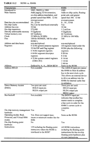
Table 11.2 compares the basic features of the 80486 with those of the 80386.

11.4.2 Special Features of the 80486

The Intel 80486 is a 32-bit microprocessor, like the Intel 80386. It executes the complete instruction set of the 80386 and the 80387DX floating-point coprocessor. Unlike the 80386, the 80486 on-chip floating-point hardware eliminates the need for an external floating-point coprocessor chip and the on-chip cache minimizes the need for an external cache and associated control logic.

image

The 80486 is object code compatible with the 8086, 8088, 80186, 80286, and 80386 processors. It can perform a complete set of arithmetic and logical operations on 8-, 16-, and 32-bit data types using a full-width ALU and eight general-purpose registers. Four gigabytes of physical memory can be addressed directly via its separate 32-bit addresses and data paths. An on-chip memory management unit is added, which maintains the integrity of memory in the multitasking and virtual-memory environments. Both memory segmentation and paging are supported.

The 80486 has an internal 8 Kbyte cache memory. This provides fast access to recently used instructions and data. The internal write-through cache can hold 8 Kbytes of data or instructions. The on-chip floating-point unit performs floating-point operations on the 32-, 64-, and 80- bit arithmetic formats specified in the IEEE standard and is object code compatible with the 8087, 80287, and 80387 coprocessors. The fetching, decoding, execution, and address translation of instructions is overlapped within the 80486 processor using instruction pipelining. This allows a continuous execution rate of one clock cycle per instruction for most instructions.

Like the 80386, the 80486 processor can operate in three modes (set in software):

real, protected, and virtual 8086 mode. After reset or power up, the 80486 is initialized in real mode. This mode has the same base architecture as the 8086, but allows access to the 32-bit register set of the 80486 processor. Nearly all of the 80486 processor instructions are available, but the default operand size is 16 bits. The main purpose of real mode is to set up the processor for protected mode.

Protected mode, or protected virtual address mode, is where the complete capabilities of the 80486 become available. Segmentation and paging can both be used in protected mode. All 8086, 80286, and 386 processor software can be run under the 80486 processor’s hardware-assisted protection mechanism.

Virtual 8086 mode is a submode for protected mode. It allows 8086 programs to be run but adds the segmentation and paging protection mechanisms of protected mode. It is more flexible to run 8086 in this mode than in real mode because virtual 8086 mode can simultaneously execute the 80486 operating system and both 8086 and 80486 processor applications.

The 80486 is provided with a bus backofffeature. Using this, the 80486 will float its bus signals if another bus master needs control of the bus during a 80486 bus cycle and then restart its cycle when the bus again becomes available. The 80486 includes dynamic bus sizing. Using this feature, external controllers can dynamically alter the effective width of the data bus with 8-, 16-, or 32-bit bus widths.

In terms of programming models, the Intel 80386 has very few differences with the 80486 processor. The 80486 processor defines new bits in the EFLAGS, CRO, and CR3 registers. In the 80386 processor, these bits were reserved, so the new architectural features should be a compatibility issue.

11.4.3 80486 New Instructions Beyond Those of the 80386

There are six basic instructions plus floating-point instructions added to the 80486 instruction set beyond those of the 80386 instruction set as follows:

1. Three New Application Instructions

  • BSWAP
  • XADD
  • CMPXCHG

2. Three New System Instructions

  • INVD
  • WBINVD
  • INVLPG

The 80386 can execute all its floating-point instructions when the 80387 is present in the system. The 80486, on the other hand, can directly execute all its floating­ point instructions (same as the 80386 floating-point instructions) because it has the on-chip floating-point hardware.

The three new application instructions included with the 80486 are BSWAP reg32; XADD dest, source; and CMPXCHG dest, source. BSWAP reg32 reverses the byte order of a 32-bit register, converting a value in little/big endian form to big/little endian form. That is, the BSWAP instruction exchanges bits 7-0 with bits 31-24 and bits 15-8 with bits 23-16 of a 32-bit register. Executing this instruction twice in a row leaves the register with the original value. When BSWAP is used with a 16-bit operand size, the result left in the destination operand is undefined. Consider an example of a 32-bit operand: If (EAX) = 12345678H, then after BSWAP EAX, the contents of EAX are 78563412H. Note that little endian is a byte-oriented method in which the bytes are ordered (left to right) as 3, 2, 1, and 0, with byte 3 being the most significant byte. Big endian on the other hand, is also a byte-oriented method where the bytes are ordered (left to right) as 0, I, 2, and 3 with byte 0 being the most significant byte. The BSWAP instruction speeds up execution of decimal arithmetic by operating on four digits at a time.

XADD dest, source has the form

image

The XADD dest, source instruction loads the destination into the source and then loads the sum of the destination and the original value of the source into the destination. For example, if (AX)= Ol23H, (BX) = 9876H, then after XADD AX, BX, the contents of AX and BX are respectively 9999H and 0123H.

CMPXCHG dest, source has the form:

imageThe CMPXCHG instruction compares the (AL, AX or EAX register) with the destination. If they are equal, the source is loaded into the destination; Otherwise, the destination is loaded into the AL,AX or EAX. For example, if (DX) = 4324H, (AX) = 4532H, and (BX) = 4532H, then after CMPXCHG BX, OX, the ZF flag is set to one and (BX) = 4324H.

11.5 Intel Pentium Microprocessor

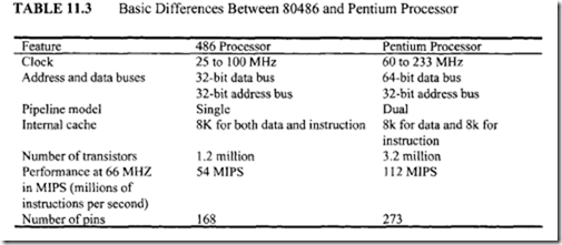
Table 11.3 summarizes the fundamental differences between the basic features of 486 and Pentium families. Microprocessors have served largely separate markets and purposes: business PCs and engineering workstations. The PCs have used Microsoft’s DOS and Windows operating systems whereas the workstations have used various features of UNIX.

image

The PCs have not been utilized in the workstation market because of their relatively modest performance, especially with regard to complicated graphics display and floating-point calculations. Workstations have been kept out of the PC market partially because of their high prices and hard-to-use system software.

The Pentium has brought the PCs up to workstation-class computational performance with sophisticated graphics. The Intel Pentium is a 32-bit microprocessor with a 64-bit data bus. The Intel Pentium, like its predecessor the Intel 80486, is 100% object code compatible with 8086/80386 systems. BICMOS(Bipolar and CMOS) technology is used for the Pentium.

The Pentium processor has three modes of operation; real-address mode (also called "real mode"), protected mode, and system management mode. The mode determines which instructions and architecture features are accessible. In real-address mode, the Pentium processor runs programs written for 8086 or for the real-address mode of an 80386 or 80486.

The architecture of the Pentium processor in this mode is identical to that of the 8086 microprocessor. In protected mode, all instruction and architectural features of the Pentium are available to the programmer. Some of the architectural features of the Pentium processor include memory management, protection, multitasking, and multiprocessing. While in protected mode, the virtual 8086 (v86) mode can be enabled for any task. For the v86 mode, the Pentium can directly execute "real-address-mode" 8086 software in a protected, multitasking environment.

The Pentium processor is also provided with a system management mode (SMM) similar to the one used in the 80486SL, which allows to design for low power usage. SMM is entered through activation of an external interrupt pin (system management interrupt, SMI#). In December 1994, Intel detected a flaw in the Pentium chip while performing certain division calculations. The Pentium is not the first chip that Intel has had problems with. The first version of the Intel 80386 had a math flaw that Intel quickly fixed before there were any complaints. Some experts feel that Intel should have acknowledged the math problem in the Pentium when it was first discovered and then have offered to replace the chips. In that case, the problem with the Pentium most likely would have been ignored by the users. However, Intel was heavily criticized by computer magazines when the division flaw in the Pentium chip was first detected.

The flaw in the division algorithm in the Pentium was caused by a problem with a look-up table used in the division. Errors occur in the fourth through the fifteenth significant

decimal digits. This means that in a result such as 5.78346, the last three digits could be incorrect. For example, the correct answer for the operation 4,195,835 – (4,195,835 + 3,145,727) + (3,145,727) is zero. The Pentium provided a wrong answer of 256. IBM claimed this problem can occur once every 24 days. Intel eventually fixed the division flaw problem in the Pentium.

The Pentium microprocessor is based on a superscalar design. This means that  the processor includes dual pipelining and executes more than one instruction per clock cycle; note that scalar microprocessors such as the 80486 family have only one pipeline and execute one instruction per clock cycle, and superscalar processors allow more than one instruction to be executed per clock cycle.

The Pentium microprocessor contains the complete 80486 instruction set along with some new ones that are discussed later. Pentium’s on-chip memory management unit is completely compatible with that of the 80486.

The Pentium includes faster floating-point on-chip hardware than the 80486.

Pentium’s on-chip floating-point hardware has been completely redesigned over the 80486. Faster algorithms provide up to ten times speed-up for common operations such as add, multiply, and load. The two instruction pipelines and on-chip floating-point unit are capable of independent operations. Each pipeline issues frequently used instructions in a single clock cycle. The dual pipelines can jointly issue two integer instructions in one clock cycle or one floating-point instruction (under certain circumstances, two floating­ point instructions) in one clock cycle.

Branch prediction is implemented in the Pentium by using two prefetch buffers, one to prefetch code in a linear fashion and one to prefetch code according to the contents of the branch target buffer (BTB), so the required code is almost always prefetched before it is needed for execution. Note that the branch addresses are stored in the branch target buffer (BTB).

There are two instruction pipelines, the U pipe and the V pipe, which are not equivalent and interchangeable. The U pipe can execute all integer and floating-point instructions, whereas the V pipe can only execute simple integer instructions and the floating-point exchange register contents (FXCH) instructions.

The instruction decode unit decodes the prefetched instructions so that the Pentium can execute them. The control ROM includes the microcode for the Pentium processor and has direct control over both pipelines. A barrel shifter is included in the chip for fast shift operations.

11.5.1 Pentium Registers

The Pentium processor includes the same registers as the 80486. Three new system flags are added to the 32-bit EFLAGS register.

11.5.2 Pentium Addressing Modes and Instructions

The Pentium includes the same addressing modes as the 80386/80486.

The Pentium microprocessor includes three new application instructions and four new system instructions beyond those of the 80486. One of the new application instruction is the CMPXCHGSB. As an example, CMPXCHGSB reg64 or mem64 compares the 64-bit value in EDX:EAX with the 64 bit contents of reg64 or mem64. If they are equal, the 64-bit value in ECX:EBX is stored in reg64 or mem64; otherwise the content ofreg64 or mem64 is loaded into EDX:EAX.

Pentium floating-point instructions execute much faster than those of the 80486 instructions.

For example, a 66-MHz Pentium microprocessor provides about three times the floating­ point performance of a 66-MHz Intel 80486 DX2 microprocessor.

11.5.3 Pentium versus 80486: Basic Differences in Registers, Paging, Stack Operations, and Exceptions

Registers of the Pentium Processor versus Those of the 80486

This section discusses the basic differences between the Pentium and 80486 control, debug, and test registers.

One new control register, CR4, is included in the Pentium. CR4 contains bits that enable certain extensions to the 80486 provided in the Pentium processor. These extensions include functions for handling certain hardware error conditions.

The Pentium processor defines the type of breakpoint access by two bits in DR7 to perform breakpoint functions such as break on instruction execution only, break on data writes only, and break on data reads or writes but not instruction fetches. The implementation of test registers on the 80486 used for testing the cache has been redesigned in the Pentium processor.

Paging

The Pentium processor provides an extension to the memory management/paging functions of the 80486 to support larger page sizes.

Stack Operations

The Pentium, 80486, and 80386 microprocessors push a different value of SP on the stack for a PUSH instruction than does the 8086. The 32-bit processors push the value of the SP before it is decremented whereas the 8086 pushes the value of the SP after it is decremented.

Exceptions

The Pentium processor implements new exceptions beyond those of the 80486. For example, a machine check exception is newly defined for reporting parity errors and other hardware errors.

External hardware interrupts on the Pentium may be recognized on different instruction boundaries due to the pipelined execution of the Pentium processor and possibly an extra instruction passing through the V pipe concurrently with an instruction in the U pipe. When the two instructions complete execution, the interrupt is then serviced. Therefore, the EIP pushed onto the stack when servicing the interrupt on the Pentium processor may be different than that for the 80486 (i.e., it is serviced later). The priority of exceptions is the same on both the Pentium and 80486.

11.5.4 Pentium Input/Output

The Pentium processor handles I/O in the same way as the 80486. The Pentium can use either standard I/O or memory-mapped I/O. Standard I/O is accomplished by using IN/OUT instructions and a hardware protection mechanism. When memory-mapped I/O is used, memory-reference instructions are used for input/output and the protection mechanism is provided via segmentation or paging.

The Pentium can transfer 8, 16, or 32 bits to a device. Like memory-mapped I/O, 16- bit ports using standard I/O should be aligned to even addresses so that all 16 bits can be transferred in a single bus cycle. Like double words in memory-mapped I/O, 32-bit ports in standard I/O should be aligned to addresses that are multiples of four. The Pentium supports I/O transfer to misaligned ports, but there is a performance penalty because an extra bus cycle must be used.

The INS and OUTS instructions move blocks of data between I/O ports and memory. The INS and OUTS instructions, when used with repeat prefixes, perform block input or output operations. The string I/O instructions can operate on byte (8-bit) strings, word (16-bit) strings, or double word (32-bit) strings. When the Pentium is running in protected mode, I/O operates as in real address mode with additional protection features.

11.5.5 Applications with the Pentium

The performance of the Pentium’s floating-point unit (FPU) makes it appropriate for wide areas of numeric applications:

  • Pentium’s FPU can accept decimal operands and produce extra decimal results of up to 18 digits. This greatly simplifies accounting programming. Financial calculations that use power functions can take advantage of exponential and logarithmic functions.
  • Many minicomputer and mainframe large simulation problems can be executed by the Pentium. These applications include complex electronic circuit simulations using SPICE and simulation of mechanical systems using finite element analysis.
  • The Pentium’s FPU can move and position machine control heads with accuracy in real time. Axis positioning can efficiently be performed by the hardware trigonometric support provided by the FPU. The Pentium can therefore be used for computer numerical control (CNC) machines.
  • The pipelined instruction feature of the Pentium processor makes it an ideal candidate for DSP (digital signal processing) and related applications for computing matrix multiplications and convolutions.
  • Other possible application areas for the Pentium include robotics, navigation, data acquisition, and process control.

11.5.6 Pentium versus Pentium Pro

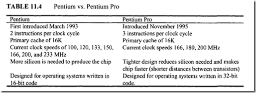
The Pentium was first introduced by Intel in March 1993, and the Pentium Pro was introduced in November 1995. The Pentium processor provides pipelined superscalar architecture. The Pentium processor’s pipelined implementation uses five stages to extract high throughput and the Pentium Pro utilizes 12-stage, superpipelined implementation, trading less work per pipestage for more stages. The Pentium Pro processor reduced its pipestage time by 33% compared with a Pentium processor, which means the Pentium Pro processor can have a 33% higher clock speed than a Pentium processor and still be equally easy to produce from a semiconductor manufacturing process. A 200-MHz Pentium Pro is always faster than a 200-MHz Pentium for 32-bit applications such as computer-aided design (CAD), 3-D graphics, and multimedia applications.

The Pentium processor’s superscalar architecture, with its ability to execute two instructions per clock, was difficult to exceed without a new approach. The new approach used by the Pentium Pro processor removes the constraint of linear instruction sequencing between the traditional "fetch" and "execute" phases, and opens up a wide instruction pool. This approach allows the "execute" phase of the Pentium Pro processor to have much more visibility into the program’s instruction stream so that better scheduling may take place. This allows instructions to be started in any order but always be completed in the original program order.

Microprocessor speeds have increased tremendously over the past 10 years, but the speed of the main memory devices has only increased by 60 percent. This increasing

image

memory latency, relative to the microprocessor speed, is a fundamental problem that the Pentium Pro is designed to solve. The Pentium Pro processor "looks ahead" into its instruction pool at subsequent instructions and will do useful work rather than be stalled. The Pentium Pro executes instructions depending on their readiness to execute and not on their original program order. In summary, it is the unique combination of improved branch prediction, choosing the best order, and executing the instructions in the preferred order that enables the Pentium Pro processor to improve program execution over the Pentium processor. This unique combination is called "dynamic execution."

The Pentium Pro does a great job running some operating systems such as Windows NT or Unix. The first release of Windows 95 contains a significant amount of 16-bit code in the graphics subsystem. This causes operations on the Pentium Pro to be serialized instead of taking advantage ofthe dynamic execution architecture. Nevertheless, the Pentium Pro is up to 30% faster than the fastest Pentium in 32-bit applications. Table

11.4 compares the basic features the Pentium with those of the Pentium Pro.

11.5.7 Pentium II/ Celeron/ Pentium II XeonTM / Pentium III / Pentium 4

The 32-bit Pentium II processor is Intel’s latest addition to the Pentium line of microprocessors, which originated form the widely cloned 80×86 line. It basically takes attributes of the Pentium Pro processor plus the capabilities of MMX technology to yield processor speeds of 333, 300, 266, and 233 MHz. The Pentium II processor uses 0.25 micron technology (this refers to the width of the circuit lines on the silicon) to allow increased core frequencies and reduce power consumption. The Pentium II processor took advantage of four new technologies to achieve its performance ratings:

  • Dual Independent Bus Architecture (DIB)
  • Dynamic Execution
  • Intel MMX Technology
  • Single-Edge-Contact Cartridge

DIB was first implemented in the Pentium Pro processor to address bandwidth limitations. The DIB architecture consists of two independent buses, an L2 cache bus and a system bus, to offer three times the bandwidth performance of single bus architecture processors. The Pentium II processor can access data from both buses simultaneously to accelerate the flow of information within the system.

Dynamic execution was also first implemented in the Pentium Pro processor.

It consists of three processing techniques to improve the efficiency of executing instructions.

These techniques include multiple branch prediction, data flow analysis, and speculative execution. Multiple branch prediction uses an algorithm to determine the next instruction to be executed following a jump in the instruction flow. With data flow analysis, the processor determines the optimum sequence for processing a program after looking at software instructions to see if they are dependent on other instructions. Speculative execution increases the rate of execution by executing instructions ahead of the program counter that are likely to be needed.

MMX (matrix math extensions) technology is Intel’s greatest enhancement to its microprocessor architecture. MMX technology is intended for efficient multimedia and communications operations. To achieve this, 57 new instructions have been added to manipulate and process video, audio, and graphical data more efficiently. These instructions support single-instruction multiple-data (SIMD) techniques, which enable one instruction to perform the same function on multiple pieces of data. Programs written using the new instructions significantly enhance the capabilities of Pentium II.

The final feature in Intel’s Pentium II processor is single-edge-contact (SEC) packaging. In this packaging arrangement, the core and L2 cache are fully enclosed in a plastic and metal cartridge. The components are surface mounted directly to a substrate inside the cartridge to enable high-frequency operation.

Intel Celeron processor utilizes Pentium II as core .The Celeron processor family includes: 333 MHz, 300A MHz, 300 MHz, and 266 MHz processors.The Celeron 266 MHz and 300 MHz processors do not contain any level 2 cache. But the Celeron 300A MHz and 333 MHz processors incorporate an integrated L2 cache. All Celeron processors are based on Intel’s 0.25 micron CMOS technology. The Celeron processor is designed for inexpensive or "Basic PC" desktop systems and can run Windows 98. The Celeron processor offers good floating-point (3D geometry calculations) and multimedia (both video and audio) performance.

The Pentium II Xeon processor contains large, fast caches to transfer data at super high speed through the processor core. The processor can run at either 400 MHz or 450 MHz. The Pentium II Xeon is designed for any mid-range or higher Intel-based server or workstation.The 450 MHz Pentium II Xeon can be used in dual-processor (two-way) workstations and servers. The 450 MHz Pentium II Xeon processor with four-way servers is expected to be available in the future.

The Pentium III operates at 450 MHz and 500 MHz. It is designed for desktop PCs. The Pentium III enhances the multimedia capabilities of the PC, including full screen video and graphics. Pentium III Xeon processors run at 500 MHz and 550 MHz. They are designed for mid-range and higher Internet-based servers and workstations. It is compatible with Pentium II Xeon processor-based platforms. Pentium III Xeon is also designed for demanding workstation applications such as 3-D visualization, digital content creation, and dynamic Internet content development. Pentium III-based systems can run applications on Microsoft Windows NT or UNIX-based environments. The Pentium III Xeon is available in a number of L2 cache versions such as 512-Kbytes, 1-Mbyte, or 2-Mbytes (500 MHz); 512 Kbytes (550 MHz) to satisfy a variety of lnternet application requirements.

The Intel Pentium 4 is an enhanced Pentium III processor. It is currently available at 1.30, 1.40, 1.50, and 1.70 GHz. The chip’s all-new internal design contains Intel Net Burst™ micro-architecture. This provides the Pentium 4 with hyper pipelined technology ( which doubles the pipeline depth to 20 stages), a rapid execution engine ( which pushes the processor’s ALUs to twice the core frequency), and 400 MHz system bus. The Pentium 4 contains 144 new instructions. Furthermore, inclusion of an improved Advanced Dynamic Execution and an improved floating point pushes data efficiently through the pipeline.

This enhances digital audio, digital video and 3D graphics. Along with other features such as streaming SIMD Extensions 2 (SSE2) that extends MMX™ technology, the Pentium 4 gives the advanced technology to get the most out of the Internet. Finally, the Pentium 4 offers high performance when networking multiple PCs, or when attaching Pentium 4 based PC to home consumer electronic systems and new peripherals.
 

80386 Instruction Set

11.3.5 80386 Instruction Set

The 80386 can execute all 16-bit instructions in real and protected modes. This is provided in order to make the 80386 software compatible with the 8086. The 80386 uses either 8- or 32-bit displacements and any register as the base or index register while executing 32-bit code. However, the 80386 uses either 8- or 16-bit displacements with the base and index registers while executing 16-bit code. The base and index registers utilized by the 80386 for 16- and 32-bit addresses are as follows:

image

In the following, the symbol ( ) will indicate the contents of a register or a memory location. A description of some of the new 80386 instructions is given next.

1. Arithmetic Instructions

There are two new sign extension instructions beyond those of the 8086.

CWDE      Sign-extend 16 bit contents of AX to a 32-bit double word in EAX.

CDQ        Sign-extend a double word (32 bits) in EAX to a quadword (64 bits) in EDX:EAX

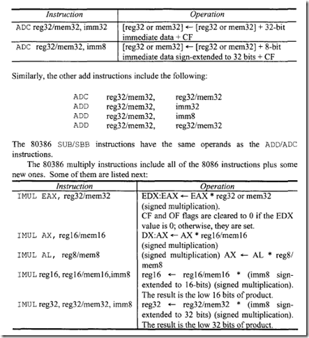
The 80386 includes all of the 8086 arithmetic instructions plus some new ones. Two of the instructions are as follows:

image

The unsigned multiplication MUL instruction has the same operands as IMUL.

The 80386 divide instructions include all of the 8086 instructions plus some new ones. Some of them are listed next:

image

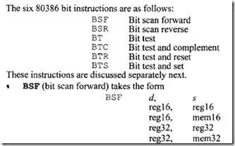
2. Bit Instructions

image

BSF scans (checks) the 16-bit (word) or 32-bit (double word) number defined by s from right to left (bit 0 to bit 15 or bit 31). The bit number of the first 1 found is stored in d. If the whole 16-bit or 32-bit number is 0, the ZF flag is set to 1; Otherwise, ZF = 0. For example, consider BSF EBX, EDX. If (EDX) = 01241240 16, then after BSF EBX, EDX, (EBX) = 00000006 16 and ZF = 0. The bit number 6 in EDX (contained in the second nibble of EDX) is the first 1 found when (EDX) is scanned from the right.

BSR (bit scan reverse) takes the form

image

BSR scans (checks) the 16-bit or 32-bit number defined by s from the most significant bit (bit 15 or bit 31) to the least significant bit (bit 0). The destination operand d is loaded with the bit index (bit number) of the first set bit. If the bits in the number are all O’s, ZF is set to 1 and operand dis undefined; ZF is reset to 0 if a 1 is found.

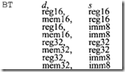
BT (bit test) takes the form

image

BT assigns the bit value of operand d (base) specified by operands (bit offset) to the carry flag. Only CF is affected. If operands is an immediate data, only 8 bits are allowed in the instruction. This operand is taken modulo 32 so that the range of immediate bit offset is from 0 to 31. This permits any bit within a register to be selected. If dis a register, the bit value assigned to CF is defined by the value of the bit number defined by s taken modulo the register size (16 or 32). If dis a memory bit string, the desired 16 bits or 32 bits can be determined by adding s (bit index) divided by the operand size (16 or 32) to the memory address of d. The bit within this 16- or 32-bit word is defined by d taken modulo the operand size ( 16 or 32). If d is a memory operand, the 80386 may access 4 bytes in memory starting at effective address plus 4 x [bit offset divided by 32]. As an example, consider BT ex, DX. If (CX) = 081F and (DX) = 0021 16,then after BT ex, DX, because the contents of DX is 3310, the bit number 1 [remainder of33/16 = 1 of CX (value 1)] is reflected in CF and therefore, CF= 1.

BTC (bit test and complement) takes the form

BTC       d,         s

where d and s have the same definitions as for the BT instruction. The bit of d defined by sis reflected in CF. After CF is assigned, the same bit of d defined by sis ones complemented. The 80386 determines the bit number from s (whether s is immediate data or register) and d (whether dis register or memory bit string) in the same way as for the BT instruction.

  • BTR (bit test and reset) takes the form

BTR         d,             s

Where d and s have the same definitions as for the BT instruction. The bit of d defined by s is reflected in CF. After CF is assigned, the same bit of d defined by s is reset to 0. Everything else applicable to the BT instruction also applies to BTR.

  • BTS (bit test and set) takes the form

BTS          d,          s

BTS is the same as BTR except that the specified bit in dis set to 1 after the bit value of d defined by sis reflected in CF. Everything else applicable to the BT instruction also applies to BTS.

3. Set Byte on Condition Instructions

These instructions set a byte to 1 or reset a byte to 0 depending on any of the 16 conditions defined by the status flags. The byte may be located in memory or in a 1-byte general register. These instructions are very useful in implementing Boolean expressions in high-level languages. The general structure of these instructions is SET cc (set byte on condition cc), which sets a byte to 1 if condition cc is true or else resets the byte to 0.

As an example, consider SETB BL (set byte if below; CF = 1). If (BL) = 5216 and CF = I, then, after this instruction is executed, (BL) = 01 16 and eF remains at I ; all other flags (OF, SF, ZF, AF, PF) are undefined. On the other hand, if eF = 0, then, after execution of this instruction, (BL) = 0016, CF = 0, and ZF = 1; all other flags are undefined. The other SET cc instructions can similarly be explained.

4. Conditional Jumps and Loops

JECXZ disp8 jumps if [ECX] = 0; disp8 means a relative address. JECxz tests the contents of the ECX register for zero and not the flags. If [ECX] = 0, then, after execution of the JECXZ instruction, the program branches with a signed 8-bit relative offset(+ 12710 to -128 10 with 0 being positive) defined by disp8. The JECXZ instruction is useful at the beginning of a conditional loop that terminates with a conditional loop instruction such as LOOPNE label. JECXZ prevents entering the loop with [ECX] = 0, which would cause the loop to execute up to 232 times instead of zero times.

The loop instructions are listed next:

image

image

The 80386 loop instructions are similar to those of the 8086 except that if the counter is more than 16 bits, the ECX register is used as the counter.

5. Data Transfer Instructions

a. Move Instructions

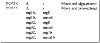
The move instructions are described as follows:

imageMOVSX reads the contents of the effective address or register as a byte or a word from the source, sign-extends the value to the operand size of the destination (16 or 32 bits), and stores the result in the destination. No flags are affected. MOVZX, on the other hand, reads the contents of the effective address or register as a byte or a word, zero-extends the value to the operand size of the destination (16 or 32 bits), and stores the result in the destination. No flags are affected. For example, consider MOVSX BX, CL. If (CL) = 8116 and (BX) = 21AF 16, then, after execution of this MOVSX, register BX contains FF81 16 and the contents of CL do not change. Now, consider MOVZX ex, OH. If (CX) = F237 16 and (DH) = 8516, then, after execution of this MOVZX, register CX contains 008516 and DH contents do not change.

b. Push and Pop Instructions

There are new push and pop instructions in the 80386 beyond those of the 8086: PUSHAO and POPAO. PUSHAO saves all 32-bit general registers (the order is EAX, ECX, EDX, EBX, original ESP, EBP, ESI, and EDI) onto the 80386 stack. PUSHAO decrements the stack pointer (ESP) by 3210 to hold the eight 32-bit values. No flags are affected. POPAO reverses a previous PUSHAO. It pops the eight 32-bit registers (the order is EDI, ESI, EBP, ESP, EBX, EDX, ECX, and EAX). The ESP value is discarded instead of loading onto ESP. No flags are affected. Note that ESP is actually popped but thrown away so that (ESP), after popping all the registers, will be incremented by 3210

c. Load Pointer Instructions

There are five instructions in the load pointer instruction category: LOS, LES, LFS, LGS, and LSS. The 80386 can have four versions for each one of these instructions as follows:

image

Note that mem 16:mem 16or mem 16:mem32 defines a memory operand containing the pointers composed of two numbers. The number to the left of the colon corresponds to the pointer’s segment selector; the number to the right corresponds to the offset. These instructions read a full pointer from memory and store it in the selected segment register:specified register. The instruction loads 16 bits into DS (for LOS) or into ES (for LES). The other register loaded is 32 bits for 32-bit operand size and 16 bits for 16-bit operand size. The 16- and 32-bit registers to be loaded are determined by the reg16 or reg32 register specified.

The three instructions LFS, LGS, and LSS are associated with segment registers FS, GS, and SS can similarly be explained.

6. Flag Control Instructions

There are two new flag control instructions in the 80386 beyond those of the 8086: PUSHFD and POPFD. PUSHFD decrements the stack pointer by 4 and saves the 80386 EFLAGS register to the new top of the stack. No flags are affected. POPFD pops the 32 bits (double word) from the top of the stack and stores the value in EFLAGS. All flags except VM and RF are affected.

7. Logical Instructions

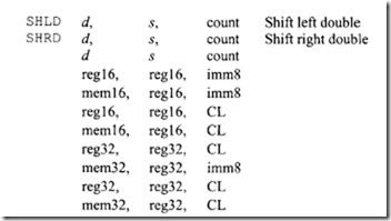
There are new logical instructions in the 80386 beyond those of the 8086:

image

For both SHLD and SHRD, the shift count is defined by the low 5 bits, so shifts from 0 to 31 can be obtained.

SHLD shifts the contents of d:s by the specified shift count with the result stored back into d; dis shifted to the left by the shift count with the low-order bits of d filled from the high-order bits of s. The bits ins are not altered after shifting. The carry flag becomes the value of the bit shifted out of the most significant bit of d. If the shift count is zero, this instruction works as an NOP. For the specified shift count, the SF, ZF, and PF flags are set according to the result in d. CF is set to the value of the last bit shifted out. OF and AF are undefined.

SHRD shifts the contents of d:s by the specified shift count to the right with the result stored back into d. The bits in dare shifted right by the shift count, with the high­ order bits filled from the low-order bits of s. The bits ins are not altered after shifting. If the shift count is zero, this instruction operates as an NOP. For the specified shift count, the SF, ZF, and PF flags are set according to the value of the result. CF is set to the value of the last bit shifted out. OF and AF are undefined.

As an example, consider SHLD BX, DX, 2. lf(BX) = 183F16 and (DX) = 0IFI 16, then, after this SHLD, (BX) = 60FC 16, (DX) = 01Fl 16, CF = 0, SF= 0, ZF = 0, and PF = 1. Similarly, the SHRD instruction can be illustrated.

8. String Instructions

a. Compare String Instructions

A new 80386 instruction, CMPS mem32, mem32 (or CMPSD) beyond the compare string instructions available with the 8086 compares 32-bit words ES:EDI (second operand) with DS:ESI and affects the flags. The direction of subtraction of CMPS is (ESI) – (EDI). The left operand (ESI) is the source, and the right operand (EDI) is the destination. This is a reverse of the normal Intel convention in which the left operand is the destination and the right operand is the source. This is true for byte (CMPSB) or word (CMPSW) compare instructions. The result of subtraction is not stored; only the flags are affected. For the first operand (ESI), DS is used as the segment register unless a segment override byte is present; for the second operand (EDI), ES must be used as the segment register and cannot be overridden. ESI and EDI are incremented by 4 if DF = 0 and are decremented by 4 if DF = 1. CMPSD can be preceded by the REPE or REPNE prefix for block comparison. All flags are affected.

b. Load and Move String Instructions

There are new load and move instructions in the 80386 beyond those of 8086. These are LODS mem32 (or LODSD) and MOVS mem32, mem32 (or MOVSD). LODSD loads the (32-bit) double word from a memory location specified by DS: ESI into EAX. After the load, ESI is automatically incremented by 4 if DF = 0 and decremented by 4 if DF = I. No flags are affected. LO DS can be preceded by the REP prefix. LODS is typically used within a loop structure because further processing of the data moved into EAX is normally required. MOVSD copies the (32-bit) double word at the memory location addressed by DS:ESI to the memory location at ES:EDI. DS is used as the segment register for the source and may be overridden. After the move, ESI and EDI are incremented by 4 if DF = 0 and are decremented by 4 if DF = 1. MOVS can be preceded by the REP prefix for block movement of ECX double words. No flags are affected.

c. String I/O Instructions

There are new string I/O instructions in the 80386 beyond those of the 8086: INS mem32, DX (or INSD) and OUTS DX, mem32 {or OUTS D). INSD inputs 32-bit data from a port addressed by the contents of DX into a memory location specified by ES:EDI. ES cannot be overridden. After data transfer, EDI is automatically incremented by 4 if DF = 0 and decremented by 4 if DF = 1. INSD can be preceded by the REP prefix for block input of ECX double words. No flags are affected. OUTSD outputs 32-bit data from a memory location addressed by DS: ESI to a port addressed by the contents of DX. DS can be overridden. After data transfer, ESI is incremented by 4 if DF = 0 and decremented by 4 if DF =

1. OUTS D can be preceded by the REP prefix for block output of ECX double words.

d. Store and Scan String Instructions

There is a new 80386 STOS mem32 (or STOSD) instruction. STOS stores the contents of the EAX register to a double word addressed by ES and EDI. ES cannot be overridden. After the storage, EDI is automatically incremented by

4 if DF = 0 and decremented by 4 if DF = I. No flags are affected. STOS can be preceded by the REP prefix for a block fill of ECX double words. There is also a new scan instruction, the SCAS mem32 (or SCASD) in the 80386. SCASD performs the 32-bit subtraction (EAX) – [memory addressed by ES and EDI]. The result of subtraction is not stored, and the flags are affected. SCASD can be preceded by the REPE or REPNE prefix for block search of ECX double words. All flags are affected.

e. Table Look-Up Translation Instruction

A modified version of the 8086 XLAT instruction is available in the 80386. XLAT mem8 (XLATB) replaces the AL register from the table index to the table entry. AL should be the unsigned index into a table addressed by DS:BX for a 16-bit address and by DS:EBX for the 32-bit address. DS can be overridden. No flags are affected.

9. High-Level Language Instructions

Three instructions, ENTER, LEAVE, and BOUND, are included in the 80386. The ENTER imm16,imm8 instruction creates a stack frame. The data imm8 defines the nesting depth of the subroutine and can be from 0 to 31. The value 0 specifies the first subroutine only. The data imm8 defines the number of stack frame pointers copied into the new stack frame from the preceding frame. After the instruction is executed, the 80386 uses EBP as the current frame pointer and ESP as the current stack pointer. The data imm16 specifies the number of bytes of local variables for which the stack space is to be allocated. If imm8 is zero, ENTER pushes the frame pointer EBP onto the stack; ENTER then subtracts the first operand imm16 from the ESP and sets EBP to the current ESP.

For example, a procedure with 28 bytes of local variables would have an ENTER 2 8 , 0 instruction at its entry point and a LEAVE instruction before every RET. The 28 local bytes would be addressed as offset from EBP. Note that the LEAVE instruction sets ESP TO EBP and then pops EBP. The 80386 uses BP (low 16 bits of EBP) and SP (low 16 bits of ESP) for 16-bit operands and uses EBP and ESP for 32-bit operands.

The BOUND instruction ensures that a signed array index is within the limits specified by a block of memory containing an upper and lower bound. The 80386 provides two forms of the BOUND instruction:

BOUND reg16,              mem32

BOUND reg32,              mem64

The first form is for 16-bit operands. The second form is for 32-bit operands and is included in the 80386 instruction set. For example, consider BOUND EDI, AD DR. Suppose (ADDR) = 32-bit lower bound d1 and (ADDR + 4) = 32 bit upper bound d". If, after execution of this instruction, (EDI) <d1 or>d, the 80386 traps to interrupt 5; otherwise, the array is accessed.

The BOUND instruction is usually placed following the computation of an index value to ensure that the limits of the index value are not violated. This permits a check to determine whether or not an address of an array being accessed is within the array boundaries when the register indirect with index mode is used to access an array element. For example, the following instruction sequence will allow accessing an array with base address in ESI, the index value in EDI, and an array lenght 50 bytes; assuming the 32-bit contents of memory location, 20000100 16 and 20000104 16 are 0 and 49, respectively:

imageExample 11.1

Determine the effect of each of the following 80386 instructions:

(a) CDQ

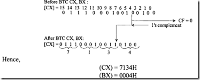
(b) BTC CX, BX

(c) MOVSX ECX, E7H

Assume (EAX) = FFFFFFFFH, (ECX) = F 1257124H, (EDX) = EEEEEEEEH, and (BX) = 0004H prior to execution of each of these given instructions.

Solution

(a) After CDQ,

(EAX) = FFFFFFFFH

(EDX) = FFFFFFFFH

(b) After BTC ex, BX, bit4 of register CX is reflected in CF and then ones complemented in CX , as is shown below.

image

(c) MOVSX ECX, E7H copies the 8-bit data E7H into the low byte of ECX and then sign­ extends to 32 bits. Therefore, after MOVSX ECX, E7H,

(ECX) = FFFFFFE7H

Example 11.2

Write an 80386 assembly language program to multiply a signed 8-bit number in AL by a signed 32-bit number in ECX. Assume that the segment registers are already initialized. Solution

imageExample 11.3

Write an 80386 assembly language program to move two columns of ten thousand 32-bit numbers from A (i) to B (i). In other words, move A (1) to B (1), A (2) to B (2), and so on.

Solution

image

image


80386 pins and signals , 80386 modes , 80386 system design and 80386 i/o

11.3.5 80386 Pins and Signals

The 80386 contains 132 pins in Pin Grid Array (PGA) or other packages.

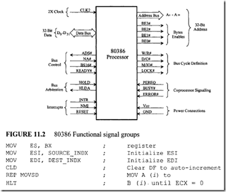
Figure 11.2 shows functional grouping of the 80386 pins. A brief description of the 80386 pins and signals is provided in the following. The # symbol at the end of the signal name or the- symbol above a signal name indicates the active or asserted state when it is low. When the symbol # is absent after the signal name or the symbol- is absent above a signal name, the signal is asserted when high.

The 80386 has 20 Vcc and 21 GND pins for power distribution. These multiple power and ground pins reduce noise. Preferably, the circuit board should contain VCC and GND planes.

CLK2 pin provides the basic timing for the 80386. This clock is then divided by 2 by the 80386 internally to provide the clock used for instruction execution. The 80386 is reset by activating the RESET pin for at least 15 CLK2 periods. The RESET signal is level­ sensitive. When the RESET pin is asserted, the 80386 will start executing instructions at address FFFF FFF0H. The 82384 clock generator provides system clock and reset signals.

D0-D31 provides the 32-bit data bus. The 80386 can transfer 16- or 32-bit data via the data bus.

The address pins A2-A31 along with the byte enable signals BEO# through BE3# are used to generate physical memory or I/O port addresses. Using the pins, the 80386 can directly address 4 gigabytes by physical memory (00000000H through FFFFFFFFH).

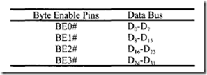
The byte enable outputs, BE0# through BE3# of the 80386, define which bytes of D0-D31 are utilized in the current data transfer. These definations are given below:

image

image

The 80386 asserts one or more byte enables depending on the physical size of the operand being transferred (1, 2, 3, or 4 bytes).

W/R#, D/C#, M/IO#, and LOCK# output pins specify the type of bus cycle being performed by the 80386. W/R# pin, when HIGH, identifies write cycle and, when LOW, indicates read cycle. D/C# pin, when HIGH, identifies data cycle, when LOW, indicates control cycle. M/ lO# differentiates between memory and I/O cycles. LOCK# distinguishes between locked and unlocked bus cycles. W/R#, DIC#, and M/10# pins define the primary bus cycle. This is because these signals are valid when ADS# (address status output) is asserted. Some of these bus cycles are listed below.

image

The 80386 bus control signals include ADS# (address status), READY# (transfer acknowledge), NA# (next address request), and BS16# (bus size 16).

The 80386 outputs LOW on the ADS# pin indicate a valid bus cycle (W!R#, Dl C#, M/lO#) and bus enable I address (BEO#-BE3#, A2-A31) signals.

When READY# input is LOW during a read cycle or an interrupt acknowledge cycle, the 80386latches the input data on the data pins and ends the cycle. When READY# is low during a write cycle, the 80386 ends the bus cycle.

The NA# input pin is activated low by external hardware to request address pipelining. BS 16# input pin permits the 80386 to interface to 32- and 16-bit memory or I/O. For 16-bit memory or 1/0, BS16# input pin is asserted low by an external device, the 80386 uses the low-order half (D0-D15) of the data bus corresponding to BEO# and BE 1# for data transfer.

BS16# is asserted high for 32-bit memory or I/O. HOLD (input) and HLDA (output) pins are 80386 bus arbitration signals. These signals are used for DMA transfers. PEREQ, BUSY#, and ERROR# pins are used for interfacing coprocessors such as 80287 or 80387 to the 80386.

There are two interrupt pins or the 80386. These are INTR (maskable) and NMI (nonmaskable) pins. NMI is leading-edge sensitive, whereas INTR is level-sensitive. When INTR is asserted and if the IF bit in the EFLAGS is 1, the 80386 (when ready) responds to the INTR by performing two interrupt acknowledge cycles and at the end of the second cycle latches an 8-bit vector on D0-D7 to identify the source of interrupt. Interrupts are serviced in a similar manner as the 8086.

11.3.6 80386 Modes

As mentioned before, the 80386 can be operated in real, protected, or virtual 8086 mode. These modes can be selected by some of the bits in the status register. Upon reset or power-up, the 80386 operates in real mode. In real mode, the 80386 can access all the 8086 registers along with the 80386 32-bit register. In real mode, the 80386 can directly address up to one megabyte of memory. The address lines A2-A 19, BEO#-BE3# are used by the 80386 in this mode.

The protected mode provides more memory space than is provided by the real mode. Furthermore, this mode supports on-chip memory management and protection features along with a multitasking operating system. Finally, the virtual 8086 mode permits the execution of8086 programs, taking full advantage of the 80386 protection mechanism. In particular, the virtual the 8086 mode allows execution of 8086 operating system and application programs concurrently with the 80386 operating system and application programs.

11.3.8 80386 System Design

In this section, the 80386 is interfaced to typical EPROM chips. As mentioned in the last section the 80386 address and data lines are not multiplexed. There is a total of thirty address pins (A2-A31) on the chip. A0 and A 1 are decoded internally to generate four byte enable outputs, BEO#, BEl#, BE2#, and BE3#. In real mode, the 80386 utilizes 20-bit addresses and A2 through A 19 address pins are active and the address pins A20 through A31 are used in real mode at reset, high for code segment (CS)-based accesses, low for others, and always low after CS changes. In the protected mode, on the other hand, all address pins A2 through A31 are active. In both modes, A0 and A 1 are obtained internally. In all modes, the 80386 outputs on the byte enable pins to activate appropriate portions of the data to transfer byte (8-bit), word ( 16-bit), and double-word (32-bit) data as follows:

image

The 80386 supports dynamic bus sizing. This feature connects the 80386 with 32- bit or 16-bit data busses for memory or I/O. The 80386 32-bit data bus can be dynamically switched to a 16-bit bus by activating the BS 16# input from high to low by a memory or I/O device. In this case, all data transfers are performed via D0-D15 pins. 32-bit transfers take place as two consecutive 16-bit transfers over data pins D0 through D15• On the other hand, the 32-bit memory or I/O device can activate the BS 16# pin HIGH to transfer data over D0-D31 pins.

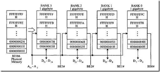
The 80386 address pins A 1 and A0 specify the four addresses of a four byte (32- bit) word. Consider the following:

image

The contents of the memory addresses which include 0, 4, 8, … with A 1A0 = 002 are transferred over D0-D7 • Similarly, the contents of addresses which include 1,5,9, …, with A 1A0 = 012 are transferred over D15 -D8• On the other hand, the contents of memory addresses 2, 6, 10, … with A 1A0 = 102 are transferred over D16-D23 while contents of addresses 3, 7, 11 … with A 1A0 = 112 are transferred over D24-D31 • Note that A 1A0 is encoded from BE3# -BEO#. The following figure depicts this:

image

In each bank, a byte can be accessed by enabling one of the byte enables, BEO# -BE3#. For example, in response to execution of a byte-MOVE instruction such as MOV [00000006H], BL, the 80386 outputs low on BE2# and high on BEO#, BEl# and BE3# and the content of BL is written to address 00000006H. On the other hand, when the 80386 executes a MOVE instruction such as MOV [ 00000004H], AX, the 80386 drives BEO# and BEl# to low. The locations 00000004H and 00000005H are written with the contents of ALand AH via D0-D7 and D8-D 15 respectively. For 32-bit transfer, the 80386 executing a MOVE instruction from an aligned address such as MOV [ 00000004H], EAX, drives all bus enable pins (BEO# -BE3#) to low and writes four bytes to memory locations 00000004H through 00000007H from EAX. Byte (8-bit), aligned word (16-bit), and aligned double-word (32-bit) are transferred by the 80386 in a single bus cycle.

The 80386 performs misaligned transfers in multiple cycles. For example, the 80386 executing a misaligned word MOVE instruction such as MOV [ 0 0 0 0 0 0 0 3H] ,AX drives BE3# to low in the first bus cycle and writes into location 00000003H (bank 3) from AL in the first bus cycle. The 80386 then drives BEO# to low in the second bus cycle and writes into location 00000004H (bank 0) from AH. This transfer takes two bus cycles.

A 32-bit misaligned transfer such as MOV [ 00000002H], EAX, on the other hand, takes two bus cycles. In the first bus cycle, the 80386 enables BE2# and BE3#, and writes the contents of low 16-bits of EAX into addresses 00000002H and 00000003H from banks 2 and 3 respectively. In the second cycle, the 80386 enables BEO# and BEl# to low and then writes the contents of upper 16-bits of EAX into addresses 00000004H and 00000005H.

In the following, design concepts associated with the 80386’s interface to memory will be discussed. The 80386 device will use 128 Kbyte, 32-bit wide memory. Four 27C256’s (32 K x 8 HCMOS EPROMs) are used.

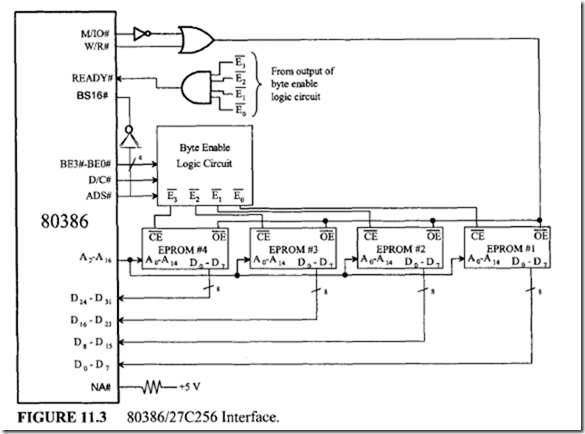
Since the 27C256 chip is 32K x 8 chip, the 80386 address lines A2-A 16 are used for addressing the 27C256’s. The 80386 M/10#, D/C#, W/R#, and BEO#-BE3# are also used. Figure 11.3 shows a simplified 80386 – 27C256 interface.

In figure 11.3, A 1 A0,BE3#-BEO#, D/C#, and ADS# pins of the 80386 are used to generate four byte enable signals, EO, E 1, E2, and E3.

The 80386 outputs low on ADS# (Address status) pin to indicate valid bus cycle (W/R#, D/C#, M/10#) and address (BEO# -BE3#) signals.

The 80386 A 1 and A0 bits (obtained internally) indicate which portion of the data bus will be used to transfer data. For example, A 1 A0 = 11 means that contents of addresses

such as 00000003H, 00000007H, … will be used by the 80386 to transfer data via its D31 -D24 pins. BE3#-BEO# and D/C# are used to produce the byte enable signals which

image

are connected to the CE pin of the appropriate EPROM. The inverted M/IO# is logically ORed with the W/R# pin. The output of this OR gate is connected to the OE pin of all four EPROM’s.

clip_image007EO, El, E2, and E3 are AND ed and connected to the READY# pin. When the READY# pin is asserted LOW, the 80386latches or reads data. Until READY# pin is asserted LOW by the external device, the 80386 inserts wait states. One must ensure that the data is ready before READY# is asserted. The BS 16# is asserted HIGH by connecting it to inverted ADS# to indicate 32-bit memory. NA# is connected to +5 V to disable pipelining.

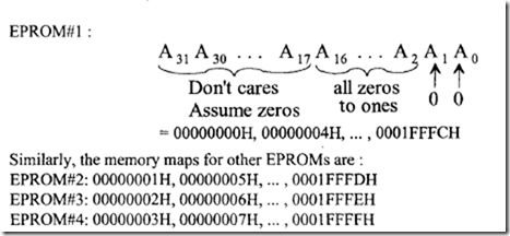
The memory map can be determined as follows:

image

11.3.9 80386 I/O

The 80386 can use either a standard I/O or a memory-mapped I/O technique.

The address decoding required to generate chip selects for devices using standard I/O is often simpler than that required for memory-mapped devices. But, memory-mapped I/O offers more flexibility in protection than standard I/O does.

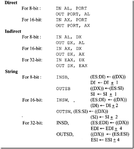
The 80386 can operate with 8-, 16-, and 32-bit peripherals. Eight-bit I/O devices can be connected to any of the four 8-bit sections of the data bus. For efficient operation, 32-bit 1/0 devices should be assigned to addresses that are even multiples of four. For standard 1/0, the 80386 includes there types of I/O instructions. These are direct, indirect, and string I/O instructions which include the following:
image


Intel and motorola 32- & 64-bit microprocessors : typical features of 32-bit and 64-bit microprocessors , intel 32-bit and 64-bit microprocessors , intel 80386 , internal80386 architecture , processing modes , basic 80386 programming model and 80386 addressing modes

INTEL AND MOTOROLA 32- & 64-BIT MICROPROCESSORS

This chapter provides a summary of the basic features of 32- and 64-bit microprocessors manufactured by Intel and Motorola. Intel 80386 and Motorola 68020 are covered in detail while an overview of the other 32-bit microprocessors is also included. Finally, a brief coverage of the 64-bit microprocessors is provided.

11.1 Typical Features of 32-bit and 64-bit Microprocessors

This section describes the basic aspects of typical 32- and 64-bit microprocessors. Topics include on-chip features such as pipelining, memory management, floating-point, and cache memory implemented in typical 32- and 64-bit microprocessors.

The first 32-bit microprocessor was Intel’s problematic iAPX432, and was introduced in 1980. Soon afterwards, the concept of "mainframe on a chip" or "micromainframe" was used to indicate the capabilities of these microprocessors and to distinguish them from previous 8- and 16-bit microprocessors.

The introduction of several 32-bit microprocessors revolutionized the microprocessor world. The performance of these 32-bit microprocessors is actually more comparable to that of superminicomputers such as Digital Equipment Corporation’s VAX11/750 and VAX11/780. Designers of 32-bit microprocessors have implemented many powerful features of these mainframe computers to increase the capabilities of the microprocessor chip sets. These include pipelining, on-chip cache memory, memory management, and floating-point arithmetic.

As mentioned in Chapter 8, pipelining is the technique in which instruction fetch and execute cycles are overlapped. This method allows simultaneous preparation for execution of one or more instructions while another instruction is being executed. Pipelining was used for many years in mainframe and minicomputer CPUs to speed up the instruction execution time of these machines. The 32-bit microprocessors implement the pipelining concept and simultaneously operate on several 32-bit words, which may represent different instructions or part of a single instruction.

Although pipelining greatly increases the rate of execution of nonbranching code, pipelines must be emptied and refilled each time a branch or jump instruction is in the code. This may slow down the processing rate for code with many branches orjumps. Thus, there is an optimum pipeline depth, which is strongly related to the instruction set, architecture, and gate density attainable on the processor chip. For many of the applications run on the 32-bit microprocessors, the three-stage pipeline is considered a reasonably optimal depth.

With memory management, virtual memory techniques, traditionally a feature of mainframes, are also implemented as on-chip hardware on typical 32-bit microprocessors.

This allows programmers to write programs much larger than those that could fit in the main memory space available to the microprocessors; the programs are simply stored on a secondary device, such as a disk drive, and portions of the program are swapped into main memory as needed.

Segmentation circuitry has been included in many 32-bit microprocessor chips.

With this technique, blocks of code called "segments," which correspond to modules of the program and have varying sizes set by the programmer or compiler, are swapped. For many applications, however, an alternative method borrowed from mainframes and superminis called "paging" is used. Basically, paging differs from segmentation in that pages are of equal sizes. Demand paging, in which the operating system automatically swaps pages as needed, can be used with all 32-bit microprocessors.

Floating-point arithmetic is yet another area in which the new chips are mimicking mainframes. With early microprocessors, floating-point arithmetic was implemented in software, largely as a subroutine. When required, execution would jump to a piece of code that would handle the tasks. This method, however, slows the execution rate considerably, so floating-point hardware, such as fast bit-slice (registers and ALU on a chip) processors and, in some cases, special-purpose chips, was developed. Other than the Intel 8087, these chips behaved more or less like peripherals. When floating-point arithmetic was required, the problems were sent to the floating-point processor and the CPU was freed to move on to other instructions while it waited for the results. The floating-point processor is implemented as on-chip hardware in typical 32-bit microprocessors, as in mainframe and minicomputer CPUs. Caching or memory-management schemes are utilized with all32-bit microprocessors in order to minimize access time for most instructions.
A cache, used for years in minis and mainframes, is a relatively small, high-speed memory installed between a processor and its main memory. The theory behind a cache is that a significant portion of the CPU time spent running typical programs is tied up in executing loops; thus, the chances are good that if an instruction to be executed is not the next sequential instruction, it will be one of some relatively small number of instructions back, a concept known as locality of reference. Therefore, a high-speed memory large enough to contain most loops should greatly increase processing rates. Cache memory is included as on-chip hardware in typical 32-bit microprocessors.

Typical 32-bit microprocessors such as Pentium and PowerPC chips are superscalar processors. This means that they can execute more than one instruction in one clock cycle. Also, some 32-bit microprocessors such as the PowerPC contain an on-chip real-time clock. This allows these processors to use modem multitasking operating systems that require time keeping for task switching and for keeping the calendar date.

A few 32-bit microprocessors implement a multiple branch prediction feature. This allows these microprocessors to anticipate jumps of the instruction flow ahead of time. Also, some 32-bit microprocessors determine an optimal sequence of instruction execution by looking at decoded instructions and then determining whether to execute or hold the instructions. Typical 32-bit microprocessors use a "look ahead" approach to execute instructions. Typical 32-bit microprocessors instruction pool for a sequence of instructions and perform a useful task rather than execute the present instruction and then go to the next.

The 64-bit microprocessors include all the features of 32-bit microprocessors. In addition, they also contain multiple on-chip integer and floating-point units, a larger address and data bus. The 64-bit microprocessors can typically execute 4 instructions per clock cycle and can run at a clock speed of more than 300 MHz.

The Pentium microprocessor is designed using a combination of mostly microprogramming (CISC–Complex Instruction Set Computer) and some hardwired control (RISC –Reduced Instruction Set Computer) whereas the PowerPC is designed using hardwired control with almost no microcode. The PowerPC is a RISC microprocessor. This means that a simple instruction set is included with PowerPC. The PowerPC instruction set includes register to register, load, and store instructions. All instructions involving arithmetic operations use registers; load and store instructions are utilized to access memory. Almost all computations can be obtained from these simple instructions. Finally, the 64-bit microprocessors are ideal candidates for data-crunching machines and high-performance desktop systems/workstations.

11.2 Intel 32-Bit and 64-Bit Microprocessors

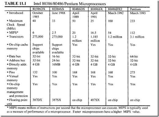
This section provides a summary of lntel 32-bit and 64-bit microprocessors. The Intel line of microprocessors has gone through many changes. The 8080/8085 (8-bit) was the first major chip by Intel but did not see major use. In 1978, Intel introduced a more powerful processor called the 8086. The 8086 is covered in detail in earlier sections of this chapter. This chip had many improved features over the 8080/85. As mentioned before, the 8086 is a 16-bit processor and utilizes pipelining. Pipelining allows the processor to execute and fetch instructions at the same time. The Intel line has progressed through the years to the 80286, 80386, 80486, and Pentium. The general trend has been an expansion of the bit width of the processors both internally and externally. The Pentium processor was introduced in 1993, and the name was changed from 80586 to Pentium because of copyright laws. The processor uses more than 3 million transistors and had an initial speed

image

of 60 MHz. The speed has increased over the years to the latest speed of233 MHz. Table

11.1 compares the basic features of the Intel 80386DX, 80386SX, 80486DX, 80486SX, 80486DX2, and Pentium. These are all32-bit microprocessors. Note that the 80386SL (not listed in the table) is also a 32-bit microprocessor with a 16-but data bus like the 80386SX. The 80386SL can run at a speed of up to 26 MHz and has a direct addressing capability of 32 MB. The 80386SL provides virtual memory support along with on-chip memory management and protection. It can be interfaced to the 80387SX to provide floating-point support. The 80386SL includes an on-chip disk controller hardware.

The Pentium microprocessor uses superscalar technology to allow multiple instructions to be executed at the same time. The Pentium uses BICMOS technology, which combines the speed of bipolar transistors and the power efficiency of CMOS technology. The internal registers are only 32 bits even though externally it has a 64-bit data bus. It has a 32-bit address bus, which allows 4 gigabytes of addressable memory space. The math coprocessor is on-chip and is up to ten times faster than the 486 in performing certain instructions. There are two execution units in the Pentium that allow the multiple execution. The multiple execution only works for instructions that are data independent, meaning that an instruction executed immediately after another using the previous result cannot be done. The Pentium uses two execution units called the "U and V pipes." Each has five pipeline stages. The U pipe can execute any of the instructions in the 80×86 set, but the V pipe executes only simple instructions. Another new feature of the Pentium is branch prediction. This feature allows the Pentium to predict and prefetch codes and advance them though the pipeline without waiting for the outcome of the zero flag.

The implementation of virtual memory is an important feature of the Pentium.

It allows a total of 64 terabytes of virtual memory. The 386/486 allowed only a 4K page size for virtual memory, but the Pentium allows either 4K or 4M page sizes. The 4K page option makes it backward compatible with the 386/486 processors. The 4M page size option allows mapping of a large program without fragmentation. It reduces the amount of page misses in virtual memory mode.

In the next section, the Intel 80386 is. covered in detail.

Table 11.1 compares the basic features of 80386, 80486, and Pentium.

11.3 Intel 80386

The Intel 80386 is Intel’s first 32-bit microprogrammed microprocessor. Its introduction in 1985 facilitated the introduction of Microsoft’s Windows operating systems. The high­ speed computer requirement of the graphical interface of Windows operating systems was supplied by the 80386. Also, the on-chip memory management of the 80386 allowed memory to be allocated and managed by the operating system. In the past, memory management was performed by software.

The Intel 80386 is a 32-bit microprocessor and is based on the 8086. A variation of the 80386 (32-bit data bus) is the 80386SX microprocessor, which contains a 16-bit data bus along with all other features of the 80386. The 80386 is software compatible at the object code level with the Intel 8086. The 80386 includes separate 32-bit internal and external data paths along with 8 general-purpose 32-bit registers. The processor can handle 8-, 16-, and 32-bit data types. It has separate 32-bit data and address pins, and generates a 32-bit physical address. The 80386 can directly address up to 4 gigabytes (232) of physical memory and 64 tetrabytes (246) of virtual memory. The 80386 can be operated from a 12.5 -, 16-, 20-, 25-, 33-, or 40-MHz clock. The chip has 132 pins and is typically housed in a pin grid array (PGA) package. The 80386 is designed using high-speed HCMOS III technology.

The 80386 is highly pipelined and can perform instruction fetching, decoding, execution, and memory management functions in parallel. The on-chip memory management and protection hardware translates logical addresses to physical addresses and provides the protection rules required in a multitasking environment. The 80386 contains a total of 129 instructions. The 80386 protection mechanism, paging, and the instructions to support them are not present in the 8086.

The main differences between the 8086 and the 80386 are the 32-bit addresses and data types and paging and memory management. To provide these features and other applications, several new instructions are added in the 80386 instruction set beyond those of the 8086.

11.3.1 Internal80386 Architecture

The internal architecture of the 80386 includes several functional units that operate in parallel. The parallel operation is known as "pipelined processing." Fetching, decoding, execution, memory management, and bus access for several instructions are performed simultaneously. Typical functional units of the 80386 are these:

  • Bus interface unit (BIU)
  • Execution unit (EU)
  • Segmentation unit
  • Paging unit

The 80386 BIU performs similar function as the 8086 BIU. The execution unit processes the instructions from the instruction queue. It contains mainly a control unit and a data unit. The control unit contains microcode and parallel hardware for fast multiplication, division, and effective address calculation. The data unit includes an ALU, 8 general-purpose registers, and a 64-bit barrel shifter for performing multiple bit shifts in one clock cycle. The data unit carries out data operations requested by the control unit. The segmentation unit translates logical addresses into linear addresses at the request of the execution unit. The translated linear address is sent to the paging unit.

Upon enabling of the paging mechanism, the 80386 translates the linear addresses into physical addresses. If paging is not enabled, the physical address is identical to the linear address and no translation is necessary. The 80386 segmentation and paging units support memory management functions. The 80386 does not contain any on-chip cache. However, external cache memory can be interfaced to the 80386 using a cache controller chip.

11.3.2 Processing Modes

The 80386 has three processing modes: protected mode, real-address mode, and virtual 8086 mode. Protected mode is the normal 32-bit application of the 80386. All instructions and features of the 80386 are available in this mode. Real-address mode (also known as "real mode") is the mode of operation of the processor upon hardware reset. This mode appears to programmers as a fast 8086 with a few new instructions. This mode is utilized by most applications for initialization purposes only. Virtual8086 mode (also called "V86 mode") is a mode in which the 80386 can go back and forth repeatedly between V86 mode and protected mode at a fast speed. When entering into V86 mode, the 80386 can execute an 8086 program. The processor can then leave V86 mode and enter protected mode to execute an 80386 program.

As mentioned, the 80386 enters real-address mode upon hardware reset. In this mode, the protection enable (PE) bit in a control register-the control register 0 (CRO)-is cleared to zero. Setting the PE bit in CRO places the 80386 in protected mode. When the 80386 is in protected mode, setting the VM (virtual mode) bit in the flag register (the EFLAGS register) places the 80386 in V86 mode.

11.3.3 Basic 80386 Programming Model

The 80386 basic programming model includes the following aspects:

  • Memory organization and segmentation
  • Data types
  • Registers
  • Addressing modes
  • Instruction set

I/O is not included as part of the basic programming model because systems designers may select to use I/O instructions for application programs or may select to reserve them for the operating system.

Memory Organization and Segmentation

The 4-gigabyte physical memory of the 80386 is structured as 8-bit bytes. Each byte can be uniquely accessed as a 32-bit address. The programmer can write assembly language programs without knowledge of physical address space. The memory organization model available to applications programmers is determined by the system software designers. The memory organization model available to the programmer for each task can vary between the following possibilities:

An address space includes a single array of up to 4 gigabytes. The 80386 maps the 4- gigabyte space into the physical address space automatically by using an address-translation scheme transparent to the applications programmers.

A segmented address space includes up to 16,383 linear address spaces of up to 4 gigabytes

each. In a segmented model, the address space is called the "logical" address space and can be up to 64 terabytes. The processor maps this address space onto the physical address space (up to 4 gigabytes by an address-translation technique).

Data Types

Data types can be byte (8-bit), word (16-bit with the low byte addressed by n and the high byte addressed by n + 1), and double word (32-bit with byte 0 addressed by n and byte 3 addressed by n + 3). All three data types can start at any byte address. Therefore, the words are not required to be aligned at even-numbered addresses, and double words need not be aligned at addresses evenly divisible by 4. However, for maximum performance, data structures (including stacks) should be designed in such a way that, whenever possible, word operands are aligned at even addresses and double word operands are aligned at addresses evenly divisible by 4. That is, for 32-bit words, addresses should start at 0, 4, 8, … for the highest speed.

Depending on the instruction referring to the operand, the following additional data types are available: integer (signed 8-, 16-, or 32-bit), ordinal (unsigned 8-, 16-, or 32-bit), near pointer (a 32-bit logical address that is an offset within a segment), far pointer (a 48-bit logical address consisting of a 16-bit selector and a 32-bit offset), string (8-, 16-, or 32-bit from 0 bytes to 232 – I bytes), bit field (a contiguous sequence of bits starting at any bit position of any byte and containing up to 32 bits), bit string (a contiguous sequence

image

of bits starting at any position of any byte and containing up to 232 – 1 bits), and packed/ unpacked BCD. When the 80386 is interfaced to a coprocessor such as the 80287 or 80387, then floating-point numbers are supported.

Registers.

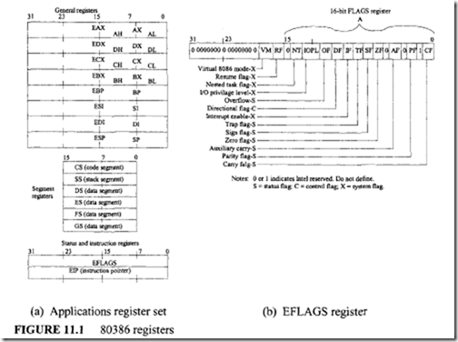
Figure 11.1 shows the 80386 registers. As shown in the figure, the 80386 has 16 registers classified as general, segment, status, and instruction pointer. The 8 general registers are the 32-bit registers EAX, EBX, ECX, EDX, EBP, ESP, ESI, and EDI. The low-order word of each of these 8 registers has the 8086 register name AX (AH or AL), BX (BH or BL), CX (CH or CL), DX (DH or DL), BP, SP, SI, and DI. They are useful for making the 80386 compatible with the 8086 processor.

The six 16-bit segment registers-CS, SS, DS, ES, FS, and GS-allow systems software designers to select either a flat or segmented model of memory organization. The purpose of CS, SS, DS, and ES is same as that of the corresponding 8086 registers. The two additional data segment registers FS and GS are included in the 80386 so that the four data segment registers (DS, ES, FS, and GS) can access four separate data areas and allow programs to access different types of data structures.

The flag register is a 32-bit register, named EFLAGS in Figure 11.1, that shows the meaning of each bit in this register. The low-order 16 bits of EFLAGS is named FLAGS and can be treated as a unit. This is useful when executing 8086 code because this part of EFLAGS is similar to the FLAGS register of the 8086. The 80386 flags are grouped into three types: status flags, control flags, and system flags.

The status flags include CF, PF, AF, ZF, SF, and OF, like the 8086. The control flag DF is used by strings like the 8086. The system flags control I/O , maskable interrupts, debugging, task switching, and enabling of virtual 8086 execution in a protected, multitasking environment. The purpose of IF and TF is identical to the 8086. Let us explain some of the system flags:

  • IOPL (VO privilege level). This 2-bit field supports the 80386 protection feature.
  • NT (nested task). The NT bit controls the IRET operation. If NT = 0, a usual return from interrupt is taken by the 80386 by popping EFLAGS, CS, and EIP from the stack. If NT== 1, the 80386 returns from an interrupt via task switching.
  • RF (resume flag). is used during debugging.
  • VM (virtual 8086 mode). When the VM bit is set to 1, the 80386 executes 8086 programs. When the VM bit is 0, the 80386 operates in protected mode.
  • The instruction pointer register (EIP) contains the offset address relative to the start of the current code segment of the next sequential instruction to be executed. The low-order 16 bits of EIP is named IP and is useful when the 80386 executes 8086 instructions.

11.3.4 80386 Addressing Modes

The 80386 has 11 addressing modes, classified into register/immediate and memory addressing modes. The register/immediate type includes 2 addressing modes, and the memory addressing type contains 9 modes.

Register/Immediate Modes

Instructions using the register or immediate modes operate on either register or immediate operands. In register mode, the operand is contained in one of the 8-, 16-, or 32- bit general registers. An example is DEC ECX, which decrements the 32-bit register ECX by 1. In immediate mode, the operand is included as part of the instruction. An example is MOV EDX, 5167 812FH, which moves the 32-bit data 5167812F 16 to the EDX register. Note that the source operand in this case is in immediate mode.

Memory Addressing Modes

The other 9 addressing modes specifY the effective memory address of an operand. These modes are used when accessing memory. An 80386 address consists of two parts: a segment base address and an effective address. The effective address is computed by adding any combination of the following four elements:

1. Displacement. The 8- or 32-bit immediate data following the instruction is the displacement; 16-bit displacements can be used by inserting an address prefix before the instruction

2. Base. The contents of any general-purpose register can be used as a base.

3. Index. The contents of any general-purpose register except ESP can be used as an index register. The elements of an array or a string of characters can be accessed via the index register.

4. Scale. The index register’s contents can be multiplied (scaled) by a factor of 1, 2, 4, or 8. A scaled index mode is efficient for accessing arrays or structures. Effective Address, EA =base register+ (index register x scale)+ displacement The 9 memory addressing modes are a combination of these four elements. Of mthe 9 modes, 8 of them are executed with the same number of clock cycles because the effective address calculation is pipelined with the execution of other instructions; the mode containing base, index, and displacement elements requires one additional clock cycle.

1. Direct mode.The operand’s effective addresses is included as part of the instruction as an 8-, 16-, or 32-bit displacement. An example is DEC WORD PTR [4000H].

2. Register indirect mode. A base or index register contains the operand’s effective address. An example is MOV EBX ,  [ECX].

3. Base mode. The contents of a base register is added to a displacement to obtain the operand’s effective address. An example is MOV [EDX + 16] , EBX.

4. Index mode. The contents of an index register is added to a displacement to obtain the operand’s effective address. An example is ADD START [EDI] , EBX.

5. Scaled index mode. The contents of an index register is multiplied by a scaling factor (1, 2, 4, or 8), and the result is added to a displacement to obtain the operand’s effective address. An example is MOV START [ EBX * 8] , ECX.

6. Based index mode. The contents of a base register is added to the contents of an index register to obtain the operand’s effective address. An example is MOV ECX 1 [ESI] [EAX].

7. Based scaled index mode. The contents of an index register is multiplied by a scaling factor (1, 2, 4, 8), and the result is added to the contents of a base register to obtain the operand’s effective address. An example is MOV [ECX *4] [EDX] , EAX.

8. Based index mode with displacement. The operand’s effective address is obtained by adding the contents of a base register and an index register with a displacement. An example is MOV [ EBX] [EB P + 0 F2 4 7 8 2AH] , ECX.

9. Based scaled index mode with displacement. The contents of an index register is multiplied by a scaling factor, and the result is added to the contents of base register and displacement to obtain the operand’s effective address. An example is MOV [ESI * 8] [EBP + 60H] , ECX.


Questions and problems

QUESTIONS AND PROBLEMS

10.1 What are the basic differences between the 68000,68008,68010, and 68012?

10.2 What D0es a HIGH on the 68000 FC2 pin indicate?

10.3

(a) If a 68000-based system operates in the user mode and an interrupt occurs, what will the 68000 mode be?

(b) If a 68000-based system operates in the supervisor mode, how can the mode be changed to user mode?

10.4

(a)  What is the purpose of 68000 trace and X flags?

(b) How can you set or reset them?

10.5 Indicate whether the following 68000 instructions are valid or not valid. Justify your answers.

image

10.6 How many addressing modes and instructions D0es the 68000 have?

10.7 What happens after execution of the following 68000 instruction?

MOVE.L D0,$03000013

10.8 What is meant by 68000 privileged instructions?

10.9 Identify the following 68000 instructions as privileged or nonprivileged:

image

image

10.11 Identify the addressing modes for each of the following 68000 instructions:

(a) CLR D0

(b) MOVE. L (Al) +,- (A5)

(c) MOVE $2000 (A2), D1

10.12 Determine the contents of registers I memory locations affected by each of the following 68000 instructions:

image

10.13 Find the contents of register D0 after execution of the following 68000 instruction sequence:

EXT.W D0

EXT.L D0

Assume [D0] = $F215A700 prior to execution of the instruction sequence.

10.14 Find the contents of D1 after execution of DIVS. W #6, D1. Assume [D1] = $FFFFFFF7 prior to execution of the 68000 instruction. Identify the quotient and remainder. Comment on the sign of the remainder.

10.15 Write a 68000 assembly program to multiply a 16-bit signed number in the low word of D0 by an 8-bit signed number in the highest byte (bits 31-24) of D0.

10.16 Write a 68000 assembly program to divide a 16-bit signed number in the high word ofD1 by an 8-bit signed number in the lowest byte ofD1.

10.17 Write a 68000 assembly program to add the top two 16 bits of the stack. Store the 16-bit result onto the stack. Assume supervisor mode.

10.18 Write a 68000 assembly program to add a 16-bit number in the low word (bits 0-15) of D 1 with another 16-bit number in the high word (bits 16-31) of D 1. Store the result in the high word of D 1.

10.19 Write a 68000 assembly program to add two 48-bit data items in memory as shown in Figure P 10.19. Store the result pointed to by A l. The operation is given by

imageFIGURE P10.19

10.20 Write a 68000 assembly program to divide a 9-bit unsigned number in the high 9 bits (bits 31-23) of D0 by 810• D0 not use any division instruction. Store the result in D0. Neglect the remainder.

10.21 Write a 68000 assembly program to compare two strings of 15 ASCII characters.

The first string is stored starting at $502030. The second string is stored at location $302510. The ASCII character in location $502030 of string 1 will be compared with the ASCII character in location $302510 of string 2, [$502031] will be compared with [$302511], and so on. Each time there is a match, store $EEEE onto the stack; otherwise, store $0000 onto the stack. Assume user mode.

10.22 Write a subroutine in 68000 assembly language to subtract two 32-bit packed BCD numbers. BCD number 1 is stored at a location starting from $500000 through $500003, with the least significant digit at $500003 and the most significant digit at $500000. BCD number 2 is stored at a location starting from $700000 through $700003, with the least significant digit at $700003 and the most significant digit at $700000. BCD number 2 is to be subtracted from BCD number 1. Store the result as packed BCD digits in D5.

10.23 Write a subroutine in 68000 assembly language to compute

imageAssume the X;’s are signed 8-bit and stored in consecutive locations starting at $504020. Assume AO points to the x;’s. Also, write the main program in 68000 assembly language to perform all initializations, call the subroutine, and then compute Z/100.

image

(b) Assume 10-MHz 68000. Write a 68000 assembly language program to obtain a delay routine for one millisecond. Using this one-millisecond routine, write a 68000 assembly language program to provide a delay for 10 seconds.

10.25 Write a 68000 assembly program to compute the following:

I= 6 xJ+ KIM

where the locations $6000, $6002, & $6004 contain the 16-bit signed integers J, K, and M. Store the result into a long word starting at $6006. Discard the remainder of KIM.

10.26 Write a subroutine in 68000 assembly language program to compute the trace of a 4×4 matrix containing 8-bit unsigned integers. Assume that each element is stored in memory as a 16-bit number with upper byte as zero in the row-major order form; that is, elements are stored in memory as row by row and within a row, elements are stored as column by column. Note that the trace of a matrix is the sum of the elements of the leading diagonal.

10.27 A 68000168230 microcomputer-based microcomputer is required to drive the LEDs connected to bit 0 of ports A and B based on the input conditions set by switches connected to bit 1 of ports A and B. The I/O conditions are as follows:

  • If the input at bit 1 of port A is HIGH and the input at bit 1 of port B is low, then the LED at port A will be ON and the LED at port B will be OFF.
  • If the input at bit 1 of port A is LOW and the input at bit 1 of port B is HIGH, then the LED at port A will be OFF and the LED at port B will be ON.
  • If the inputs of both ports A and B are the same (either both HIGH or both LOW), then both LEDs of ports A and B will be ON.

Write a 68000 assembly language program to accomplish this.

10.28 A 6800016821-based microcomputer is required to test a NAND gate. Figure PI 0.28 shows the I/O hardware needed to test the NAND gate. The microcomputer is to be programmed to generate the various logic conditions for the NAND inputs, input the NAND output, and turn the LED ON connected at bit 3 of port A if the NAND gate chip is found to be faulty. Otherwise, turn the LED ON connected at bit 4 of port A. Write 68000 assembly language program to accomplish this.

image

A 68000/68230-based microcomputer is required to add two 3-bit numbers stored in the lowest three bits of D0 and D1 and output the sum (not to exceed 9) to a common cathode seven-segment display connected at port A as shown in Figure P10.29.Write 68000 assembly language program to accomplish this by using a l00k-up table.

10.30 A 68000/68230-based microcomputer is required to input a number from 0 to 9 from an ASCII keyboard interfaced to it and output to an EBCDIC printer. Assume that the keyboard is connected to port A and the printer is connected to port B. Store the EBCDIC codes for 0 to 9 starting at an address $003030, and use this l00kup table to write a 68000 assembly language program to accomplish the above.

clip_image00810.31 Determine the status of AS, FC2-FCO, LDS, UDS, and address lines immediately after execution of the following instruction sequence (before the 68000 tristates these lines to fetch the next instruction):

MOVE #$2050,SR

MOVE.B D0,$405060

Assume the 68000 is in the supervisor mode pnor to execution of the instructions.

10.32 Suppose that three switches are connected to bits 0-2 of port A and an LED to bit 6 of port B. If the number of HIGH switches is even, turn the LED ON; otherwise, turn the LED OFF. Write a 68000 assembly language program to accomplish this.

(a) Assume a 68000/6821 system.

(b) Assume a 68000/68230 system.

10.33 Assume the pins and signal shown in Figure Pl 0.33 for the 68000, 68230 (ODD), 2764 (ODD and EVEN). Connect the chips and draw a neat schematic. Determine the memory map and I/O map (Addresses for PGCR, PADDR, PBDDR, PACR, PBCR, PADR, PBDR). Assume a 16.67-MHz internal clock on the 68000.

image

10.35 (a) Write 68000 instruction sequence so that upon hardware reset, the 68000

will initialize the supervisor stack pointer to 100010 and the program counter to 200010.

(b) Write a 68000 service routine at address $1000 for a hardware reset that will initialize all data registers to zero, address registers to $FFFFFFFF, supervisor SP to $502078, and user SP to $1F0524, and then jump to $7020F0.

10.36 Assume the 68000 stack and register values shown in Figure PI 0.36 before occurrence of an interrupt. If an external device requests an interrupt by asserting the IPL2, IPL 1, and IPLO pins with the value 0002, determine the contents of A7′ and SR during interrupt and after execution of RTE at the end of the service routine of the interrupt. Draw the memory layouts and show where A7′ points to and the stack contents during and after interrupt. Assume that the stack is not used by the service routine.

image

image

10.38  In Figure P.l0.38, ifVM > 12 V, tum an LED ON connected at bit 3 of port A. If VM < 11 V, tum the LED OFF. Using ports, registers, and memory locations as needed and level 1 autovectored interrupt:

(a) Draw a neat block diagram showing the 68000/6821 microcomputer and the connections to the diagram in Figure P10.38 to ports.

(b) Write the main program and the service routine in 68000 assembly language.

The main program will initialize ports and wait for interrupt. The service routine will accomplish the  above task and stop.

image

10.39 Write a subroutine in 68000 assembly language using the TAS instruction to find, reserve, and lock a memory segment for the main program. The memory is divided into three segments (0, 1, 2) of 16 bytes each. The first byte of each segment includes a flag byte to be used by the TAS instruction. In the subroutine, a maximum of three 16-byte memory segments must be checked for a free segment (flag byte= 0). The TAS instruction should be used to find a free segment. The starting address of the free segment (once found) must be stored in AO and the low byte D0 must be cleared to zero to indicate a free segment and the program control should return to the main program. If no free block is found, $FF must be stored in the low byte of D0 and the control should return to the main program.

10.40 Will the circuit in Figure P10.40 work? If so, determine the I/O port addresses for PGCR, PADR, PADDR, PBDR, PBDDR, PCDR and PCDDR. If not, comment briefly, modify the circuit, and then determine the port addresses. Use only the pins and the signals shown. Assume all D0n’t cares to be zeros.

image


68000 exception handlin , 68000/2732/6116/6821-based microcomputer , multiprocessine with the 68000 using the tas instruction and the as sienal .

10.13 68000 Exception Handlin :

A 16-bit microcomputer is usually capable of hanD1ing unusual or exceptional conditions. These conditions include situations such as execution of illegal instruction or division by zero. In this section, the exception-hanD1ing capabilities of the 68000 are described.

The 68000 exceptions can be divided into three groups, namely, groups 0, 1, and 2. Group 0 has the highest priority, and group 2 has the lowest priority. Within each group, there are additional priority levels. A list of 68000 exceptions along with individual priorities is as follows:

Group 0 Reset (highest level in this group}, address error (next level), and bus error (lowest level)

Group 1 Trace (highest level), interrupt (next level), illegal op-code (next level), and privilege violation (lowest level)

Group 2 TRAP, TRAPV, CHK, and ZERO DIVIDE (no individual priorities assigned in group 2)

Exceptions from group 0 always override an active exception from group 1 or group 2.

Group 0 exception processing begins at the completion of the current bus cycle (2 clock cycles). Note that the number of cycles required for a READ or WRITE operation is called a "bus cycle." This means that during an instruction fetch if there is a group 0 interrupt, the 68000 will complete the instruction fetch and then service the interrupt. Group I exception processing begins at the completion of the current instruction. Group 2 exceptions are initiated through execution of an instruction. Therefore, there are no individual priority levels within group 2. Exception processing occurs when a group 2 interrupt is encountered, provided there are no group 0 or group 1 interrupts.

When an exception occurs, the 68000 saves the contents of the program counter

and status register onto the stack and then executes a new program whose address is provided by the exception vectors. Once this program is executed, the 68000 returns to the main program using the stored values of program counter and status register.

Exceptions can be of two types: internal or external. The internal exceptions are generated by situations such as division by zero, execution of illegal or unimplemented instructions, and address error. As mentioned before, internal interrupts are called "traps." The external exceptions are generated by bus error, reset, or interrupt instructions. The basic concepts associated with interrupts, relating them to the 68000, have already been described. In this section, we will discuss the other exceptions.

In response to an exceptional condition, the processor executes a user-written program. In some microcomputers, one common program is provided for all exceptions. The beginning section of the program determines the cause of the exception and then branches to the appropriate routine. The 68000 utilizes a more general approach. Each exception can be hanD1ed by a separate program.

As mentioned before, the 68000 has two modes of operation: user state and supervisor state. The operating system runs in supervisor mode, and all other programs are executed in user mode. The supervisor state is therefore more privileged. Several privileged instructions such as MOVE to SR can be executed only in supervisor mode. Any attempt to execute them in user mode causes a trap.

We will now discuss how the 68000 hanD1es exceptions caused by external resets, trap instructions, bus and address errors, tracing , execution of privileged instructions in user mode, and execution of illegal/unimplemented instructions:

  • The reset exception is generated externally. In response to this exception, the 68000 automatically loads the initial starting address into the processor.
  • The 68000 has a TRAP instruction, which always causes an exception. The operand for this instruction varies from 0 to 15. This means that there are 16 TRAP instructions. Each TRAP instruction has an exception vector. TRAP instructions are normally used to call subroutines in an operating system. Note that this automatically places the 68000 in supervisor state. TRAPs can also be used for inserting breakpoints in a program. Two other 68000 instructions cause traps if a particular condition is true: TRAPV and CHK. TRAPV generates an exception if the overflow flag is set. The TRAPV instruction can be inserted after every arithmetic operation in a program in order to cause a trap whenever there is the possibility of an overflow. A routine can be written at the vector address for the TRAPV to indicate to the user that an overflow has occurred. The CHK instruction is designed to ensure that access to an array in memory is within the range specified by the user. If there is a violation ofthis range, the 68000 generates an exception.
  • A bus error occurs when the 68000 tries to access an address that D0es not belong to the devices connected to the bus. This error can be detected by asserting the BERR pin on the 68000 chip by an external timer when no DTACK is received from the device after a certain period of time. In response to this, the 68000 executes a user-written routine located at an address obtained from the exception vectors. An address error, on the other hand, occurs when the 68000 tries to read or write a word (16 bits) or long word (32 bits) in an odd address. This address error has a different exception vector from the bus error.
  • The trace exception in the 68000 can be generated by setting the trace bit in the status register. In response to the trace exception, the 68000 causes an internal exception after execution of every instruction. The user can write a routine at the exception vectors for the trace instruction to display register and memory contents. The trace exception provides the 68000 with the single-stepping

imagedebugging feature.

  • As mentioned before, the 68000 has privileged instructions, which must be executed in supervisor mode. An attempt to execute these instructions causes privilege violation.
  • Finally, the 68000 causes an exception when it tries to execute an illegal or unimplemented instruction.

10.14 68000/2732/6116/6821-Based Microcomputer

Figure I 0.25 shows the schematic of a 68000-based microcomputer with a 4K EPROM, a 4K static RAM, and four 8-bit I/O ports. Let us explain the various sections of the hardware schematic. Two 2732 and two 6116 chips are required to obtain the 4K EPROM and 4K RAM. The LDS and UDS pins are ORed with the memory select signal to enable the chip selects for the EPROMs and the RAMs. Address decoding is accomplished by using a 3 x 8 decoder. The decoder enables the memory or the I/O chips depending on the status of address lines A 12-A14 and the AS line of the 68000. AS is used to enable the decoder. I;; selects the EPROMs, I;" selects the RAMs, and I; selects the I/O ports.

When addressing memory chips, the DTACK input of the 68000 must be asserted for data acknowledge. The 68000 clock in the hardware schematic is 10 MHz. Therefore, each clock cycle is I 00 ns. In Figure I 0.25, AS is used to enable the 3 x 8 decoder. The outputs of the decoder are gated to assert 68000 DTACK. This means that AS is indirectly

image

used to assert DTACK. From the 68000 read timing diagram, AS goes to LOW after approximately 2 cycles (200 ns for the 10-MHz clock) from the beginning of the bus cycle. With no wait states, the 68000 samples DTACK at the falling edge of S4 (300 ns) and, if DTACK is recognized, the 68000 latches data at the falling edge of S6 (400 ns). If DTACK is not recognized at the falling edge of S4, the 68000 inserts a !-cycle (I 00 ns in this case) wait state, samples DTACK at the end of S6, and, if DTACK is recognized, latches data at the end ofS8 (500 ns), and the process continues. Because the access time of the 2732 is 200 ns (Used to be 450ns), data will not be available at the output pins of the 2732’s until after approximately 400 ns. To be on the safe side, DTACK recognition by the 68000 at the falling edge of S6 (400 ns) and latching of data at the falling edge of S8 (500 ns) will definitely satisfy the timing requirement. This means that the decoder output fo for EPROM select should go to LOW at the end of S6. Therefore, 200ns delay (Two cycles) for DTACK is assumed.

A delay circuit, as shown in Figure I 0.26, is designed using two D flip-flops.

EPPOM select activates the delay circuit. The input is then shifted right 2 bits to obtain a 2- cycle wait state to allow sufficient time for data transfer. DTACK assertion and recognition are delayed by 2 cycles during data transfer with EPROMs. Figure 10.27 shows the timing diagram for the DTACK delay circuit. Note that DTACK goes to Low after about 2 cycles if asserted by AS providing erronous result. Therefore, DTACK must be delayed.

When the EPROM is not selected by the decoder, the clear pin is asserted (output of inverter), so Q is forced LOW and Q is HIGH. Therefore, DTACK is not asserted. When the processor selects the EPROMs, the output of the inverter is HIGH, so the clear pin is not asserted. The D flip-flop will accept a high at the input, and Q2 will be HIGH and Q2 will be LOW. Now that Q2 is LOW, it can assert DTACK. Ql will provide one wait cycle and Q2 will provide two wait cycles. Because the 2732 EPROM has a 200-ns access time and the microprocessor is operating at 10 MHz (I00-ns clock cycle), two wait cycles are inserted before asserting DTACK (2 x 100 = 200 ns). Therefore, Q2 can be connected to the DTACK pin through an AND gate. No wait state is required for RAMs because the access time for the RAMs is only 120 nanoseconds.

Four 8-bit I/O ports are obtained by using two 6821 chips. When the I/O ports are selected, the VPA pin is asserted instead of DTACK. This will acknowledge to the 68000 that it is addressing a 6800-type peripheral. In response, the 68000 will synchronize all data transfer with the E clock.

The memory and I/O maps for the schematic are as follows:

  •  Memory Maps (all numbers in hex). A23 – A 16 are D0n’t cares and assumed to be 0’s .

image

image

Note that, upon hardware reset, the 68000 loads the supervisor SP high and low words, respectively, from addresses $000000 and $000002 and the PC high and low words, respectively, from locations $000004 and $000006. The memory map contains these reset vector addresses in the even and odd 2732 chips.

  • Memory Mapped I/O (all numbers in hex). A23-A16 and A 12-A3 are D0n’t cares and assumed to be 0’s.

image

For both memory and I/O chips, AS, UDS and LDS must be used in chip select logic. Note that:

1. For memory, both even and odd chips are required. However, for I/O chips, an odd-addressed I/O chip, an even-addressed I/O chip, or both can be used, depending on the number of ports required in an application. UDS and/or LDS must be used in I/O chip select logic depending on the number of IIO chips used. The same chip select logic must be used for both the even and its corresponding odd memory chip.

2. DTACK must be connected to an external input (typically a signal from the address decoding logic) to satisfy the timing requirements. In many instances, AS is directly connected to DTACK.

3. The 68000 must be connected to ROMs I EPROMs I PPROMs in such a way that the 68000 RESET vector address is included as part of the memory map.

10.15 Multiprocessine with the 68000 Using theTAS Instruction and the AS Sienal

clip_image015Earlier, the 68000 TAS instruction was discussed. The TAS instruction supports the software aspects of interfacing two or more 68000’s via shared RAM. When TAS is executed, the 68000 AS pin stays low. During both the read and write portions of the cycle, AS remains LOW and the cycle starts as the normal read cycle. However, in the normal read, AS going inactive indicates the end of the read. During execution of TAS, AS stays LOW throughout the cycle, so AS can be used in the design as a bus-locking circuit. Due to the bus locking, only one processor at a time can perform a TAS operation in a multiprocessor system.The TAS instruction supports multiprocessor operations (globally shared resources) by checking a resource for availability and reserving or locking it for use by a single processor.

The TAS instruction can, therefore, be used to allocate free memory spaces . The TAS instruction execution flowchart for allocating memory is shown in Figure 10.28. The shared RAM of the Figure 10.28 is divided into M sections. The first byte of each section will be pointed to by (EA) of theTAS (EA) instruction. In the flowchart of Figure 10.28, (EA) first points to the first byte of section 1. The instruction TAS (EA) is the executed. The TAS instruction checks the most significant bit (N bit) in (EA). N = 0 indicates that section 1 is free; N = 1 means that section 1 is busy. If N = 0, then section 1 will be allocated for use. If N = 1 (section 1 is busy), then a program will be written to subtract one section length from (EA) to check the next section for availability. Also, (EA) must be checked with the value TASLOCM. If (EA) < TASLOCM, then no space is available for allocation. However, if (EA) > TASLOCM, then TAS is executed and the availability of that section is determined.

clip_image016In a multiprocessor environment, the TAS instruction provides software support for interfacing two or more 68000’s via shared RAM. The AS signal can be used to provide the bus-locking mechanism.

Example 10.18

Assume that the 68000127321611616821 microcomputer shown in Figure 10.29 is required to perform the following:

(a) If Vx > Vy , tum the LED ON if the switch is open; otherwise tum the LED OFF. Write a 68000 assembly language program starting at address $000300 to accomplish the above by inputting the comparator output via bit 0 of Port B. Use Port A address= $002000, Port B address = $002004, CRA = $002002, CRB = $002006. Assume the

image

LED is OFF initially.

(b) Repeat part (a) using autovector level 7 and nonautovector (Vector $40). Use Port A (address $002000) for LED and switch as above with CRA=$002002. Assume supervisor mode. Write the main program and service routine in 68000 assembly language starting at addresses $000300 and $000A00 respectively. Also, initialize the supervisor stack pointer at $001200.

Solution

(a) Using Programmed I/O

From figure 10.29, the following 68000 assembly language program can be written:

image

image

image

Using Nonautovectoring (vector $40)

Figure 10.31 shows the pertinent connections for nonautovectoring interrupt.

image


68000 memory interface , 68000 i/o , 68000 programmed i/o , 68000/6821 interface , 68000/68230 interface , 68000 interrupt system , external interrupts , internal interrupts , 68000 interrupt map , 68000 interrupt address vector , an example of autovector and nonautovector interrupts , interfacing a typical aid converter to the 68000 using autovector and nonautovector interrupts and 68000 dma .

10.10 68000 Memory Interface

clip_image001One of the advantages of the 68000 is that it can easily be interfaced to memory chips with various speeds because it goes into a wait state if DTACK is not asserted (LOW) by the memory devices at the end of S4. A simplified schematic showing an interface of a 68000 to two 2732’s and two 6116’s is given in Figure 10.15. As mentioned in Chapter 9, the 2732 is a 4K x 8 EPROM and the 6116 is a 2K x 8 static RAM. The pin diagrams of the 6116 and 2732 are provided in Appendices C and E respectively. For a 4-MHz clock, each cycle is 250 ns. Because the 68000 samples data at the falling edge of S4 (750 ns) and latches data at the falling edge of S6 (1000 ns), AS can be used to assert DTACK. From the 68000 timing diagram of Figure 10.13, AS goes to LOW after approximately two cycles (500 ns). The time delay between AS going LOW and the falling edge of S6 is 500 ns. Note that LDS and UDS must be used as chip selects as in Figure 10.15. They must not be connected to AO of the memory chips. Because in that case half of the memory in each memory chip would be wasted. Note that LDS and UDS also go to LOW after about two cycles (500 ns).

In Figure 10.15, a delay circuit for DTACK is not required because the 2732 and 6116 both place data on the bus lines before the 68000 latches data. This is because the 68000 clock frequency is 4 MHz in this case. Thus, each clock cycle is 250 ns. The access times of the 2732 and 6116 are 200 ns and 120 ns respectively. Because DTACK is sampled after 3 clock cycles (3 x 250 ns = 750 ns), both the 2732 and 6116 will have adequate time to place data on the bus for the 68000 to latch.

For example, consider the even 2732 EPROM of Figure 10.16. UDS and AS are NORed and then NANDed with inverted A 13 to select this chip. With the 200-ns access time of the 2732 (Used to be 450ns), data will be placed on the 68000 D8-D15 pins after approximately 720 nanoseconds (500 ns for AS or UDS + 10 ns for the NOR gate+ 10 ns for the NAND gate+ 200 ns for the 2732). Therefore, no delay circuit for the 68000 DTACK

image

is required because the 68000 latches data from the D8-D15 pins after 4 cycles (1000 ns in this case). The timing parameters of the 68000-2732 with various 68000 frequencies are shown in Table 10.14.

Next, consider odd 6116 static RAM (SRAM) with a 4-MHz 68000. Note that the 6116 signals, W (Write enable), G (Output enable), and E (Chip enable) are decoded as follows: when G = 0 and E = 0, then W = 1 for read and W = 0 for write. In this case, LDS and AS are NORed and NANDed with A 13 to select this chip. With the 120-ns access time of the 6116 RAM, data will be placed on the 68000 D0-D7 pins after approximately 640 ns. Because the 68000 latches data after four cycles (1000 ns in this case), no delay circuit for DTACK is required. The requirements for DTACK for 68000/6116 for various 68000 clock frequencies can similarly be determined.

In case a delay circuit for DTACK is required, a ring counter with D flip-flops can be used. Let us now determine the memory maps. Figure I 0.16 shows the 68000 interface to even 2732 obtained from Figure 10.15. When A 13 = 0, UDS = 0, AS= 0, and R/W =1, the 2732 will be selected by the 68000 to read data from the 68000 DcD 15 pins. The 68000 address pins A23-A 14 are D0n’t cares (assume 0). The memory map for the even 2732 can be determined as follows:

image

In the above, for 6116’s, A 12 and A 14 – A23 are Don’t cares (assume O’s). Static RAMs such as 6116 are used for small memory system. Note that RAMs are needed when subroutines and interrupts requiring stack are desired in an application. Microprocessors requiring larger RAMs use dynamic RAMs (DRAMs). Concepts associated with interfacing DRAMs to 68000 will be discussed next.

DRAMs are typically used when memory requirements are 16k words or larger. DRAM is addressed via row and column addressing. For example, one megabit DRAM requiring 20 address bits is addressed using I 0 address lines and two control lines, RAS (Row Address Strobe) and CAS ( Column Address Strobe). To provide a 20-bit address into the DRAM, a LOW is applied to RAS and 10 bits of the address are latched. The other 10 bits of the address are applied next and CAS is then held LOW.

The addressing capability of the DRAM can be increased by a factor of 4 by adding one more bit to the address line. This is because one additional address bit results into one additional row bit and one additional column bit. This is why DRAMs can be expanded to larger memory very rapiD1y with inclusion of additional address bits. External logic is required to generate the RAS and CAS signals, and to output the current address bits to the DRAM.

DRAM controller chips take care of refreshing and timing requirements needed by the DRAMs. DRAMs typically require 4 millisecond refresh time. The DRAM controller perfonns its task independent of the microprocessor. The DRAM controller sends a wait

imagesignal to the microprocessor if the microprocessor tries to access memory during a refresh cycle.

Because of large memory, the address lines should be buffered using 74LS244 or 74HC244 (Unidirectional buffer), and data lines should be buffered using 74LS245 or 74HC245 (Bidirectional buffer) to increase the drive capability. Also, typical multiplexers such as 74LS 157 or 74HC 157 can be used to multiplex the microprocessor’s address lines into separate row and column addresses.

10.12 68000 I/O

This section covers the I/O techniques associated with the Motorola 68000.

10.12.1 68000 Programmed I/O

As mentioned before, the 68000 uses memory-mapped I/O. Data transfer using I/O ports (programmed I/O) can be achieved in the 68000 in one of the following ways:

  • By interfacing the 68000 with an inexpensive slow 6800 I/O chip such as the MC6821.
  • By interfacing the 68000 with its own family of I/O chips such as the MC68230.

image

68000/6821 Interface

The Motorola 6821 is a 40-pin peripheral interface adapter (PIA) chip. It is provided with an 8-bit bidirectional data bus (D0-D7), two register select lines (RSO, RS 1), read/write (R/W) and reset (RESET) lines, an enable line (E), two 8-bit I/O ports (PAO-PA 7), and (PBO-PB7), and other pins. Figure 10.17 shows the pin diagram of the 6821. There are six 6821 registers. These include two 8-bit ports (ports A and B), two data direction registers, and two control registers. Selection of these registers is controlled by the RSO and RS 1 inputs together with bit 2 of the control register. Table 10.15 shows how the registers are selected. In Table I 0.15, bit 2 in each control register (CRA-2 and CRB-2) determines selection of either an I/O port or the corresponding data direction register when the proper register select signals are applied to RSO and RS 1. A 1 in bit 2 in CRA or CRB allows access of I/O ports; a 0 in bit 2 of CRA or CRB selects the data direction registers.

Each I/O port bit can be configured to act as an input or output. This is accomplished by sending a 1 in the corresponding data direction register bit for those bits that are to be output and a 0 for those bits that are to be inputs. A LOW on the RESET pin clears all PIA registers to 0. This has the effect of configuring PAO-PA 7 and PBO-PB7 as inputs.

Three built- in signals in the 68000 provide the interface with the 6821: enable (E), valid memory address (VMA), and valid peripheral address (VPA). The enable signal (E) is an output from the 68000. It corresponds to theE signal of the 6821. This signal is the clock used by the 6821 to synchronize data transfer. The frequency of the E signal is one tenth of the 68000 clock frequency. This allows one to interface the 68000 (which operates much faster than the 6821) with the 6821. The valid memory address (VMA) signal is output by the 68000 to indicate to the 6800 peripherals that there is a valid address on the address bus. The valid peripheral address (VPA) is an input to the 68000. This signal is used to indicate that the device addressed by the 68000 is a 6800 peripheral. This tells the 68000 to synchronize data transfer with the enable signal (E).

Let us now discuss how the 68000 instructions can be used to configure the 6821 ports. As an example, bit 7 and bits 0-6 of port A can be configured, respectively, as input and outputs using the following instruction sequence:

image

image

image

Figure 10.18 shows a block diagram of how two 6821 ‘s are interfaced to the 68000 in order to obtain four 8-bit I/O ports. Note that the least significant bit, A0, of the 68000 address pin is internally encoded to generate two signals, the upper data strobe (UDS) and lower data strobe (LDS). For byte transfers, UDS is asserted if an even-numbered byte is being transferred and LDS is asserted for an odd-numbered byte. In Figure I 0.18, I/O port addresses can be obtained as follows: When A22 = 1 and AS = 0, the OR gate output will be LOW. This OR gate output is used to assert VPA. The inverted OR gate output, in tum, makes CSI HIGH on both 6821 ‘s. Note that A22 is arbitrarily chosen. A22 is chosen to be HIGH to enable CSl so that the addresses for the ports and the reset vector are not the same. Assuming that the D0n’t care address lines A23 and A21-A3 are O’s, the addresses for the I/O ports, control registers, and data direction registers for the even 6821 (A0 = 0) can be obtained as shown; similarly, the addresses for the ports, control registers, and data direction registers for the odd 6821 (A0 = 1) can be determined as follows:

image

68000/68230 Interface

The 68230 is a 48-pin I/O chip designed for the 68000 family of microprocessors. The 68230 offers various functions such as programmed I/O, an on-chip timer, and a DMA request pin for connection to a DMA ‘Controller. Figure I 0.19 shows the 68230 pin diagram. The 68230 can be configured in two modes of operation: unidirectional and bidirectional. In the unidirectional mode, data direction registers configure the corresponding ports as inputs or. outputs. This is the programmed I/O mode of operation. Both 8-bit and 16-bit ports can be used. In the bidirectional mode, the 68230 provides data transfer between the 68000 and external devices via exchange of control signals (known as handshaking). This section will only cover the programmed I/O feature of the 68230.

This 68230 ports can be configured in either unidirectional or bidirectional mode by using bits 7 and 6 of the port general control register, PGCR (RO) as follows:

image

The other bits of the PGCR are defined for handshaking.

Modes 0 and 2 configure ports A and B as unidirectional or bidirectional 8-bit ports. Modes 1 and 3, on the other hand, combine ports A and B together to form a 16-

image

image

bit unidirectional or bidirectional port. Ports configured as unidirectional 8-bit must be programmed further as submodes of operation using bits 7 and 6 of PACR (R6) and PBCR (R7) as follows:

image

Note that X means D0n’t care. Nonlatched inputs are latched internally, but the values are not latched externally by the 68230 at the port. Bit I/O is used for programmed I/O.

The submodes define the ports as parallel input ports, parallel output ports, or bit-configurable I/O ports. In addition to these, the submodes further define the ports as latched input ports, interrupt-driven ports, DMA ports, and ports with various I/O handshake operations. Table 10.16lists some of the 68230 registers. The registers required for programmed I/O are considered in the following discussion. Note that the 68230 register select pins (RS5-RS I) are used to select the 68230 registers. Figure I 0.20 illustrates how to obtain specific addresses for the 68230 I/O ports.

The hardware schematic for the 68000/68230 interface shown in Figure I 0.20 is connected in such a way that each 68230 I/O port has a unique address. A23 is chosen to be HIGH to select the 68230 chips so that the port addresses are different from the 68000 reset vector addresses 000000 16-000006 16• The configuration in the figure will provide even port addresses because UDS is used for enabling the 68230 CS. The 68230 DTACK is an open­ drain output. Hence, a pull-up resistor is required.

From the figure, addresses for registers PGCR (RO), PADDR (R2), PBDDR (R3), PACR (R6), PBCR (R7), PADR (R8), and PBDR (R9) can be obtained. Consider PGCR as follows:

image

image

Example 10.16

A 68000/68230-based microcomputer is required to drive an LED connected at bit 7 of port A based on two switch inputs connected at bits 6 and 7 of port B. If both switches are equal (either HIGH or LOW), turn the LED ON; otherwise turn it OFF. Assume that a HIGH will turn the LED ON and a LOW will turn it OFF. Write a 68000 assembly program to accomplish this.

Solution

image

Example 10.17

Write a 68000 assembly language program to drive an LED connected to bit 7 of Port A based on a switch input at bit 0 of Port A. If the switch is HIGH, turn the LED ON; otherwise turn the LED OFF. Assume a 68000/2732/6116/6821 microcomputer. Also, write a C++ program to accomplish the same task. Use port addresses of your choice. Solution

The 68000 assembly language program and the C++ program follow.

image

image

The C++ compiler will generate more machine codes for the above program compared to the equivalent assembly program. Note that the C++ program is not 100% portable while using I/O. However, it is easier to write programs using C++ than using assembly language.

10.12.2 68000 Interrupt System

The 68000 interrupt I/O can be divided into two types: external interrupts and internal interrupts.

External Interrupts

The 68000 provides seven levels of external interrupts, 1 through 7. The external hardware provides an interrupt level using the pins IPL0 , IPLl, and IPL2. Like other microprocessors, the 68000 checks for and accepts interrupts only between instructions. It compares the value of inverted IPLO-IPL2 with the current interrupt mask contained in the bits 10, 9, and 8 of the status register.

If the value of the inverted IPLO-IPL2 is greater than the value of the current interrupt mask, then the 68000 acknowledges the interrupt and initiates interrupt processing. Otherwise, the 68000 continues with the current interrupt. Interrupt request level 0 (IPLO­ IPL2 all HIGH) indicates that no interrupt service is requested. An inverted IPL2, IPLl, IPLO of 7 is always acknowledged. Therefore, interrupt level 7 is "nonmaskable." Note that the interrupt level is indicated by the interrupt mask bits (inverted IPL2, IPL1 , IPLO).

To ensure that an interrupt will be recognized, the following interrupting rules should be considered:

1. The incoming interrupt request level must have a higher priority level than the mask level set in the interrupt mask bits (except for level 7, which is always recognized).

2. The IPL2-IPLO pins must be held at the interrupt request level until the 68000 acknowledges the interrupt by initiating an interrupt acknowledge (lACK) bus cycle

Interrupt level 7 is edge-triggered. On the other hand, interrupt levels 1–6 are level sensitive. However, as s00n as one of them is acknowledged, the processor updates its interrupt mask at the same level.

The 68000 D0es not have any EI (enable interrupt) or DI (disable interrupt) instructions. Instead, the level indicated by 12 11 10 in the SR disables all interrupts below or equal to this value and enables all interrupts above. For example, ifl211 IO = 100, then interrupt levels 1–4 are disabled and 5-7 are enabled. Note that 12 11 IO = 000 enables all interrupts and I211 IO = 111 disables all interrupts except level 7 (nonmaskable).

Once the 68000 has decided to acknowledge an interrupt, it performs several steps:

1. Makes an internal copy of the current status register.

2. Updates the priority mask and address lines A3-A1 with the level of the interrupt recognized (inverted IPL pins) and then asserts AS to inform the external devices that A 1-A3 has the interrupt level.

3. Enters the supervisor state by setting the S bit in SR to 1.

4. Clears the T bit in SR to inhibit tracing.

5. Pushes the program counter (PC) onto the supervisor stack.

6. Pushes the internal copy of the old SR onto the supervisor stack.

7. Runs an lACK bus cycle for vector number acquisition (to provide the address of the service routine).

8. Multiplies the 8-bit interrupt vector by 4. This points to the location that contains the starting address of the interrupt service routine.

9. Jumps to the interrupt service routine.

10. The last instruction of the service routine should be RTE, which restores the original status word and program counter by popping them from the supervisor stack.

External logic can respond to the interrupt acknowledge in one of three ways: byrequesting automatic vectoring (autovector), by placing a vector number on the data bus (nonautovector), or by indicating that no device is responding (spurious interrupt). Autovector (address vectors predefined by Motorola)

If the hardware asserts VPA to terminate the JACK bus cycle, the 68000 directs itself automatically to the proper interrupt vector corresponding to the current interrupt level. No external hardware is inquired for providing the interrupt address vector. The seven levels of autovector interrupt are listed below:

image

Another way to terminate an interrupt acknowledge bus cycle is with the BERR (bus error) signal. Even though the interrupt control pins are synchronized to enhance noise immunity, it is possible that external system interrupt circuitry may initiate an lACK bus cycle as a result of noise. Because no device is requesting interrupt service, neither DTACK nor VPA will be asserted to signal the end of the nonexisting  lACK bus cycle. When there is no response to an lACK bus cycle after a specified period of time (monitored by the user using an external timer), BERR can be asserted by an external timer. This indicates to the processor that it has recognized a spurious interrupt. The 68000 provides ISH as the vector to fetch for the starting address of this exception-hanD1ing routine.

It should be pointed out that the spurious interrupt and bus error interrupt due to a troubled instruction cycle (when no DTACK is received by the 68000) have two different interrupt vectors. Spurious interrupt occurs when the BERR pin is asserted during interrupt processing.

Internal Interrupts

The internal interrupt is a software interrupt. This interrupt is generated when the 68000 executes a software interrupt instruction (TRAP) or by some undesirable events such as division by zero or execution of an illegal instruction.

68000 Interrupt Map

The 68000 uses an 8-bit vector n to obtain the interrupt address vector. The 68000 reads the long-word located at memory 4* n. This long word is the starting address of the service routine. Figure 10.21 shows an interrupt map of the 68000. Vector addresses $00 through $2E (not shown in the figure) include vector addresses for reset, bus error, trace, divide by 0, and so on, and addresses $30 through $5C are unassigned. The RESET vector requires four words (addresses 0, 2, 4, and 6); the other vectors require only two words.

image

After hardware reset, the 68000 loads the supervisor SP high and low words, respectively, from addresses 000000 16 and 000002 16, and the PC high and low words, respectively, from 000004 16 and 000006 16• The typical assembler directive DC (define constant) can be used to load the PC and Supervisor SP. For example, the following will load A7′ with $16F128 and PC with $781624:

image68000 Interrupt Address Vector

Suppose that the user decides to write a service routine starting at location $123456 using autovector 1. Because the autovector 1 address is $000064 and $000066, the numbers $0012 and $3456 must be stored in locations $000064 and $000066, respectively. Note that from Figure 10.21, n = $19 for autovector I. Hence, the starting address of the service routine is obtained from the contents of the address 4 x $19 = $000064.

An Example of Autovector and Nonautovector Interrupts

As an example to illustrate the concept of autovector and nonautovector interrupts, consider Figure I 0.22. In this figure, I/O device I uses nonautovector and I/O device 2 uses autovector interrupts. The system is capable of hanD1ing interrupts from seven devices (IPL2 IPLI IPLO pins= 111 means no interrupt) because an 8-to-3 priority encoder such as the 74LS148 is used. The 74LS148 provides an inverted three-bit output with input 7 as the highest priority and input 0 as the lowest priority. Hence, if all eight inputs of the 74LSI48 are low simultaneously, the three-bit output will be 000 (inverted 111) indicating a LOW

image

image

on input 7. In figure 10.22, I/O1 and I/O2 from the interrupting devices are connected to inputs 3 and 5 ofthe 74LSI48 encoder respectively. This means that the device with I/O2 as the interrupting signal will generate level 5 autovectored interrupt while the device with I/O 1 as the interrupting signal will generate the nonautovectored interrupt.

Suppose that I/O device 2 drives I/O2 LOW in order to activate line 5 of the 74LS148. This, in tum, will generate a LOW on input 5 of the 74LS148. This will provide 010 (inverted I 01) on IPL2 IPLI IPLO pins of the 68000 generating a level 5 autovectored interrupt. When the 68000 decides to acknowledge the interrupt, it drives FCO-FC2 HIGH. The interrupt level is reflected on A 1-A3 when AS is activated by the 68000. The IACK5 and I/O2 signals are used to generate VPA. Once VPA is asserted, the 68000 obtains the interrupt vector address using autovectoring.

In the case of I/O1, line 3 of the priority encoder is activated to initiate the nonautovectored interrupt. By using appropriate logic, DTACK is asserted using IACK3 and I/O1. The vector number is placed on D0-D7 by enabling an octal buffer such as the 74LS244 using IACK3. The 68000 inputs this vector number and multiplies it by 4 to obtain the interrupt address vector.

Interfacing a Typical AID Converter to the 68000 Using Autovector and Nonautovector Interrupts

Figure 10.23 shows the interfacing of a typical A/D converter to the 68000-based microcomputer using the autovector interrupt. In the figure, the AJD converter can be started by sending a START pulse. The signal can be connected to line 4 (for example) of the encoder.

Note that line 4 is 1002 for IPL2, IPLl, IPLO, which is a level 3 (inverted 1002) interrupt. BUSY can be used to assert VPA so that, after acknowledgment of the interrupt, the 68000 will service the interrupt as a level 3 autovector interrupt. Note that the encoder in Figure I 0.23 is used for illustrative purposes. This encoder is not required for a single device such as the A/D converter in the example.

Figure 10.24 shows the interfacing of a typical A/D converter to the 68000-based microcomputer using the nonautovector interrupt. In the figure, the 68000 starts the A/D converter as before. Also, the BUSY signal is used to interrupt the microcomputer using

line 5 (IPL2, IPTI, lPLO= 101, which is a level2 interrupt) of the encoder. BUSY can be used to assert DTACK so that, after acknowledgment of the interrupt, FC2, FC I, FCO will become 1112, which can be NANDed to enable an octal buffer such as the 74LS244 in order to transfer an 8-bit vector from the input of the buffer to the D0-D7 lines of the 68000. The 68000 can then multiply this vector by 4 to determine the interrupt address vector. As before, the encoder in Figure I 0.24 is not required for the single AJD converter.

10.12.3 68000 DMA

Three DMA control lines are provided with the 68000. These are BR (bus request), BG (bus grant}, and BGACK (bus grant acknowledge). The BR line is an input to the 68000. The external device activates this line to tell the 68000 to release the system bus. At least one clock period after receiving BR, the 68000 will enable its BG output line to acknowledge the DMA request. However, the 68000 will not relinquish the bus until it has completed the current instruction cycle. The external device must check the AS (address strobe) line to determine the completion of the instruction cycle by the 68000. When AS becomes HIGH, the 68000 will tristate its address and data lines and will give up the bus to the external device. After taking over the bus, the external device must enable the BGACK line. The BGACK line tells the 68000 and other devices connected to the bus that the bus is being used. The 68000 stays in a tristate condition until BGACK becomes HIGH.


68000 clock and reset signals , 68000 clock signals , 68000 reset circuit and 68000 read and write cycle timing diagrams .

10.9 68000 Clock and Reset Signals

This section covers generation of 68000 clock and reset signals in detail because the clock signal and the reset pins are two important signals of any microprocessor.

10.9.1 68000 Clock Signals

As mentioned before, the 68000 D0es not include an on-chip clock generation circuitry. This means that an external crystal oscillator chip is required to generate the clock. The 68000 CLK input can be provided by a crystal oscillator or by designing an external circuit. Figure 10.10 shows a simple oscillator to generate the 68000 CLK input.

This circuit uses two inverters connected in series. Inverter 1 is biased in its

image

image

transition region by the resistor R. Inverter I inputs the crystal output (sinusoidal) to provide a logic pulse train at the output of inverter 1. Inverter 2 sharpens the wave and drives the crystal. For this circuit to work, HCMOS logic for the inverters must be used. Therefore, the 74HC04 inverter chip is used. The 74HC04 has high noise immunity and the ability to drive I 0 LS-TTL loads. A coupling capacitor should be connected across the supply terminals to reduce the ringing effect during high-frequency switching of the HCMOS devices. Note that the ringing occurs when a circuit oscillates for a short time due to the presence of stray inductance and capacitance. In addition, the output of this oscillator is fed to the CLK input of a D flip-flop (74HC74) to further reduce the ringing. A clo k signal of 50% duty cycle at a frequency ofY2 the crystal frequency is generated. This means that this circuit with a 16-MHz crystal will generate an 8-MHz clock for the 68000.

10.9.2 68000 Reset Circuit

When designing the microprocessor’s reset circuit, two types of reset must be considered: power-up and manual. These reset circuits must be designed using the parameters specified by the manufacturer. Therefore, a microprocessor must be reset when its Vee pin is connected to power. This is called "power-up reset." After some time during normal operation, the microprocessor can be reset by the designer upon activation of a manual switch such as a pushbutton. A reset circuit, therefore, needs to be designed following the timing parameters associated typically with the microprocessor’s reset input pin specified by the manufacturer. The reset circuit, once designed, is typically connected to the microprocessor’s reset pin.

Upon hardware reset, the 68000 sets the S-bit in SR to 1 and performs the following:

1. The 68000 loads the supervisor stack pointer from addresses $000000 (high 16 bits) and $000002 (low 16 bits) and loads the PC from $000004 (high 16 bits) and $000006 (low 16 bits). Typical 68000 assembler directives such as DC.L can be used for this purpose. For example, to load $200128 into supervisor SP and $3Fl420 into PC, the following instruction sequence can be used:

image2. The 68000 clears the trace bit in SR to 0 and sets the interrupt mask bits 12 I 1 IO in SR to 111. All other registers are unaffected.

To cause a power-up reset, Motorola specifies that both the RESET and HALT pins of the 68000 must be held LOW for at least 100 ms. This means that an external circuit needs to be designed that will generate a negative pulse with a width of at least 100 ms for both RESET and HALT. The manual RESET requires both the RESET and HALT pins to be LOW for at least 10 cycles( 1.25 microseconds for 8MHz). In general, it is safer to assert RESET and HALT for much longer than the minimum requirements. Figure 10.11 shows a typical 68000 reset circuit that asserts RESET and HALT LOW for approximately 200 ms. The 555 timer is used in the circuit.

The reset circuit in the figure utilizes the 555 timer chip and provides for both power-up and manual resets by asserting the 68000 RESET and HALT pins for at least 200 ms. The computer designer D0es not have to know about the details of the 555 chip. Instead, the designer should know how to use the 555 chip to generate the 68000 RESET signal.

The 555 is a linear 8-pin chip. The TRIGGER pin is the input signal. When the voltage at the TRIGGER input pin is less than or equal to 1/3 Vw the OUTPUT pin is HIGH. The DISCHARGE and THRESHOLD pins are tied together to RA and C. Note that the values of RA and C determine the output pulse width. The CONTROL input pin controls the THRESHOLD input voltage. According to the manufacturer’s data sheets, the control input should be connected to a 0.01-flF capacitor whose other lead should be grounded. Also, from the manufacturer’s data sheets, the output pulse width, tpw = 1.1 RAC seconds. The values of RA and C can be chosen for stretching out the pulse width. An RC circuit is connected at the 555 TRIGGER pin. A slow pulse obtained by charging and discharging the capacitor C1 is applied at the 555 TRIGGER input pin. The 555 will generate a clean and fast pulse at the output. Capacitor C1 is at zero voltage upon power-up. This is obviously lower than 1/3 Vee with Vee= 5 V. Thus, the 555 will generate a HIGH at the OUTPUT pin. The OUTPUT pin is connected through a 7404 inverter to provide a LOW at the 68000 RESET and HALT pins. The 7404 output is buffered via two 7407’s (noninverting buffers) to ensure adequate currents for the 68000 RESET and HALT pins. Note that the 7407 provides an open collector output. Therefore, a 1-Kohm pull-up is used

image

for each 7407. Now, let us explain how the timing requirements for the 68000 RESET are satisfied.

As mentioned before, capacitor C1 is initially at zero voltage upon power-up. C1 then charges to vee after a definite time determined by the time constant, RCI. The charging

voltage across the capacitor is

image

The reverse-biased diode (IN904 or equivalent) connected at the 555 TRIGGER input circuit is used to hold the capacitor (C1 charged to 1.25 V) voltage at 1.25 V in case Vee (obtained using a power supply from AC voltage) drops below 5V to a level such that the capacitor C1 may discharge through the 100-KQ resistor. In such a situation, the diode will be forward biased essentially shorting out the 100-Kohm resistor, thus maintaining the capacitor voltage at 1.25 V.

In Figure 10.11, upon power-up, the capacitor C1 charges to approximately 1.25 V. After some time, if the reset switch is depressed, the capacitor is short-circuited to ground. The capacitor, therefore, discharges to zero. This logic 0 at the 555 TRIGGER input pin will provide 200 ms LOW at the 68000 RESET and HALT input pins. This will satisfy the minimum requirement of 10 clock cycles( 1.25 microseconds for 8MHz clock) at the 68000 RESET and HALT pins for manual reset. The values of R and C1 at the 555 trigger input should be recalculated for other 68000 clock frequencies for manual reset Note that the 68000 power-up reset time is fixed with a timing requirement of at least 100 ms whereas the manual reset time depends on the 68000 clock frequency and must be at least 10 clock cycles.

Another way of generating the power-up and manual resets is by using a Schmitt­ trigger inverter such as the 7414 chip. Figure 10.12 shows a typical circuit. The purpose of the Schmitt trigger in a microprocessor reset circuit has already been explained in Chapter 9 for 8086 reset using the 8284 chip. The operation of the 68000 power-up and manual resets using the RC circuit in Figure 10.12 has already been described in this section. The purpose of the two 7414 Schmitt-trigger inverters is primarily to shape up a slow pulse generated by the RC circuit to obtain a fast and clean negative pulse. Two 7407 open-collector noninverting buffers are used to amplify currents for the 68000 RESET and HALT pins. Let us now determine the values of R and C.

When the input of the 7414 Schmitt-trigger inverter is low (0 V for example), the output will be HIGH, typically at about 3.7 V. For input voltage from 0 to about 1.7 V, the output of the 7414 will be HIGH. Let us arbitrarily ch00se Ve = 1.5V to provide a low at the input of the first 7414 in the figure. As before,

image

image

image

10.10 68000 Read and Write Cycle Timing Diagrams

The 68000 family of processors (68000, 68008, 68010, and 68012) uses a handshaking mechanism to transfer data between the processors and peripheral devices. This means that all these processors can transfer data asynchronously to and from peripherals of varying speeds.

During the read cycle, the 68000 obtains data from a memory location or an I/O port. If the instruction specifies a word (such as MOVE .W $ 0 2 0 50 4 , D1) or a long word (such as MOVE .L $ 0 30 8 0 8 , D0), the 68000 reads both upper and lower bytes at the same time by asserting the UDS and LDS pins. When the instruction is for a byte operation, the 68000 utilizes an internal bit to find which byte to read and then outputs the data strobe required for that byte.

For byte operations, when the address is even (A0 = 0), the 68000 asserts UDS and reads data via the Ds-D 15 pins into the low byte of the specified data register. On the other hand, when the address is odd (A0 = 1), the 68000 outputs a LOW on LDS and reads data via the D0-D7 pins to the low byte of the specified data register. For example, consider MOVE. B $50 714 4, 05. The 68000 outputs a LOW on UDS (because A0 = 0) and a HIGH on LDS. The memory chip’s eight data lines must be connected to the 68000 Ds-D15 pins. The 68000 reads the data byte via the Ds-D15 pins into the low byte of D5. Note that, for reading a byte from an odd address, the data lines of the memory chip must be connected to the 68000 D0-D7 pins. In this case, the 68000 outputs a LOW on LDS (because A0 = 1) and a HIGH on UDS, and then reads the data byte into the low byte of the data register.

Figure I 0.13 shows the read/write timing diagrams. During SO, address and data signals are in the high-impedance state. At the start of Sl, the 68000 outputs the address on its address pins (A 1-A23 ). During SO, the 68000 outputs FC2-FCO signals. AS is asserted at the start of S2 to indicate a valid address on the bus. AS can be used at this point to latch the signals on the address pins. The 68000 asserts the UDS, LDS, and RIW = 1 to indicate a READ operation. The 68000 now waits for the peripheral device to assert DTACK. Upon placing data on the data bus, the peripheral device asserts DTACK. The 68000 samples the DTACK signal at the end of S4. If DTACK is not asserted by the peripheral device, the processor automatically inserts a wait state(s) (W).
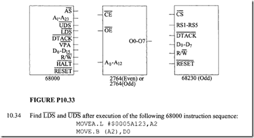
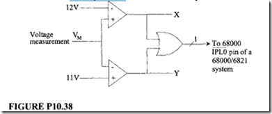
However, upon assertion of DTACK, the 68000 negates the AS, UDS, and LDS signals, and latches the data from the data bus into an internal register at the end of the next cycle. Once the selected peripheral device senses that the 68000 has obtained data from the data bus (by recognizing the negation of AS, UDS, or LDS ), the peripheral device must negate DTACK immediately so that it D0es not interfere with the start of the next cycle.

If DTACK is not asserted by the peripheral at the end of S4 (Figure I 0.13, SLOW READ), the 68000 inserts wait states. The 68000 outputs valid addresses on the address pins and keeps asserting AS, UDS, and LDS until the peripheral asserts DTACK. The 68000 always inserts an even number of wait states if DTACK is not asserted by the peripheral because all 68000 operations are performed using the clock with two states per clock cycle. Note in Figure 10.13 that the 68000 inserts 4 wait states or 2 cycles.

As an example of word read, consider that the 68000 is ready to execute the MOVE .W $ 6 0 212 2 , D0 instruction. The 68000 performs as follows:

1. At the end of S0 the 68000 places the upper 23 bits of the address 602122 16 on A3-A23·

2. At the end of SI, the 68000 asserts AS, UDS, and LDS.

image

image

3. The 68000 continues to output a HIGH on the RIW pin from the beginning of the read cycle to indicate a READ operation.

4. At the end of SO, the 68000 places appropriate outputs on the FC2-FCO pins to indicate either supervisor or user read.

5. If the peripheral asserts DTACK at the end of S4, the 68000 reads the contents of 602122 16 and 602123 16 via the Ds-D 15 and D0-D7 pins, respectively, into the high and low bytes ofD0.W at the end ofS6. If the peripheral D0es not assert DTACK at the end of S4, the 68000 continues to insert wait states.

Figure 10.14 shows a simplified timing diagram illustrating the use of DTACK for interfacing external memory and I/O chips to the 68000. As mentioned before, the 68000 checks the DTACK input pin at the falling edge of S4 (three cycles), the external memory, or I/O in this case, drives 68000 DTACK input to LOW, and the 68000 waits for one cycle and latches data at the end of S6. However, if the 68000 D0es not find DTACK LOW at the falling edge of S4, it waits for one clock cycle and then again checks DTACK for LOW. If DTACK is LOW, the 68000 latches data after one cycle (falling edge of S8). If the 68000 D0es not find DTACK LOW at the falling edge of S6, it checks for DTACK LOW at the falling edge of S8 and the process continues. Note that the minimum time to latch data is four cycles. This means that in the preceding example, if the 68000 clock frequency is 8 MHz, data will be latched after 500 ns because the DTACK is asserted LOW at the end ofS4 (375 ns).


68000 pins and signals , synchronous and asynchronous control lines , interrupt control lines , dma control lines and status lines

10.8 68000 Pins And Signals

The 68000 is usually packaged in one of the following:

a) 64-pin dual in-line package (DIP)

b) 68-pin quad pack

c) 68-terrninal chip carrier

d) 68-pin grid array (PGA)

Figure 10.6 shows the 68000 pin diagram for the DIP. Appendix C provides data sheets for the 68000 and support chips.

The 68000 is provided with two Vee (+5 V) and two ground pins. Power is thus distributed in order to reduce noise problems at high frequencies. Also, to build a prototype to demonstrate that the paper design for the 68000-based microcomputer is correct, one must use either wire-wrap or solder for the actual construction. Prototype board must not be used because, at high frequencies (above 4 MHz), there will be noise problems due to stray capacitances. The 68000 consumes about 1.5 W of power.

D0-D15 are the 16 data bus pins. All transfers to and from memory and I/O devices are conducted over the 8-bit (LOW or HIGH) or 16-bit data bus depending on the size of the device. A 1-A23 are the 23 address lines. A0 is obtained by encoding the UDS {upper data strobe) and LDS (lower data strobe) lines.

The 68000 operates on a single-phase TTL-level clock at 4, 6, 8, 10, 12.5, 16.67, or 25 MHz. The clock signal must be generated externally and applied to the 68000 clock input line. An external crystal oscillator chip is required to generate the clock. Figure I 0.7 shows the 68000 CLK waveform and clock timing specifications. The clock is at TTL­ compatible voltage. The clock timing specifications provide data for three different clock frequencies: 8 MHz, 10 MHz, and 12.5 MHz The 68000 CLK input can be provided by an external crystal oscillator or by designing an external circuit.

The 68000 signals can be divided into five functional categories:

image

image1. Synchronous and asynchronous control lines

2. System control lines

3. Interrupt control lines

4. DMA control lines

5. Status lines

10.8.1 Synchronous and Asynchronous Control Lines

The 68000 bus control is asynchronous. This means that once a bus cycle is initiated, the external device must send a signal back to complete it. The 68000 also contains three synchronous control lines that facilitate interfacing to synchronous peripheral devices such as Motorola’s inexpensive MC6800 family.

Synchronous operation means that bus control is synchronized or clocked using a common system clock signal. In 6800 family peripherals, this common clock is the E clock signal depending on the particular chip used. With synchronous control, all READ and WRITE operations must be synchronized with the common clock. However, this may create problems when interfacing with slow peripheral devices. This problem D0es not arise with asynchronous bus control.

Asynchronous operation is not dependent on a common clock signal. The 68000 utilizes the asynchronous control lines to transfer data between the 68000 and peripheral devices via handshaking. Using asynchronous operation, the 68000 can be interfaced to any peripheral chip regarD1ess of the speed.

The 68000 has three control lines to transfer data over its bus in a synchronous manner: E (enable), VPA (valid peripheral address), and VMA (valid memory address). The E clock corresponds to the clock of the 6800. The E clock is output at a frequency that is one tenth of the 68000 input clock. VPA is an input and tells the 68000 that a 6800 device is being addressed and therefore the data transfer must be synchronized with the E clock. VMA is the processor’s response to VPA. VMA is asserted when the memory address is valid. This also tells the external device that the next data transfer over the data bus will be synchronized with the E clock.

VPA can be generated by decoding the address pins and address strobe (AS). Note that the 68000 asserts AS LOW when the address on the address bus is valid. VMA is typically used as the chip select of the 6800 peripheral. This ensures that the 6800 peripherals are selected and deselected at the correct time. The 6800 peripheral interfacing sequence is as follows:

1. The 68000 initiates a cycle by starting a normal read or write cycle.

2. The 6800 peripheral defines the 68000 cycle by asserting the 68000 VPA input. If VPA is asserted as s00n as possible after assertion of AS, then VPA will be recognized as being asserted after three cycles. If VPA is not asserted after three cycles, the 68000 inserts wait states until VPA is recognized by the 68000 as asserted. DTACK should not be asserted while VPA is asserted. The 6800 peripheral must remove VPA within 1 clock period after AS is negated.

3. The 68000 monitors enable (E) until it is LOW. The 68000 then synchronizes all READ and WRITE operations with the E clock. The VMA output pin is asserted LOW by the 68000.

4. The 6800 peripheral waits until E is active (HIGH) and then transfers the data.

5. The 68000 waits until E goes to LOW (on a read cycle, the data is latched as E goes to LOW internally). The 68000 then negates VMA, AS, UDS, and LDS. The 68000 thus terminates the cycle and starts the next cycle.

The 68000 utilizes five lines to control address and data transfers asynchronously: AS(address strobe), R/W (read/write), DTACK (data acknowledge), UDS (upper data strobe), and LDS (lower data strobe).

The 68000 outputs to notify the peripheraJ device when data is to be transferred. AS is active LOW when the 68000 provides a valid address on the address bus. The R/W output line indicates whether the 68000 is reading data from or writing data into a peripheral device. RJW is HIGH for read and LOW for write. DTACK is used to tell the 68000 that a transfer is to be performed. When the 68000 wants to transfer data asynchronously, it first activates the AS line and at the same time generates the required address on the address lines to select the peripheral device.

Because the AS line tells the peripheral chip when to transfer data, the AS line should be part of the address decoding scheme. After enabling AS, the 68000 enters the wait state until it receives DTACK from the selected peripheral device. On receipt of DTACK, the 68000 knows that the peripheral device is ready for data transfer. The 68000 then utilizes the RJW and data lines to transfer data. UDS and LDS are defined as follows:

image

A0 is encoded from UDS and LDS. When UDS is asserted, the contents of even addresses are transferred on the high-order eight lines of the data bus, Ds-D15• The 68000 internally shifts this data to the low byte of the specified register. When LDS is asserted, the contents of odd addresses are transferred on the low-order eight lines of the data bus, D0– D7. During word and long word transfers, both UDS and LDS are asserted and information is transferred on all 16 data lines, D0-D15 pins. Note that during byte memory transfers, A0 correspo ds to UDS for even addresses (A0 = 0) and to LDS for odd addresses (A0 =1). The circuit in Figure 10.8 shows how even and odd addresses are interfaced to the 68000.

image

The 68000 has three control lines, BERR (bus error), HALT, and RESET, which are used to control system-related functions. BERR is an input to the 68000 and is used to inform the processor that there is a problem with the instruction cycle currently being executed. With asynchronous operation, this problem may arise if the 68000 D0es not receive DTACK from a peripheral device. An external timer can be used to activate the BERR pin if the external device D0es not send DTACK within a certain period of time. On receipt of BERR, the 68000 D0es one of the following:

  • Reruns the instruction cycle that caused the error.
  • Executes an error service routine.

The troubled instruction cycle is rerun by the 68000 if it receives a HALT signal along with the BERR signal. On receipt of LOW on both the HALT and BERR pins, the 68000 completes the current instruction cycle and then goes into the high-impedance state. On removal of both HALT and BERR (that is, when both HALT and BERR are HIGH), the 68000 reruns the troubled instruction cycle. The cycle can be rerun repeateD1y if both BERR and HALT are enabled/disabled continually.

On the other hand, an error service routine is executed only if the BERR signal is received without HALT. In this case, the 68000 will branch to a bus error vector address where the user can write a service routine. If two simultaneous bus. errors are received via the BERR pin without HALT, the 68000 automatically goes into the halt state until it is reset.

The HALT line can also be used by itself to perform single stepping or to provide DMA. When the HALT input is activated, the 68000 completes the current instruction and goes into a high-impedance state until HALT is returned to HIGH. By enabling/disabling the HALT line continually, the single-stepping debugging can be accomplished. However, because most 68000 instructions consist of more than one clock cycle, single stepping using HALT is not normally used. Rather, the trace bit in the status register is used to single-step the complete instruction.

One can also use HALT to perform microprocessor-halt DMA. Because the 68000 has separate DMA control lines, DMA using the HALT line will not normally be used. The HALT pin can also be used as an output signal. The 68000 will assert the HALT pin LOW when it goes into a halt state as a result of a catastrophic failure. The D0uble bus error (activation of BERR twice) is an example of this type of error. When this occurs, the 68000 goes into a high-impedance state until it is reset. The HALT line informs the peripheral devices of the catastrophic failure.

The RESET line of the 68000 is also bidirectional. To reset the 68000, both the RESET and HALT pins must be LOW for 10 clock cycles at the same time except when Vee is initially applied to the 68000. In this case, an external reset must be applied for at least 100 ms. The 68000 executes a reset service routine automatically for loading the PC with the starting address of the program.

The 68000 RESET pin can also be used as an output line. A LOW can be sent to this output line by executing the RESET instruction in the supervisor mode in order to reset external devices connected to the 68000 RESET pin. Upon execution of the RESET instruction, the 68000 drives the RESET pin LOW for 124 clock periods and D0es not affect any data, address, or status registers. Therefore, the RESET instruction can be placed anywhere in the program whenever the external devices need to be reset.

Upon hardware reset, the 68000 sets the S-bit in SR to 1, and then loads the supervisor stack pointer from location $000000 (high 16 bits) and $000002 (low 16 bits)

and loads the PC from $000004 (high 16 bits) and $000006 (low 16 bits); but the low 24 bits are used. In addition, the 68000 clears the trace bit in SR to 0 and sets bits 12 1110in SR to Ill. All other registers are unaffected.

10.8.3 Interrupt Control Lines

IPLO, IPLI, and IPL2 are the three interrupt control lines These lines provide for seven interrupt priority levels (IPL2, IPL I, IPLO = Ill means no interrupt, and IPL2, IPL I, IPLO

= 000 means nonmaskable interrupt with the highest priority). The 68000 interrupts will be discussed later in this chapter.

10.8.4 DMA Control Lines

The BR (bus request), BG (bus grant), and BGACK (bus grant acknowledge) lines are used for DMA purposes. The 68000 DMA will be discussed later in this chapter.

10.8.5 Status Lines

The 68000 has the three output lines called function code pins (output lines) FC2, FCI, and FCO. These lines tell external devices whether user data/program or supervisor data/ program is being addressed. These lines can be decoded to provide user or supervisor programs/data and interrupt acknowledge as shown in Table I 0.13.

The FC2, FC I, and FCO pins can be used to partition memory into four functional areas: user data memory, user program memory, supervisor data memory, and supervisor program memory. Each memory partition can directly access up to 16 megabytes, and thus the 68000 can be made to directly address up to 64 megabytes of memory. This is shown in Figure 10.9.


68000 pins and signals , synchronous and asynchronous control lines , system control lines , interrupt control lines , dma control lines and status lines

10.8 68000 Pins And Signals

The 68000 is usually packaged in one of the following:

a) 64-pin dual in-line package (DIP)

c) 68-terrninal chip carrier

b) 68-pin quad pack

d) 68-pin grid array (PGA)

Figure 10.6 shows the 68000 pin diagram for the DIP. Appendix C provides data sheets for the 68000 and support chips.

The 68000 is provided with two Vee (+5 V) and two ground pins. Power is thus distributed in order to reduce noise problems at high frequencies. Also, to build a prototype to demonstrate that the paper design for the 68000-based microcomputer is correct, one must use either wire-wrap or solder for the actual construction. Prototype board must not be used because, at high frequencies (above 4 MHz), there will be noise problems due to stray capacitances. The 68000 consumes about 1.5 W of power.

D0-D15 are the 16 data bus pins. All transfers to and from memory and I/O devices are conducted over the 8-bit (LOW or HIGH) or 16-bit data bus depending on the size of the device. A 1-A23 are the 23 address lines. A0 is obtained by encoding the UDS {upper data strobe) and LDS (lower data strobe) lines.

The 68000 operates on a single-phase TTL-level clock at 4, 6, 8, 10, 12.5, 16.67, or 25 MHz. The clock signal must be generated externally and applied to the 68000 clock input line. An external crystal oscillator chip is required to generate the clock. Figure I 0.7 shows the 68000 CLK waveform and clock timing specifications. The clock is at TTL­ compatible voltage. The clock timing specifications provide data for three different clock frequencies: 8 MHz, 10 MHz, and 12.5 MHz The 68000 CLK input can be provided by an external crystal oscillator or by designing an external circuit.

The 68000 signals can be divided into five functional categories:

image

image

1. Synchronous and asynchronous control lines

2. System control lines

3. Interrupt control lines

4. DMA control lines

5. Status lines

10.8.1 Synchronous and Asynchronous Control Lines

The 68000 bus control is asynchronous. This means that once a bus cycle is initiated, the external device must send a signal back to complete it. The 68000 also contains three synchronous control lines that facilitate interfacing to synchronous peripheral devices such as Motorola’s inexpensive MC6800 family.

Synchronous operation means that bus control is synchronized or clocked using a common system clock signal. In 6800 family peripherals, this common clock is the E clock signal depending on the particular chip used. With synchronous control, all READ and WRITE operations must be synchronized with the common clock. However, this may create problems when interfacing with slow peripheral devices. This problem D0es not arise with asynchronous bus control.

Asynchronous operation is not dependent on a common clock signal. The 68000 utilizes the asynchronous control lines to transfer data between the 68000 and peripheral devices via handshaking. Using asynchronous operation, the 68000 can be interfaced to any peripheral chip regarD1ess of the speed.

The 68000 has three control lines to transfer data over its bus in a synchronous manner: E (enable), VPA (valid peripheral address), and VMA (valid memory address). TheE clock corresponds to the clock of the 6800. TheE clock is output at a frequency that is one tenth of the 68000 input clock. VPA is an input and tells the 68000 that a 6800 device is being addressed and therefore the data transfer must be synchronized with the E clock. VMA is the processor’s response to VPA. VMA is asserted when the memory address is valid. This also tells the external device that the next data transfer over the data bus will be synchronized with the E clock.

VPA can be generated by decoding the address pins and address strobe (AS). Note that the 68000 asserts AS LOW when the address on the address bus is valid. VMA is typically used as the chip select of the 6800 peripheral. This ensures that the 6800 peripherals are selected and deselected at the correct time. The 6800 peripheral interfacing sequence is as follows:

I. The 68000 initiates a cycle by starting a normal read or write cycle.

2. The 6800 peripheral defines the 68000 cycle by asserting the 68000 VPA input.

If VPA is asserted as s00n as possible after assertion of AS, then VPA will be recognized as being asserted after three cycles. If VPA is not asserted after three cycles, the 68000 inserts wait states until VPA is recognized by the 68000 as asserted. DTACK should not be asserted while VPA is asserted. The 6800 peripheral must remove VPA within 1 clock period after AS is negated.

3. The 68000 monitors enable (E) until it is LOW. The 68000 then synchronizes all READ and WRITE operations with the E clock. The VMA output pin is asserted LOW by the 68000.

4. The 6800 peripheral waits until E is active (HIGH) and then transfers the data.

5. The 68000 waits until E goes to LOW (on a read cycle, the data is latched as E goes to LOW internally). The 68000 then negates VMA, AS, UDS, and LDS. The 68000 thus terminates the cycle and starts the next cycle.

The 68000 utilizes five lines to control address and data transfers asynchronously: AS(address strobe), R/W (read/write), DTACK (data acknowledge), UDS (upper data strobe), and LDS (lower data strobe).

The 68000 outputs to notify the peripheraJ device when data is to be transferred. AS is active LOW when the 68000 provides a valid address on the address bus. The R/W output line indicates whether the 68000 is reading data from or writing data into a peripheral device. RJW is HIGH for read and LOW for write. DTACK is used to tell the 68000 that a transfer is to be performed. When the 68000 wants to transfer data asynchronously, it first activates the AS line and at the same time generates the required address on the address lines to select the peripheral device.

Because the AS line tells the peripheral chip when to transfer data, the AS line should be part of the address decoding scheme. After enabling AS, the 68000 enters the wait state until it receives DTACK from the selected peripheral device. On receipt of DTACK, the 68000 knows that the peripheral device is ready for data transfer. The 68000 then utilizes the RJW and data lines to transfer data. UDS and LDS are defined as follows:

image

clip_image016A0 is encoded from UDS and LDS. When UDS is asserted, the contents of even addresses are transferred on the high-order eight lines of the data bus, Ds-D15• The 68000 internally shifts this data to the low byte of the specified register. When LDS is asserted, the contents of odd addresses are transferred on the low-order eight lines of the data bus, D0- D7. During word and long word transfers, both UDS and LDS are asserted and information is transferred on all 16 data lines, D0-D15 pins. Note that during byte memory transfers, A0 correspo ds to UDS for even addresses (A0 = 0) and to LDS for odd addresses (A0 =1). The circuit in Figure 10.8 shows how even and odd addresses are interfaced to the 68000.

image

10.8.2 System Control Lines

The 68000 has three control lines, BERR (bus error), HALT, and RESET, which are used to control system-related functions. BERR is an input to the 68000 and is used to inform the processor that there is a problem with the instruction cycle currently being executed. With asynchronous operation, this problem may arise if the 68000 Does not receive DTACK from a peripheral device. An external timer can be used to activate the BERR pin if the external device D0es not send DTACK within a certain period of time. On receipt ofBERR, the 68000 D0es one of the following:

  • Reruns the instruction cycle that caused the error.
  • Executes an error service routine.

The troubled instruction cycle is rerun by the 68000 if it receives a HALT signal along with the BERR signal. On receipt of LOW on both the HALT and BERR pins, the 68000 completes the current instruction cycle and then goes into the high-impedance state. On removal of both HALT and BERR (that is, when both HALT and BERR are HIGH), the 68000 reruns the troubled instruction cycle. The cycle can be rerun repeateD1y if both BERR and HALT are enabled/disabled continually.

On the other hand, an error service routine is executed only if the BERR signal is received without HALT. In this case, the 68000 will branch to a bus error vector address where the user can write a service routine. If two simultaneous bus. errors are received via the BERR pin without HALT, the 68000 automatically goes into the halt state until it is reset.

The HALT line can also be used by itself to perform single stepping or to provide DMA. When the HALT input is activated, the 68000 completes the current instruction and goes into a high-impedance state until HALT is returned to HIGH. By enabling/disabling the HALT line continually, the single-stepping debugging can be accomplished. However, because most 68000 instructions consist of more than one clock cycle, single stepping using HALT is not normally used. Rather, the trace bit in the status register is used to single-step the complete instruction.

One can also use HALT to perform microprocessor-halt DMA. Because the 68000 has separate DMA control lines, DMA using the HALT line will not normally be used. The HALT pin can also be used as an output signal. The 68000 will assert the HALT pin LOW when it goes into a halt state as a result of a catastrophic failure. The D0uble bus error (activation ofBERR twice) is an example of this type of error. When this occurs, the 68000 goes into a high-impedance state until it is reset. The HALT line informs the peripheral devices of the catastrophic failure.

The RESET line of the 68000 is also bidirectional. To reset the 68000, both the RESET and HALT pins must be LOW for 10 clock cycles at the same time except when Vee is initially applied to the 68000. In this case, an external reset must be applied for at least 100 ms. The 68000 executes a reset service routine automatically for loading the PC with the starting address of the program.

The 68000 RESET pin can also be used as an output line. A LOW can be sent to this output line by executing the RESET instruction in the supervisor mode in order to reset external devices connected to the 68000 RESET pin. Upon execution of the RESET instruction, the 68000 drives the RESET pin LOW for 124 clock periods and D0es not affect any data, address, or status registers. Therefore, the RESET instruction can be placed anywhere in the program whenever the external devices need to be reset.

Upon hardware reset, the 68000 sets the S-bit in SR to 1, and then loads the supervisor stack pointer from location $000000 (high 16 bits) and $000002 (low 16 bits) and loads the PC from $000004 (high 16 bits) and $000006 (low 16 bits); but the low 24 bits are used. In addition, the 68000 clears the trace bit in SR to 0 and sets bits 12 I I IO in SR to Ill. All other registers are unaffected.

10.8.3 Interrupt Control Lines

IPLO, IPLI, and IPL2 are the three interrupt control lines These lines provide for seven interrupt priority levels (IPL2, IPL I, IPLO = Ill means no interrupt, and IPL2, IPL I, IPLO = 000 means nonmaskable interrupt with the highest priority). The 68000 interrupts will be discussed later in this chapter.

10.8.4 DMA Control Lines

The BR (bus request), BG (bus grant), and BGACK (bus grant acknowledge) lines are used for DMA purposes. The 68000 DMA will be discussed later in this chapter.

10.8.5 Status Lines

The 68000 has the three output lines called function code pins (output lines) FC2, FCI, and FCO. These lines tell external devices whether user data/program or supervisor data/ program is being addressed. These lines can be decoded to provide user or supervisor programs/data and interrupt acknowledge as shown in Table I 0.13.

The FC2, FC I, and FCO pins can be used to partition memory into four functional areas: user data memory, user program memory, supervisor data memory, and supervisor program memory. Each memory partition can directly access up to 16 megabytes, and thus the 68000 can be made to directly address up to 64 megabytes of memory. This is shown in Figure 10.9.