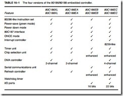
This section provides detail on the programming and operation of the 80186/80188 enhancements of all versions (XL, EA, EB, and EC). The next section details the use of the 80C188EB in a system that uses many of the enhancements discussed here. The only new feature not discussed here is the clock generator, which is described in the previous section on architecture.
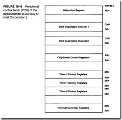
All internal peripherals are controlled by a set of 16-bit-wide registers located in the peripheral control block (PCB). The PCB (see Figure 16–6) is a set of 256 registers located in the I/O or memory space. Note that this set applies to the XL and EA versions. Later in this section, the EB and EC versions of the PCB are defined and described.
Whenever the 80186/80188 is reset, the peripheral control block is automatically located at the top of the I/O map (I/O addresses FF00H–FFFFH). In most cases, it stays in this area of I/O space, but the PCB may be relocated at any time to any other area of memory or I/O. Relocation is accomplished by changing the contents of the relocation register (see Figure 16–7) located at offset addresses FEH and FFH.
The relocation register is set to 20FFH when the 80186/80188 is reset. This locates the PCB at I/O addresses FF00H–FFFFH afterwards. To relocate the PCB, the user need only send a word OUT to I/O address FFFEH with a new bit pattern. For example, to relocate the PCB to


memory locations 20000H–200FFH, send 1200H to I/O address FFFEH. Notice that M>IO is a logic 1 to select memory, and that 200H selects memory address 20000H as the base address of the PCB. Note that all accesses to the PCB must be word accesses because it is organized as 16-bit-wide registers. Example 16–1 shows the software required to relocate the PCB to memory locations 20000H–200FFH. Note that either an 8- or 16-bit output can be used to program the 80186; in the 80188, never use the OUT DX,AX instruction because it takes additional clocking periods to execute.

The EB and EC versions use a different address for programming the PCB location. Both versions have the PCB relocation register stored at offset XXA8H, instead of at offset XXFEH for the XL and EA versions. The bit pattern of these versions is the same as for the XL and EA versions, except that the RMX bit is missing.
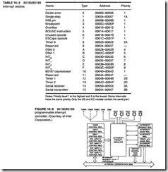
The interrupts in the 80186/80188 are identical to the 8086/8088, except that additional interrupt vectors are defined for some of the internal devices. A complete listing of the reserved interrupt vectors appears in Table 16–3. The first five are identical to the 8086/8088.
The array BOUND instruction interrupt is requested if the boundary of an index register is outside the values set up in the memory. The unused opcode interrupt occurs whenever the 80186/80188 executes any undefined opcode. This is important if a program begins to run awry. Note that the unused opcode interrupt can be accessed by an instruction, but the assembler does not include it in the instruction set. On the Pentium Pro–Pentium 4 and some earlier Intel micro- processors, the 0F0BH or 0FB9H instruction will cause the program to call the procedure whose address is stored at the unused opcode interrupt vector.
The ESC opcode interrupt occurs if ESC opcodes D8H–DFH are executed. This occurs only if the ET (escape trap) bit of the relocation register is set. If an ESC interrupt occurs, the address stored on the stack by the interrupt points to the ESC instruction or to its segment over- ride prefix, if one is used.
The internal hardware interrupts must be enabled by the I flag bit and must be unmasked to function. The I flag bit is set (enabled) with STI and cleared (disabled) with CLI. The remaining internally decoded interrupts are discussed with the timers and DMA controller, later in this section.
The interrupt controller inside the 80186/80188 is a sophisticated device. It has many interrupt inputs that arrive from the five external interrupt inputs, the DMA controller, and the three timers. Figure 16–8 provides a block diagram of the interrupt structure of the 80186/80188 interrupt

controller. This controller appears in the XL, EA, and EB versions, but the EC version contains the exact equivalent to a pair of 8259As, as found in Chapter 12. In the EB version, the DMA inputs are replaced with inputs from the serial unit for receive and transmit.
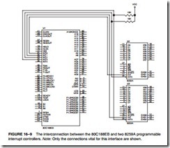
The interrupt controller operates in two modes: master and slave mode. The mode is selected by a bit in the interrupt control register (EB and EC versions) called the CAS bit. If the CAS bit is a logic 1, the interrupt controller connects to external 8259A programmable interrupt controllers (see Figure 16–9); if CAS is a logic 0, the internal interrupt controller is selected. In many cases, there are enough interrupts within the 80186/80188, so the slave mode is not

normally used. In the XL and EA versions, the master and slave modes are selected in the peripheral control register at offset address FEH.
This portion of the text does not detail the programming of the interrupt controller. Instead, it is limited to a discussion of the internal structure of the interrupt controller. The programming and application of the interrupt controller is discussed in the sections that describe the timer and DMA controller.
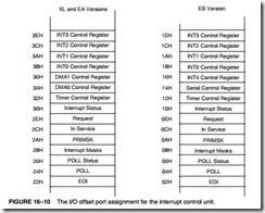
Interrupt Controller Registers. Figure 16–10 illustrates the interrupt controller’s registers. These registers are located in the peripheral control block beginning at offset address 22H. For the EC version, which is compatible with the 8259A, the interrupt controller ports are at offset addresses 00H and 02H for the master and ports 04H and 06H for the slave. In the EB version, the interrupt controller is programmed at offset address 02H. Note that the EB version has an additional interrupt input (INT4).
Slave Mode. When the interrupt controller operates in the slave mode, it uses up to two external 8259A programmable interrupt controllers for interrupt input expansion. Figure 16–9 shows how the external interrupt controllers connect to the 80186/80188 interrupt input pins for slave operation. Here, the INT0 and INT1 inputs are used as external connections to the interrupt request outputs of the 8259s, and INTA01INT22 and INTA11INT32 are used as interrupt acknowledge signals to the external controllers.
Interrupt Control Registers. There are interrupt control registers in both modes of operation, which each control a single interrupt source. Figure 16–11 depicts the binary bit pattern of each of these interrupt control registers. The mask bit enables (0) or disables (1) the interrupt input

represented by the control word, and the priority bits set the priority level of the interrupt source. The highest priority level is 000, and the lowest is 111. The CAS bit is used to enable slave or cascade mode (0 enables slave mode), and the SFNM bit selects the special fully nested mode. The SFNM allows the priority structure of the 8259A to be maintained.
Interrupt Request Register. The interrupt request register contains an image of the interrupt sources in each mode of operation. Whenever an interrupt is requested, the corresponding inter- rupt request bit becomes a logic 1, even if the interrupt is masked. The request is cleared when- ever the 80186/80188 acknowledges the interrupt. Figure 16–12 illustrates the binary bit pattern of the interrupt request register for both the master and slave modes.
Mask and Priority Mask Registers. The interrupt mask register has the same format as the interrupt register illustrated in Figure 16–12. If a source is masked (disabled), the corresponding bit of the interrupt mask register contains a logic 1; if enabled, it contains a logic 0. The interrupt mask register is read to determine which interrupt sources are masked and which are enabled. A source is masked by setting the source’s mask bit in its interrupt control register.
The priority mask register, illustrated in Figure 16–13, shows the priority of the interrupt currently being serviced by the 80186/80188. The level of the interrupt is indicated by priority bits P2–P0. Internally, these bits prevent an interrupt by a lower priority source. These bits are automatically set to the next lower level at the end of an interrupt, as issued by the 80186/80188.
In-Service Register. The in-service register has the same binary bit pattern as the request register of Figure 16–12. The bit that corresponds to the interrupt source is set if the 80186/80188 is currently acknowledging the interrupt. The bit is reset at the end of an interrupt.
The Poll and Poll Status Registers. Both the interrupt poll and interrupt poll status registers share the same binary bit patterns as those illustrated in Figure 16–14. These registers have a bit


(INT REQ) that indicates an interrupt is pending. This bit is set if an interrupt is received with sufficient priority, and cleared when an interrupt is acknowledged. The S bits indicate the interrupt vector type number of the highest priority pending interrupt.
The poll and poll status registers may appear to be identical because they contain the same information. However, they differ in function. When the interrupt poll register is read, the interrupt is acknowledged. When the interrupt poll status register is read, no acknowledge is sent. These registers are used only in the master mode, not in the slave mode.
End-of-Interrupt Register. The end-of-interrupt (EOI) register causes the termination of an interrupt when written by a program. Figure 16–15 shows the contents of the EOI register for both the master and slave mode.
In the master mode, writing to the EOI register ends either a specific interrupt level (vector number) or whatever level is currently active (nonspecific). In the nonspecific mode, the NSPEC bit must be set before the EOI register is written to end a nonspecific interrupt. The nonspecific EOI clears the highest level interrupt bit in the in-service register. The specific EOI clears the selected bit in the in-service register, which informs the microprocessor that the interrupt has been serviced and another interrupt of the same type can be accepted. The nonspecific mode is used unless there is a special circumstance that requires a different order for interrupt acknowl- edges. If a specific EOI is required, the vector number is placed in the EOI command. For example, to clear the timer 2 interrupt the EOI command is 13H (vector for timer 2).
In the slave mode, the level of the interrupt to be terminated is written to the EOI register. The slave mode does not allow a nonspecific EOI.
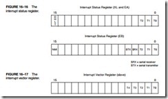
Interrupt Status Register. The format of interrupt status register is depicted in Figure 16–16. In the master mode, T2–T0 indicates which timer (timer 0, timer 1, or timer 2) is causing an inter- rupt. This is necessary because all three timers have the same interrupt priority level. These bits are set when the timer requests an interrupt and are cleared when the interrupt is acknowledged. The DHLT (DMA halt) bit is only used in the master mode; when set, it stops a DMA action. Note that the interrupt status register is different for the EB version.
Interrupt Vector Register. The interrupt vector register is present only in the slave mode, and only in the XL and EA versions at offset address 20H. It is used to specify the most significant five bits of the interrupt vector type number. Figure 16–17 illustrates the format of this register.
The 80186/80188 microprocessors contain three fully programmable 16-bit timers and each is totally independent of the others. Two of the timers (timer 0 and timer 1) have input and output

pins that allow them to count external events or generate wave-forms. The third timer (timer 2) connects to the 80186/80188 clock. Timer 2 is used as a DMA request source, as a prescalar for other timers, or as a watchdog timer.
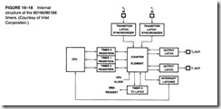
Figure 16–18 shows the internal structure of the timer unit. Notice that the timer unit contains one counting element that is responsible for updating all three counters. Each timer is actually a register that is rewritten from the counting element (a circuit that reads a value from a timer regis- ter and increments it before returning it). The counter element is also responsible for generating the outputs on the pins T0OUT and T1OUT, reading the T0IN and T1IN pins, and causing a DMA request
from the terminal count (TC) of timer 2 if timer 2 is programmed to request a DMA action.
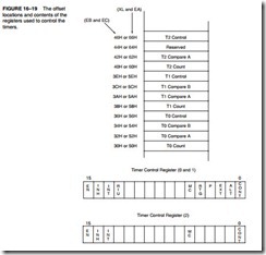
Timer Register Operation. The timers are controlled by a block of registers in the peripheral control block (see Figure 16–19). Each timer has a count register, maximum-count register or


registers, and a control register. These registers may all be read or written at any time because the 80186/80188 microprocessors ensure that the contents never change during a read or write.
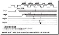
The timer count register contains a 16-bit number that is incremented whenever an input to the timer occurs. Timers 0 and 1 are incremented at the positive edge on an external input pin, every fourth 80186/80188 clock, or by the output of timer 2. Timer 2 is clocked on every fourth 80186/80188 clock pulse and has no other timing source. This means that in the 8 MHz version of the 80186/80188, timer 2 operates at 2 MHz, and the maximum counting frequency of timers 0 and 1 is 2 MHz. Figure 16–20 depicts these four clocking periods, which are not related to the bus timing.
Each timer has at least one maximum-count register, called a compare register (compare register A for timers 0 and 1), which is loaded with the maximum count of the count register to generate an output. Note that a timer is an up counter. Whenever the count register is equal to the maximum-count compare register, it is cleared to 0. With a maximum count of 0000H, the counter counts 65,536 times. For any other value, the timer counts the true value of the count. For example, if the maximum count is 0002H, the counter will count from 0 to 1 and then be cleared to 0—a modulus 2 counter has two states.

Timers 0 and 1 each have a second maximum-count compare register (compare register B) that is selected by the control register for the timer. Either maximum-count compare register A or both maximum-count compare registers A and B are used with these timers, as programmed by the ALT bit in the control register for the timer. When both maximum-count compare registers are used, the timer counts up to the value in maximum-count compare register A, clears to 0, and then counts up to the count in maximum-count compare register B. This process is then repeated. Using both maximum-count registers allows the timer to count up to 131,072.
The control register (refer to Figure 16–19) of each timer is 16 bits wide and specifies the operation of the timer. A definition of each control bit follows:
EN The enable bit allows the timer to start counting. If EN is cleared, the timer does not count; if it is set, the timer counts.
INH The inhibit bit allows a write to the timer control register to affect the enable bit (EN).
If INH is set, then the EN bit can be set or cleared to control the counting. If INH is cleared, EN is not affected by a write to the timer control register. This allows other features of the timer to be modified without enabling or disabling the timer.
INT The interrupt bit allows an interrupt to be generated by the timer. If INT is set, an interrupt will occur each time that the maximum count is reached in either maximum- count compare register. If this bit is cleared, no interrupt is generated. When the interrupt request is generated, it remains in force, even if the EN bit is cleared after the interrupt request.
RIU The register in use bit indicates which maximum-count, compare register is currently in use by the timer. If RIU is a logic 0, then maximum-count compare register A is in use. This bit is a read-only bit, and writes do not affect it.
MC The maximum count bit indicates that the timer has reached its maximum count.
This bit becomes a logic 1 when the timer reaches its maximum count and remains a logic 1 until the MC bit is cleared by writing a logic 0. This allows the maximum count to be detected by software.
RTG The retrigger bit is active only for external clocking (EXT = 0). The RTG bit is used only with timers 0 and 1 to select the operation of the timer input pins (T0IN and T1IN).
If RTG is a logic 0, the external input will cause the timer to count if it is a logic 1; the timer will hold its count (stop counting) if it is a logic 0. If RTG is a logic 1, the external input pin clears the timer count to 0000H each time a positive-edge occurs.
P The prescalar bit selects the clocking source for timers 0 and 1. If EXT = 0 and P = 0, the source is one fourth the system clock frequency. If P = 1, the source is timer 2.
EXT The external bit selects internal timing (EXT = 0) or external timing (EXT = 1). If EXT = 1, the timing source is applied to the T0IN or T1IN pins. In this mode, the timer increments after each positive-edge on the timer input pin. If EXT = 0, the clocking source is from one of the internal sources.
ALT The alternate bit selects single maximum-count mode (maximum-count compare register A) if a logic 0, or alternate maximum-count mode (maximum-count compare registers A and B) if a logic 1.
CONT The continuous bit selects continuous operation if a logic 1. In continuous operation, the counter automatically continues counting after it reaches its maximum count. If CONT is a logic 0, the timer will automatically stop counting and clear the EN bit. Note that whenever the 80186/80188 are reset, the timers are automatically disabled.
Timer Output Pin. Timers 0 and 1 have an output pin used to generate either square waves or pulses. To produce pulses, the timer is operated in single maximum-count mode (ALT = 0). In this mode, the output pin goes low for one clock period when the counter reaches its maximum count. By controlling the CONT bit in the control register, either a single pulse or continuous pulses can be generated.
To produce square waves or varying duty cycles, the alternate mode (ALT = 1) is selected. In this mode, the output pin is a logic 1 while maximum-count compare register A controls the timer; it is a logic 0 while maximum-count compare register B controls the timer. As with the single maximum-count mode, the timer can generate either a single square wave or continuous square waves. See Table 16–4 for the function of the ALT and CONT control bits.
Almost any duty cycle can be generated in the alternate mode. For example, suppose that a 10% duty cycle is required at a timer output pin. Maximum-count register A is loaded with a 10 and maximum-count register B is loaded with a 90 to produce an output that is a logic 1 for 10 clocks and a logic 0 for 90 clocks. This also divides the frequency of the timing source by a factor of 100.
Real-Time Clock Example. Many systems require the time of day. This is often called a real- time clock (RTC). A timer within the 80186/80188 can provide the timing source for software that maintains the time of day.
The hardware required for this application is not illustrated because all that is required is that the T1IN pin must be connected to +5.0 V through a pull-up resistor to enable timer 1. In the
example, timers 1 and 2 are used to generate a one-second interrupt that provides the software
with a timing source.
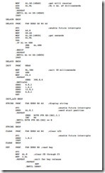
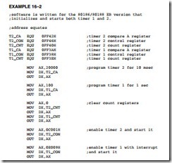
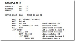
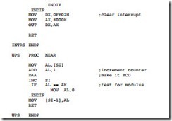
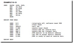
The software required to implement a real-time clock is listed in Examples 16–2 and 16–3. Example 16–2 illustrates the software required to initialize the timers. Example 16–3 shows an interrupt service procedure, which keeps time. There is another procedure in Example 16–3 that increments a BCD modulus counter. None of the software required to install the interrupt vector and set or display time of day is illustrated here.


Timer 2 is programmed to divide by a factor of 20,000. This causes the clock (assuming a 2 MHz on the 8 MHz version of the 80186/80188) to be divided down to one pulse every 10 ms. The clock for timer 1 is derived internally from the timer 2 output. Timer 1 is programmed to divide the Timer 2 clock by 100 and generate a pulse once per second. The control register of timer 1 is programmed so that the one-second pulse internally generates an interrupt.
The interrupt service procedure is called once per second to keep time. The interrupt service procedure adds a one to the content of memory location SECONDS on each interrupt. Once every 60 seconds, the content of the next memory location (SECONDS + 1) is incremented. Finally, once per hour, the content of memory location SECONDS + 2 is incremented. The time is stored in these three consecutive memory locations in BCD, so the system software can easily access the time.


The DMA controller within the 80186/80188 has two fully independent DMA channels. Each has its own set of 20-bit address registers, so any memory or I/O location is accessible for a DMA transfer. In addition, each channel is programmable for auto-increment or auto-decrement to either source or destination registers. This controller is not available in the EB or EC versions. The EC version contains a modified four-channel DMA controller; the EB version contains no DMA controller. This text does not describe the DMA controller within the EC version.
Figure 16–21 illustrates the internal register structure of the DMA controller. These registers are located in the peripheral control block at offset addresses C0H–DFH.

Notice that both DMA channel register sets are identical; each channel contains a control word, a source and destination pointer, and a transfer count. The transfer count is 16 bits wide and allows unattended DMA transfers of bytes (80188/80186) and words (80186 only). Each time that a byte or word is transferred, the count is decremented by one until it reaches 0000H—the terminal count.
The source and destination pointers are each 20 bits wide, so DMA transfers can occur to any memory location or I/O address without concern for segment and offset addresses. If the source or destination address is an I/O port, bits A19–A16 must be 0000 or a malfunction may occur.
Channel Control Register. Each DMA channel contains its own channel control register (refer to Figure 16–21), which defines its operation. The leftmost six bits specify the operation of the source and destination registers. The M>IO bit indicates a memory or I/O location, DEC causes the pointer to be decremented, and INC causes the pointer to be incremented. If both the INC and DEC bits are 1, then the pointer is unchanged after each DMA transfer. Notice that memory-to- memory transfers are possible with this DMA controller.
The TC (terminal count) bit causes the DMA channel to stop transfers when the channel count register is decremented to 0000H. If this bit is a logic 1, the DMA controller continues to transfer data, even after the terminal count is reached.
The INT bit enables interrupts to the interrupt controller. If set, the INT bit causes an inter- rupt to be issued when the terminal count of the channel is reached.
The SYN bit selects the type of synchronization for the channel: 00 = no synchronization, 01 = source synchronization, and 10 = destination synchronization. When either unsynchronized or source synchronization is selected, data are transferred at the rate of 2M bytes per second. These two types of synchronization allow transfers to occur without interruption. If destination synchronization is selected, the transfer rate is slower (1.3M bytes per second), and the controller relinquishes control to the 80186/80188 after each DMA transfer.
The P bit selects the channel priority. If P = 1, the channel has the highest priority. If both channels have the same priority, the controller alternates transfers between channels.
The TRDQ bit enables DMA transfers from timer 2. If this bit is a logic 1, the DMA request originates from timer 2. This can prevent the DMA transfers from using all of the micro- processor’s time for the transfer.
The CHG>NOCHG bit determines whether START>STOP changes for a write to the con-
trol register. The START>STOP bit starts or stops the DMA transfer. To start a DMA transfer, both CHG>NOCHG and START>STOP are placed at a logic 1 level.
The BYTE>WORD selects whether the transfer is byte- or word-sized.
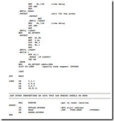
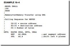
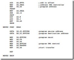
Sample Memory-to-Memory Transfer. The built-in DMA controller is capable of performing memory-to-memory transfers. The procedure used to program the controller and start the trans- fer is listed in Example 16–4.


The procedure in Example 16–4 transfers data from the data segment location addressed by SI into the extra segment location addressed by DI. The number of bytes transferred is held in register CX. This operation is identical to the REP MOVSB instruction, but execution occurs at a much higher speed through the use of the DMA controller.
The chip selection unit simplifies the interface of memory and I/O to the 80186/80188. This unit contains programmable chip selection logic. In small- and medium-sized systems, no external decoder is required to select memory and I/O. Large systems, however, may still require external decoders. There are two forms of the chip selection unit; one form found in the XL and EA versions differs from the unit found in the EB and EC versions.
Memory Chip Selects. Six pins (XL and EA versions) or 10 pins (EB and EC versions) are used to select different external memory components in a small- or medium-sized 80186/80188-based system. The UCS (upper chip select) pin enables the memory device located in the upper portion of the memory map that is most often populated with ROM. This programmable pin allows the size of the ROM to be specified and the number of wait states required. Note that the ending address of the ROM is FFFFFH. The LCS (lower chip select) pin selects the memory device (usually a RAM) that begins at memory location 00000H. As with the UCS pin, the memory size and number of wait states are programmable. The remaining four or eight chip select pins select middle memory devices. The four pins in the XL and EA version 1MCS3 – MCS02 are programmed for both the starting (base) address and memory size. Note that all devices must be of the same size. The eight pins 1GCS7 – GCS02 in the EB and EC versions are programmed by size and also by starting address. These selection signals represent a memory device or an I/O device.
Peripheral Chip Selects. The 80186/80188 addresses up to seven external peripheral devices with pins PCS6 – PCS0 (in the XL and EA versions). The GCS pins are used in the EB and EC versions to select up to eight memory or I/O devices. The base I/O address is programmed at any 1K- byte interval with port address block sizes of 128 bytes (64 bytes on the EB and EC versions).

Programming the Chip Selection Unit for XL and EA Versions. The number of wait states in each section of the memory and the I/O are programmable. The 80186/80188 microprocessors have a built-in wait state generator that can introduce between 0 and 3 wait states (XL and EA version). Table 16–5 lists the logic levels required on bits R2–R0 in each programmable register to select various numbers of wait states. These three lines also select if an external READY signal is required to generate wait states. If READY is selected, the external READY signal is in parallel with the internal wait state generator. For example, if READY is a logic 0 for three clocking periods but the internal wait state generator is programmed to insert two wait states, three wait states are inserted.
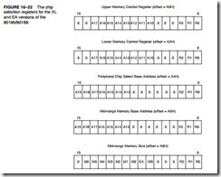
Suppose that a 64K-byte EPROM is located at the top of the memory system and requires two wait states for proper operation. To select this device for this section of memory, the UCS pin is programmed for a memory range of F0000H–FFFFFH with two wait states. Figure 16–22


lists the control registers for all memory and I/O selections in the peripheral control block at off- set addresses A0–A9H. Notice that the rightmost three bits of these control registers are from Table 16–5. The control register for the upper memory area is at location PCB offset address A0H. This 16-bit register is programmed with the starting address of the memory area (F0000H, in this case) and the number of wait states. Please note that the upper two bits of the address must be programmed as 00, and that only address bits A17–A10 are programmed into the control regis- ter. See Table 16–6 for examples illustrating the codes for various memory sizes. Because our example requires two wait states, the basic address is the same as in the table for a 64K device, except that the rightmost three bits are 110 instead of 100. The datum sent to the upper memory control register is 3006H.
Suppose that a 32K-byte SRAM that requires no waits and no READY input is located at the bottom of the memory system. To program the LCS pin to select this device, register A2 is loaded in exactly the same manner as register A0H. In this example, a 07FCH is sent to register A2H. Table 16–7 lists the programming values for the lower chip-selection output.
The central part of the memory is programmed via two registers: A6H and A8H. Register A6H programs the beginning or base address of the middle memory select lines 1MCS3 – MCS02 and number of waits. Register A8H defines the size of the block of memory and the individual memory device size (see Table 16–8). In addition to block size, the number of peripheral wait states are programmed as with other areas of memory. The EX (bit 7) and MS (bit 6) specify the peripheral selection lines, and will be discussed shortly.
For example, suppose that four 32K-byte SRAMs are added to the middle memory area, beginning at location 80000H and ending at location 9FFFFH with no wait states. To program the middle memory selection lines for this area of memory, we place the leftmost seven address bits in


register A6H, with bits 8–3 containing logic 0s, and the rightmost three bits containing the ready control bits. For this example, register A6H is loaded with 8004H. Register A8H is programmed with 1F44H, assuming that EX = 0 and MS = 1 and no wait states and no READY are required for the peripherals.
Register A4H programs the peripheral chip selection pins 1PCS6 – PCS02 along with the EX and MS bits of register A8H. Register A4H holds the beginning or base address of the peripheral selection lines. The peripherals may be placed in memory or in the I/O map. If they are placed in the I/O map, A19–A16 of the port number must be 0000. Once the starting address is programmed on any 1K-byte I/O address boundary, the PCS pins are spaced at 128-byte intervals.
For example, if register A4H is programmed with a 0204H, with no waits and no READY synchronization, the memory address begins at 02000H or the I/O port begins at 2000H. In this case, the I/O ports are: PCS0 = 2000H, PCS1 = 2080H, PCS2 = 2100H, PCS3 = 2180H, PCS4 = 2200H, PCS5 = 2280H, and PCS5 = 2300H.
The MS bit of register A8H selects memory mapping or I/O mapping for the peripheral select pins. If MS is a logic 0, then the PCS lines are decoded in the memory map; if it is a logic 1, then the PCS lines are in the I/O map.
The EX bit selects the function of the PCS5 and PCS6 pins. If EX = 1, these PCS pins select I/O devices; if EX = 0, these pins provide the system with latched address lines A1 and A2. The A1 and A2 pins are used by some I/O devices to select internal registers and are provided for this purpose.
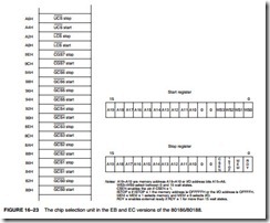
Programming the Chip Selection Unit for EB and EC Versions. As mentioned earlier, the EB and EC versions have a different chip selection unit. These newer versions of the 80186/80188 contain an upper and lower memory chip selection pin as do earlier versions, but they do not contain middle selection and peripheral selection pins. In place of the middle and peripheral chip selection pins, the EB and EC versions contain eight general chip selection pins 1GCS7 – GCS02 that select either a memory device or an I/O device.
Programming is also different because each of the chip selection pins contains a starting address register and an ending address register. See Figure 16–23 for the offset address of each pin and the contents of the start and end registers.
Notice that programming for the EB and EC versions of the 80186/80188 is much easier than for the earlier XL and EA versions. For example, to program the UCS pin for an address that begins at location F0000H and ends at location FFFFFH (64K bytes), the starting address register (offset = A4H) is programmed with F002H for a starting address of F0000H with two wait states. The ending address register (offset = A6H) is programmed with 000EH for an ending address of FFFFFH for memory with no external ready synchronization. The other chip selection pins are programmed in a similar fashion.
