THE UNIVERSAL SERIAL BUS (USB)
The universal serial bus (USB) has solved a problem with the personal computer system. The current PCI sound cards use the internal PC power supply, which generates a tremendous amount of noise. Because the USB allows the sound card to have its own power supply, the noise associated with the PC power supply can be eliminated, allowing for high-fidelity sound without 60 Hz hum. Other benefits are ease of user connection and access to up to 127 different connections through a four-connection serial cable. This interface is ideal for keyboards, sound cards, simple video-retrieval devices, and modems. Data transfer speeds are 480 Mbps for full-speed USB 2.0 operation, 11 Mbps for USB 1.1 compliant transfers, and 1.5 Mbps for slow-speed operation.
Cable lengths are limited to five meters maximum for the full-speed interface and three meters maximum for the low-speed interface. The maximum power available through these cables is rated at 100 mA and maximum current at 5.0 V. If the amount of current exceeds 100 mA, Windows will display a yellow exclamation point next to the device, indicating an overload condition.
The Connector
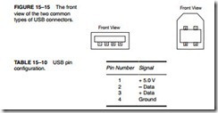
Figure 15–15 illustrates the pin-out of the USB connector. There are two types of connectors specified and both are in use. In either case, there are four pins on each connector, which contain the signals indicated in Table 15–10. As mentioned, the +5.0 V and ground signals can be used to power devices connected to the bus as long as the amount of current does not exceed 100 mA per device. The data signals are biphase signals. When +data are at 5.0 V, -data are at zero volts and vice versa.
USB Data
The data signals are biphase signals that are generated using a circuit such as the one illustrated in Figure 15–16. The line receiver is also illustrated in Figure 15–16. Placed on the transmission pair is a noise-suppression circuit that is available from Texas Instruments (SN75240). Once the
transceiver is in place, interfacing to the USB is complete. The 75773 integrated circuit from Texas Instruments functions as both the differential line driver and receiver for this schematic.
The next phase is learning how the signals interact on the USB. These signals allow data to be sent and received from the host computer system. The USB uses NRZI (non-return to zero, inverted) data encoding for transmitting packets. This encoding method does not change the signal level for the transmission of a logic 1, but the signal level is inverted for each change to a logic 0. Figure 15–17 illustrates a digital data stream and the USB signal produced using this encoding method.
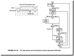
The actual data transmitted includes sync bits using a method called bit stuffing. If a logic 1 is transmitted for more than 6 bits in a row, the bit stuffing technique adds an extra bit (logic 0) after six continuous 1s in a row. Because this lengthens the data stream, it is called bit stuffing. Figure 15–18 shows a bit-stuffed serial data stream and the algorithm used to create it from raw digital serial data. Bit stuffing ensures that the receiver can maintain synchronization for long strings of 1s. Data are always transmitted beginning with the least-significant bit first, followed by subsequent bits.
USB Commands
Now that the USB data format is understood, we will discuss the commands used to transfer data and select the receptor. To begin communications, the sync byte (80H) is transmitted first, fol- lowed by the packet identification byte (PID). The PID contains 8 bits, but only the rightmost 4 bits contain the type of packet that follows, if any. The leftmost 4 bits of the PID are the ones complementing the rightmost 4 bits. For example, if a command of 1000 is sent, the actual byte sent for the PID is 0111 1000. Table 15–11 shows the available 4-bit PIDs and their 8-bit codes. Notice that PIDs are used as token indicators, as data indicators, and for handshaking.
Figure 15–19 lists the formats of the data, token, handshaking, and start-of-frame packets found on the USB. In the token packet, the ADDR (address field) contains the 7-bit address of the USB device. As mentioned earlier, there are up to 127 devices present on the USB at a time. The ENDP (endpoint) is a 4-bit number used by the USB. Endpoint 0000 is used for initialization; other endpoint numbers are unique to each USB device.
There are two types of CRC (cyclic redundancy checks) used on the USB: One is a 5-bit CRC and the other (used for data packets) is a 16-bit CRC. The 5-bit CRC is generated with the X5 + X2 + 1 polynomial; the 16-bit CRC is generated with the X16 + X15 + X2 + 1 polynomial.
When constructing circuitry to generate or detect the CRC, the plus signs represent Exclusive-
OR circuits. The CRC circuit or program is a serial checking mechanism. When using the 5-bit CRC, a residual of 01100 is received for no error in all five bits of the CRC and the data bits. With the 16-bit CRC, the residual is 1000000000001101 for no error.
token back to the host. If the data and CRC are received correctly, the ACK is sent; if not, the NAK is sent. If the host receives a NAK token, it retransmits the data packet until the receiver finally receives it correctly. This method of data transfer is often called stop and wait flow control. The host must wait for the client to send an ACK or NAK before transferring additional data packets.
The USB Bus Node
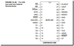
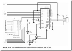
National Semiconductor produces a USB bus interface that is fairly easy to interface to the micro- processor. Figure 15–20 illustrates the USBN9604 USB node. Connecting this device to a system using non-DMA access is accomplished by connecting the data bus to D0–D7, the control inputs RD, WR, and CS, and a 24 MHz fundamental crystal across the XIn and XOut pins. The USB bus connection is located on the D- and D+ pins. The simplest interface is achieved by connecting the two mode inputs to ground. This places the device into a nonmultiplexed parallel mode. In this mode the A0 pin is used to select address (1) or data (0). Figure 15–21 shows this connection to the microprocessor decodes at I/O port addresses 0300H (data) and 0301H (address).
The USBN9604 is a USB bus transceiver that can receive USB data and transmit USB data. This provides an interface point to the USB bus for a minimal cost of about two dollars.
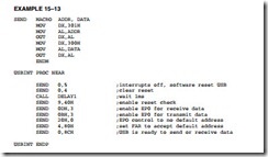
The software presented here functions with the interface in Figure 15–21. Not provided is the driver software for the host system. Example 15–13 illustrates the code required to initialize the USB controller. The USBINT procedure sets the USB controller to use end point zero for data transfers.
Once the USB controller is initialized, data can be sent or received to the host system through the USB. To accomplish data transmission, the procedure illustrated in Example 15–14 is called to send a 1-byte packet using the TXD0 FIFO. This procedure uses the SEND macro listed in Example 15–13 to transfer the byte in BL through the USB to the host system.
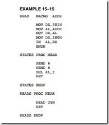
To receive data from the USB, two functions are required. One tests to see if data are avail- able and the other reads a byte from the USB and places it into the BL register. Both procedures are listed in Example 15–15. The STATUS procedure checks to see if data are in the receiver FIFO. If data are present, carry is set upon return and if no data are received, carry is cleared. The READS procedure retrieves a byte for the receiver FIFO and returns it in BL.
