SPECIAL 80386 REGISTERS
A new series of registers, not found in earlier Intel microprocessors, appears in the 80386 as control, debug, and test registers. Control registers CR0–CR3 control various features, DR0–DR7 facilitate debugging, and registers TR6 and TR7 are used to test paging and caching.
Control Registers
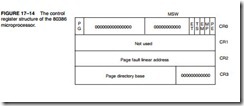
In addition to the EFLAGS and EIP as described earlier, there are other control registers found in the 80386. Control register 0 (CR0) is identical to the MSW (machine status word) found in the 80286 microprocessor, except that it is 32 bits wide instead of 16 bits wide. Additional control registers are CR1, CR2, and CR3.
Figure 17–14 illustrates the control register structure of the 80386. Control register CR1 is not used in the 80386, but is reserved for future products. Control register CR2 holds the linear page address of the last page accessed before a page fault interrupt. Finally, control register CR3 holds the base address of the page directory. The rightmost 12 bits of the 32-bit page table address contain zeros and combine with the remainder of the register to locate the start of the 4K- long page table.
Register CR0 contains a number of special control bits that are defined as follows in the 80386:
PG Selects page table translation of linear addresses into physical addresses when PG = 1. Page table translation allows any linear address to be assigned any physical memory location.
ET Selects the 80287 coprocessor when ET 0 or the 80387 coprocessor when ET l.
This bit was installed because there was no 80387 available when the 80386 first appeared. In most systems, ET is set to indicate that an 80387 is present in the system.
TS Indicates that the 80386 has switched tasks (in protected mode, changing the con- tents of TR places a 1 into TS). If TS 1, a numeric coprocessor instruction causes a type 7 (coprocessor not available) interrupt.
EM The emulate bit is set to cause a type 7 interrupt for each ESC instruction. (ESCape instructions are used to encode instructions for the 80387 coprocessor.) Once this feature was used to emulate interrupts with software, the function of the coprocessor. Emulation reduces the system cost, but it often requires at least 100 times longer to execute the emulated coprocessor instructions.
MP Is set to indicate that the arithmetic coprocessor is present in the system.
PE Is set to select the protected mode of operation for the 80386. It may also be cleared to reenter the real mode. This bit can only be set in the 80286. The 80286 could not return to real mode without a hardware reset, which precludes its use in most systems that use protected mode.
Debug and Test Registers
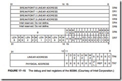
Figure 17–15 shows the sets of debug and test registers. The first four debug registers contain 32- bit linear breakpoint addresses. (A linear address is a 32-bit address generated by a microprocessor instruction that may or may not be the same as the physical address.) The breakpoint addresses, which may locate an instruction or datum, are constantly compared with the addresses generated by the program. If a match occurs, the 80386 will cause a type 1 interrupt (TRAP or
debug interrupt) to occur, if directed by debug registers DR6 and DR7. This feature is a much- expanded version of the basic trapping or tracing allowed with the earlier Intel microprocessors through the type 1 interrupt. The breakpoint addresses are very useful in debugging faulty soft- ware. The control bits in DR6 and DR7 are defined as follows:
BT If set (1), the debug interrupt was caused by a task switch.
BS If set, the debug interrupt was caused by the TF bit in the flag register.
BD If set, the debug interrupt was caused by an attempt to read the debug register with the GD bit set. The GD bit protects access to the debug registers.
B3–B0 Indicate which of the four debug breakpoint addresses caused the debug interrupt.
LEN Each of the four length fields pertains to each of the four breakpoint addresses
stored in DR0–DR3. These bits further define the size of access at the breakpoint address as 00 (byte), 01 (word), or 11 (doubleword).
RW Each of the four read/write fields pertains to each of the four breakpoint addresses stored in DR0–DR3. The RW field selects the cause of action that enabled a break- point address as 00 (instruction access), 01 (data write), and 11 (data read and write).
GD If set, GD prevents any read or write of a debug register by generating the debug interrupt. This bit is automatically cleared during the debug interrupt so that the debug registers can be read or changed, if needed.
GE If set, selects a global breakpoint address for any of the four breakpoint address registers.
LE If set, selects a local breakpoint address for any of the four breakpoint address registers.
The test registers, TR6 and TR7, are used to test the translation look-aside buffer (TLB). The TLB is used with the paging unit within the 80386. The TLB, which holds the most com- monly used page table address translations, reduces the number of memory reads required for looking up page translation addresses in the page translation tables. The TLB holds the most common 32 entries from the page table, and it is tested with the TR6 and TR7 test registers.
Test register TR6 holds the tag field (linear address) of the TLB, and TR7 holds the physi- cal address of the TLB. To write a TLB entry, perform the following steps:
1. Write TR7 for the desired physical address, PL, and REP values.
2. Write TR6 with the linear address, making sure that C = 0.
To read a TLB entry:
1. Write TR6 with the linear address, making sure that C = 1.
2. Read both TR6 and TR7. If the PL bit indicates a hit, then the desired values of TR6 and TR7
indicate the contents of the TLB.
The bits found in TR6 and TR7 indicate the following conditions:
V Shows that the entry in the TLB is valid.
D Indicates that the entry in the TLB is invalid or dirty.
U A bit for the TLB.
W Indicates that the area addressed by the TLB entry is writable.
C Selects a write (0) or immediate lookup (1) for the TLB.
PL Indicates a hit if a logic 1.
REP Selects which block of the TLB is written.
Refer to the section on memory management and the paging unit for more detail on the function of the TLB.

