Effectively Optimizing Combinatorial Circuits
In the first chapter, I introduced you to the basic theory behind digital electronics: binary data is manipulated by six different simple operations. With this knowledge, you actually have enough information to be able to design very complex operations, taking a number of different bits as input. The problem with these circuits is that they will probably not be ‘‘optimized’’ in order to minimize the number of gates, the speed which the digital electronic circuit responds to the inputs and finally, whether or not the circuit is optimized for the technology that it will be implemented in.
These three parameters are the basic measurements used to determine whether or not a circuit is effectively optimized. The number of gates should be an obvious one and you should realize that the more gates, the higher the chip count and cost of implementing the circuit as well as the increased complexity in wiring it. Right now, connections between logic gates are just black lines on paper to you – but when you start trying to wire circuits that you have designed, you will discover first hand that simplifying the wiring of a circuit often reduces costs more than reducing the number of chips would indicate. Small improvements in the complexity of a circuit can have surprising cost ramifications when you look at the overall cost of the application. You may find that eliminating 1% of the gates in an application will result in as much as a 10–20% overall reductions in product cost. These savings are a result of being able to build the circuit on a smaller PCB or one which requires fewer layers (which can reduce the overall product cost dramatically). If the application is going to use a programmable logic technology, you may find that with the optimized circuit, lower cost chips can be substituted into the design. Fewer gates in an application also results in less power being dissipated by the circuit, requiring less cooling and a smaller power supply.
The speed that signals pass through gates is not infinite; standard TTL requires 8 billionths of a second (called a ‘‘nanosecond’’ and uses the abbreviation ‘‘ns’’) to pass a signal through a ‘‘NAND’’ gate. The term given to this time is known as the ‘‘gate delay’’. Halving the number of gates a signal has to pass through (which is halving the number of gate delays) will double the speed in which it can respond to a changing input. As you work with more complex circuits, you will discover that you will often have to optimize a circuit for speed or else you may have to use a faster (and generally more expensive) technology.
The last parameter, what I call ‘‘technology optimization’’, on the surface may seem more intangible than the other two parameters as well as have its measurements use the other two parameters, but when working with physical devices, it is the most important factor in properly optimizing your application. Before moving on and considering your circuit ‘‘done’’, you should look at how it will actually be implemented in the technology that you are using and look for optimizations that will reduce the actual number of gates and gate delays required by the application.
You can consider logic optimization to be a recursive operation, repeatedly optimizing all the different parameters and measurements. Once you have specified the required logic functions, you should look at how it will be implemented in the actual circuit. Once you have converted it to the actual circuit, you will then go back and look for opportunities for decreasing the number of gates, speeding up the time the signal passes through the gates and again look for technology optimizations. This will continue until you are satisfied with the final result.
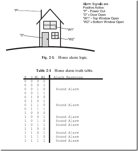
To illustrate what I mean, in this chapter, I will look at a practical example, a simple home burglar alarm. In Fig. 2-1, I have drawn a very basic house, which has two windows, a door and power running to it. Sensors, on
the windows, door and power are passed to an alarm system. When the alarm system was designed a table of the different possible combinations of inputs was generated (Table 2-1), with the combinations that would cause the alarm to sound indicated. As I have noted in Fig. 2-1, the alarm inputs are positive active, which means I can represent them as being active with a ‘‘1’’.
In this fictional house, I assumed that the upper window (‘‘W1’’) should never be opened – if it were opened, then the alarm would sound. Along with this, I decided that if the power failed and either of the windows were opened, then the alarm failed; this would be the case where the power to the house was cut and somebody forced open the window. Table 2-1 shows the cases where the alarm should sound and you will notice that the cases where the alarm should sound are either a single event in the table, or a case where three are grouped together.
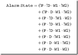
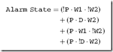
After building the table, you should also create a sum of products equation for the function:
You could also draw a logic diagram using the gate symbols that I introduced in the first chapter. I found that this diagram was very complex and very difficult to follow. If you were to try it yourself, you would discover that the logic diagram would consist of 12 NOTs, 24 two input ANDs (knowing that a single four input AND can be produced from three two input ANDs) and seven two input OR gates with the maximum gate delay being eleven (the number of basic TTL gates the signal has to pass through). At first take, this alarm function is quite complex.
Looking at Table 2-1 and the sum of products equation, you will be hard pressed to believe that this home alarm circuit can be significantly optimized, but in this chapter, I will show how these four alarm inputs and eight alarm events can be reduced to fit in the most basic TTL chip there is.
Truth Table Function Reduction
I like to tell new circuit designers to approach optimizing a logic circuit by first looking for opportunities in its truth table. This may not seem like a useful tool (especially in light of Table 2-1), but it can be as effective a tool as any of the others presented in this chapter. It can also be used as a useful verification tool for making sure that an optimized logic circuit will perform the desired function. The drawback to the truth table function reduction is that it tends to be the most demanding in terms of the amount of rote effort that you will have to put into it.
In the introduction to this chapter, the initial truth table I came up with didn’t seem very helpful. The reason for this is something that I will harp upon throughout this book – listing logic responses to binary input is not very effective, because of the large number of states that can change at any given time. If you look at Table 2-1, you will see that going from the state where P ¼ 0, D ¼ W1 ¼ W2 ¼ 1 to P ¼ 1, D ¼ W1 ¼ W2 ¼ 0 involves the changing of four bits. While this is a natural progression of binary numbers and probably an intuitive way of coming up with a number of different input states, it is not an effective way to look at how a logic circuit responds to varying inputs.
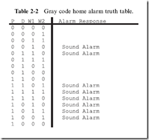
A much better method is to list the output responses in a truth table that is ordered using Gray codes, as I have shown in Table 2-2. Gray codes are a numbering system in which only one bit changes at a time: they are explained in detail along with how they are generated in Chapter 4. When you are listing data, regardless of the situation, you should always default to using Gray code inputs instead of incrementing binary inputs, as I have shown in Table 2-1.
Taking this advice, I recreated the home alarm system truth table using Gray codes in Table 2-2. When you look at Table 2-2, you should notice that the ‘‘discontinuities’’ of Table 2-1 have disappeared. The bit patterns which ‘‘Sound Alarm’’ group together quite nicely.
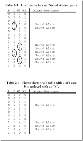
Looking at each value which ‘‘Sound Alarm’’, you’ll notice that each pair has three bits in common. To illustrate this, in Table 2-3, I have circled the bit which is different between each of the four pairs. In each of these
pairs, to sound the alarm we have very specific requirements for three bits, but the fourth bit can be in either state.
Another way of saying this is: for the alarm to sound, we don’t care what the fourth bit is and it can be ignored when we are determining the sum of products equation for the logic function. To indicate the ‘‘don’t care’’ bit, in Table 2-4, I have combined the bit pairs and changed the previously circled bits with an ‘‘x’’. This ‘‘x’’ indicates that the bit can be in either state for the output to be true. By replacing the two truth table entries with a single one with the don’t care bit indicated by an ‘‘x’’ you should see that something magical is starting to happen.
The obvious observation is that the table is shorter, but you should notice that the number of events which ‘‘Sound Alarm’’ has been halved and they are less complex than the eight original events. The sum of products equation for the bits shown in Table 2-4 is:
This sum of products expression will require four NOT gates, eight AND gates and three OR gates and the maximum gate delay will be nine. This has reduced the total gate count to less than 50% of the original total and this logic equation will operate somewhat faster than the original.
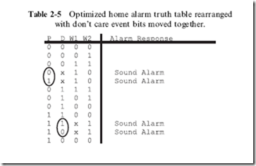
This is pretty good improvement in the logic circuit. You should be asking yourself if we can do better. To see if we can do better, I rearranged the data
in Table 2-4 so that the ‘‘Sound Alarm’’ events with common don’t care bits were put together and came up with Table 2-5. When I put the ‘‘Sound Alarm’’ events that had the same don’t care bits together, I noticed that in each of these cases, two of the remaining bits were in common and one bit changed in the two events (which I circled in Table 2.5). In Table 2-5, you may have noticed that the single changing bit of the original Gray code input sequence has been lost; this is not a problem. The Gray code sequence has served its purpose – it has indicated the initial input patterns which are common with its neighbors. In complex truth tables, you may have to rearrange bit patterns multiple times to find different
commonalities. When you do this, don’t worry about ‘‘loosing data’’; the important bit patterns are still saved in the active bit patterns.
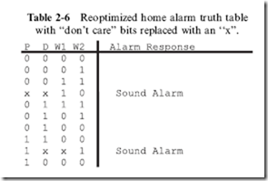
Table 2-6 shows what happens when the second don’t care bit is indicated. Since the two events which ‘‘Sound Alarm’’ do not have common don’t care bits, we can’t repeat this process any more. The two events from Table 2-6 can be written out as the sum of products:
This optimized ‘‘Alarm State’’ truth table has reduced our component count to one NOT gate, two AND gates and one OR gate and executes in five gate delays – quite an improvement from the original 43 gates and 11 gate delays!
Depending on how cynical you are, you might think that I ‘‘cooked up’’ this example to come up with such a dramatic improvement. Actually, the application shown here was my first attempt at coming up with a logic circuit to demonstrate how optimization operations of a logic circuit are performed; you will find similar improvements as this one when you start with a basic logic circuit and want to see how much you can reduce it.
Karnaugh Maps
Using truth tables is an effective but not very efficient method of optimizing digital logic circuits. A very clever French mathematician, Maurice Karnaugh (pronounced ‘‘carno’’) came up with a way to simplify the truth table optimization process by splitting the truth table inputs down the middle and arranging the two halves perpendicularly in order to display the relationships between bits more effectively. These modified truth tables are called ‘‘Karnaugh Maps’’ and are best suited for single bit output functions with three to six input bits.
My description of what a Karnaugh map is may sound cursory, but it is actually very accurate. A standard truth table can be considered to be a single dimensional presentation of a logic function and when it is properly manipulated, relationship between active outputs can be observed as I showed in the previous section. The problem with this method is that it is fairly labor intensive and will burn up a lot of paper. Karnaugh maps present the data in a two-dimensional ‘‘field’’ which allows for quick scanning of active output bits against their inputs, to find basic relationships between them.
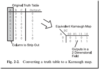
An example of converting a three input logic function from a truth table to a Karnaugh map is shown in Fig. 2-2. The initial logic function would be:
To create the Karnaugh map, I created a two by four matrix, with the rows being given the two different values for ‘‘A’’ and the columns given the four different values for ‘‘B’’ and ‘‘C’’. Note that the columns are listed as a two bit Gray code – this is an important feature of the Karnaugh map and, as I have pointed out, an important tool to being able to optimize a function. Once the two axes of the Karnaugh map are chosen, the outputs from the truth table are carefully transferred from the truth table to the Karnaugh map. When transferring the outputs, treat the Karnaugh map as a two-dimensional array, with the ‘‘X’’ dimension being the inputs which
weren’t stripped out and the ‘‘Y’’ dimension being the inputs which were stripped out from the truth table. When you are first starting out, this will be an operation in which you will tend to make mistakes because it is unfamiliar to you. To make sure you understand the process, it is a good idea to go back and convert your Karnaugh map into a truth table and compare it to your original truth table.
When you have created the Karnaugh map for your function, it is a good idea to either photocopy it or write it out in pen before going on. I am suggesting this action because, just as you did with the truth table, you are going to circle outputs which have the same unchanging bit patterns. As you circle the outputs, chances are you are not going to see the most effective groups of bits to circle together, or you will find that you have made a mistake in circling the bits. A photocopy or list in ink will allow you to try again without having to redraw the Karnaugh map.
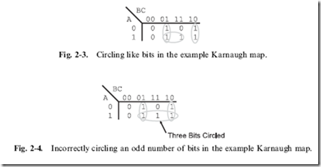
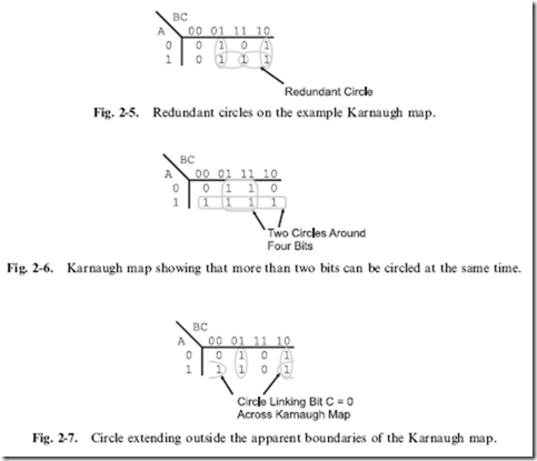
For the example shown in Fig. 2-2, the Karnaugh map has three circles put on it, as shown in Fig. 2-3. Each circle should result in combining two input sets together and making at least one bit into a ‘‘don’t care’’. Correctly circling bits can be difficult to understand, but there are a few rules that can be applied to it. First, each circle must be around a power of two number of bits – you cannot circle three bits (as shown in Fig. 2-4 for this example). Secondly, it is not a problem if circles overlap over specific bits. I should point out that there is the case for redundant circles (Fig. 2-5). If a circle is drawn and all the circled bits are enclosed in another circle, then the enclosed circle is redundant. Thirdly, remember that when you are circling bits that you want to circle a power of two number of bits, not just two. In Fig. 2-6, I have modified the three bit Karnaugh map with the outputs at A = 0 and B = C = 1 and A = 1 and B = C = 0 being a ‘‘1’’
and found that I could circle two groups of four bits. In each of these cases, I have made two bits ‘‘don’t care’’.
Finally, saying that a Karnaugh map is like a two-dimensional array is
inaccurate – it is actually a continuum unto itself, with the tops and sides being connected. When you draw out your Karnaugh map, you may find that the bits which can be circled (meaning ones with similar patterns) are on opposite ends of the Karnaugh map. This is not a problem as long as there are matching bits.
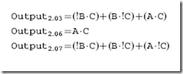
Once you have the outputs circled, you can now start writing out the optimized equation. As an exercise, you might want to look at the example Karnaugh maps in Figs. 2-3, 2-6 and 2-7. The output equations for these figures are:.
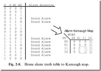
In this chapter, I wanted to show how the different optimizing tools are used for the home alarm system presented in the chapter introduction. The alarm system’s functions can be optimized using the Karnaugh map shown in Fig. 2-8. In Fig. 2-8, I have drawn the circles around the two groups of four active output bits which are in common and result in the logic equation
which is identical to the equation produced by the truth table reduction and a lot less work.
Before going on, I want to just say that once you are comfortable with Karnaugh maps, you will find them to be a fast and efficient method of optimizing simple logic functions. Becoming comfortable and being able to accurately convert the information from a truth table to a Karnaugh map will take some time, as will correctly circling active outputs to produce the optimized sum of products circuit. Once you have mastered this skill, you will find that you can go directly to the Karnaugh map from the requirements without the initial step of writing out the truth table.
