Equivalent-Time Sampling
If real-time sampling techniques are not fast enough to digitize the signal, then consider ETS as an approach. Unlike continuous, interval, or multirate scanning, complex counter/timers control ETS conversions, and ETS strictly requires that the input waveform be repetitive throughout the entire sampling period.
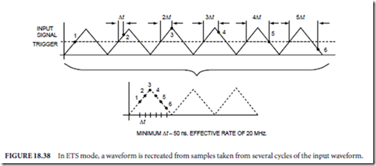
In ETS mode, an analog trigger arms a counter, which triggers an ADC conversion at progressively increasing time intervals beyond the occurrence of the analog trigger (as shown in Fig. 18.38). Instead of acquiring samples in rapid succession, the ADC digitizes only one sample per cycle. Samples from several cycles of the input waveform are then used to recreate the shape of the signal.
ETS Counter/Timer Operations
Four complex timing and triggering mechanisms are necessary for ETS. They include hardware analog triggering, retriggerable pulse generation, autoincrementing, and flexible data acquisition signal routing.
Hardware Analog Triggering
Analog trigger circuitry monitors the input voltage of the waveform and generates a pulse whenever the trigger conditions are met. Each time the repetitive waveform crosses the trigger level, the analog trigger circuitry arms the board for another acquisition.
Retriggerable Pulse Generation
The ADC samples when it receives a pulse for the conversion counter. In real-time sampling, the conversion counter generates a series of continuous pulses that cause the ADC to successively digitize multiple values. In ETS, however, the conversion counter generates only one pulse, which corresponds to one sample from one cycle of the waveform. This pulse is regenerated in response to a signal from the analog trigger circuitry, which occurs after each new cycle of the waveform.
Autoincrementing
If the ADC sampled every occurrence of the waveform using only retriggerable pulse generation, the same point along the repetitive signal would be digitized, namely, the point corresponding to the analog trigger. A method is needed to make the ADC sample different points along different cycles of the waveform. This method, known as autoincrementing, is the most important counter/timer functional for controlling ETS. An autoincrementing counter produces a series of delayed pulses.
Flexible Data Acquisition Signal Routing
As with seamlessly changing the sample rate, ETS uses signals from other parts of the board to control ADC conversions. The DAQ-STC generates autoincrementing retriggerable pulses.
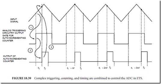
Figure 18.39 details the timing signals used for ETS. As the input waveform crosses the trigger voltage 1, the analog trigger circuitry generates a pulse at the gate input of the autoincrementing counter. This counter generates a conversion pulse 2, which is used to trigger the ADC to take a sample 3. The timing process continues until a predetermined number of samples has been acquired. The delay time Dt is directly related to the relative sampling rate set. For example, for an effective sampling rate of 20 MS/s, Dt is equal to 50 ns. Because the waveform is repetitive over the complete acquisition, the points in the recreated waveform appear as if they were taken every 50 ns.
Considerations When Using ETS
Although ETS is useful in a number of applications, ETS users need to be aware of a few issues. First, the input waveform must be repetitive. ETS will not correctly reproduce a waveform that is nonrepetitive because the analog trigger will never occur at the same place along the waveform. One-shot acquisitions are not possible, because ETS digitizes a sample from several cycles of a repetitive waveform.
The accuracy of the conversion is limited to the accuracy of the counter/timer. Jitter in the counter/timer causes the sample to be taken within a multiple of 50 ns from the trigger. The sample may occur along a
slightly different portion of the input waveform than expected. For example, using a 12-b board to sample the 100-Hz, 10-V peak-to-peak sine wave in Fig. 18.31, the accuracy error is 0.13 LSB.
ETS techniques are useful in measuring the rise and fall times of TTL signals. ETS is also used to measure the impulse response of a 1-MHz, low-pass filter subject to a 2-ms repetitive impulse. The impulse response is a repetitive signal of pulses that also have a duration of 2 ms. Using a 20-MHz ETS conversion rate results in 40 digitized samples per input impulse. This is enough samples to display the impulse response in the time domain. Other applications for ETS include disk drive testing, nondestructive testing, ultrasonic testing, vibration analysis, laser diode characterization, and impact testing.
Factors Influencing the Accuracy of Your Measurements
How do you tell if the plug-in data acquisition board that you already have or the board that you are considering integrating into your system will give you the results you want? With a sophisticated measuring device like a plug-in DAQ board, you can obtain significantly different accuracies depending on which board you are using. For example, you can purchase DAQ products on the market today with 16-b analog to digital converters and get less than 12 b of useful data, or you can purchase a product with a 16-b ADC and actually get 16 b of useful data. This difference in accuracies causes confusion in the PC industry where everyone is used to switching out PCs, video cards, printers, and so on, and experiencing similar results between equipment.
The most important thing to do is to scrutinize more specifications than the resolution of the A/D converter that is used on the DAQ board. For DC-class measurements, you should at least consider the settling time of the instrumentation amplifier, differential non-linearity (DNL), relative accuracy, integral nonlinearity (INL), and noise. If the manufacturer of the board you are considering does not supply you with each of these specifications in the data sheets, you can ask the vendor to provide them or you can run tests yourself to determine these specifications of your DAQ board.
Linearity
Ideally, as you increase the level of voltage applied to a DAQ board, the digital codes from the ADC should also increase linearly. If you were to plot the voltage vs. the output code from an ideal ADC, the plot would be a straight line. Deviations from this ideal straight line are specified as the nonlinearity. Three specifications indicate how linear a DAQ boards transfer function is: differential nonlinearity, relative accuracy, and integral nonlinearity.
Differential Nonlinearity
For each digital output code, there is a continuous range of analog input values that produce it. This range is bounded on either side by transitions. The size of this range is known as the code width. Ideally, the width of all binary code values is identical and is equal to the smallest detectable voltage change,
where n is the resolution of the ADC. For example, a board that has a 12-b ADC, input range of 0–10, and a gain of 100 will have an ideal code width of
This ideal analog code width defines the analog unit called the least significant bit. DNL is a measure in LSB of the worst-case deviation of code widths from their ideal value of 1 LSB. An ideal DAQ board has a DNL of 0 LSB. Practically, a good DAQ board will have a DNL within ±0.5 LSB.
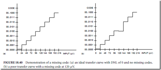
There is no upper limit on how wide a code can be. Codes do not have widths of less than 0 LSB, so the DNL is never worse than −1 LSB. A poorly performing DAQ board may have a code width equal to or very near zero, which indicates a missing code. No matter what voltage you input to the DAQ board with a missing code, the board will never quantize the voltage to the value represented by this code. Sometimes DNL is specified by stating that a DAQ board has no missing codes, which means that the DNL is bounded below by −1 LSB but does not make any specifications about the upper bound.
If the DAQ board in the previous example had a missing code at 120 µV, then increasing the voltage from 96 to 120 µV would not be detectable. Only when the voltage is increased another LSB, or in this example, 24 µV, will the voltage change be detectable (Fig. 18.40). As you can see, poor DNL reduces the resolution of the board.
To run your own DNL test:
1. Input a high-resolution, highly linear triangle wave into one channel of the DAQ board. The frequency of the triangle should be low and the amplitude should swing from minus full scale to plus full scale of the input to the DAQ board.
2. Start an acquisition on the plug-in board so that you acquire a large number of points. Recom- mended values are 1 × 10⁶ samples for a 12-b board and 20 × 106 million samples for a 16-b board.
3. Make a histogram of all the acquired binary codes. This will give you the relative frequency of each code occurrence.
4. Normalize the histogram by dividing by the averaged value of the histogram.
5. The DNL is the greatest deviation from the value of 1 LSB. Because the input was a triangle wave, it had a uniform distribution over the DAQ board codes. The probability of a code occurring is directly proportional to the code width, and therefore shows the DNL.
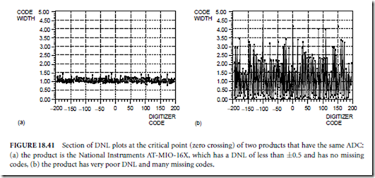
Figure 18.41 shows a section of the DNL plot of two products with the same 16-b ADC yet significantly different DNL. Ideally, the codewidth plot will be a straight line at 1 LSB. Figure 18.41(a) shows the codewidth plot of a product that has DNL of less than ±0.5 LSB. Because the codewidth is never 0, the product also has no missing codes. Figure 18.41(b) shows the codewidth plot of a product that has poor DNL. This product has many missing codes, a code width that is as much as 4.2 LSB at the code value 0, and is clearly not 16-b linear.
Relative Accuracy
Relative accuracy is a measure in LSBs of the worst-case deviation from the ideal DAQ board transfer function, a straight line. To run your own relative accuracy test:
1. Connect a high-accuracy analog voltage-generation source to one channel of the DAQ board. The source should be very linear and have a higher resolution than the DAQ board that you wish to test.
2. Generate a voltage that is near minus full scale.
3. Acquire at least 100 samples from the DAQ board and average them. The reason for averaging is to reduce the effects of any noise that is present.
4. Increase the voltage slightly and repeat step 3. Continue steps 3 and 4 until you have swept through the input range of the DAQ board.
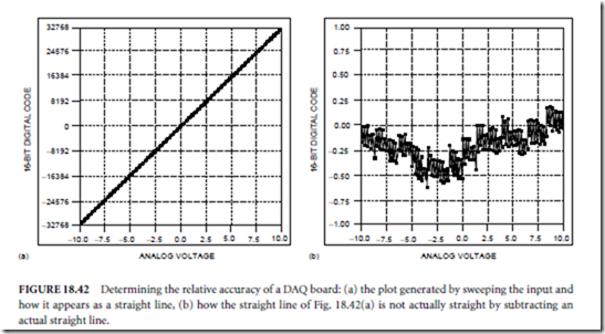
5. Plot the averaged points on the computer. You will have a straight line, as shown in Fig. 18.42(a), unless the relative accuracy of your DAQ board is astonishingly bad.
6. To see the deviation from a straight line, you must first generate an actual straight line in software that starts at the minus full-scale reading and ends at the plus full-scale reading using a straight-line endpoint fit analysis routine.
7. Subtract the actual straight line from the waveform that you acquired. If you plot the resulting array, you should see a plot similar to Fig. 18.42(b).
8. The maximum deviation from zero is the relative accuracy of the DAQ board.
The driver software for a DAQ board will translate the binary code value of the ADC to voltage by multiplying by a constant. Good relative accuracy is important for a DAQ board because it ensures that the translation from the binary code of the ADC to the voltage value is accurate. Obtaining good relative accuracy requires that both the ADC and the surrounding analog support circuitry be designed properly.
Integral Nonlinearity
INL is a measure in LSB of the straightness of a DAQ board’s transfer function. Specifically, it indicates how far a plot of the DAQ boards transitions deviates from a straight line. Factors that contribute to poor INL on a DAQ board are the ADC, multiplexer, and instrumentation amplifier. The INL test is the most difficult to make:
1. Input a signal from a digital to analog converter that has higher resolution and linearity than the DAQ board that you are testing.
2. Starting at minus full scale, increase the codes to the DAC until the binary reading from the ADC flickers between two consecutive values. When the binary reading flickers evenly between codes, you have found the LSB transition for the DAQ board.
3. Record the DAC codes of all transitions.
4. Using an analysis routine, make an endpoint fit on the recorded DAC codes.
5. Subtract the endpoint fit line from the recorded DAC values.
6. The farthest deviation from zero is the INL.
Even though highly specified, the INL specification does not have as much value as the relative accuracy specification and is much more difficult to make. The relative accuracy specification is showing the deviation from the ideal straight line whereas the INL is showing the deviation of the transitions from an ideal straight line. Therefore, relative accuracy takes the quantization error, INL, and DNL into consideration.
Settling Time
On a typical plug-in DAQ board, an analog signal is first selected by a multiplexer, and then amplified by an instrumentation amplifier before it is converted to a digital signal by the ADC. This instrumentation amplifier must be able to track the output of the multiplexer as the multiplexer switches channels, and the instrumentation amplifier must be able to settle to the accuracy of the ADC. Otherwise, the ADC will convert an analog signal that has not settled to the value that you are trying to measure with your DAQ board. The time required for the instrumentation amplifier to settle to a specified accuracy is called the settling time. Poor settling time is a major problem because the amount of inaccuracy usually varies with gain and sampling rate. Because the errors occur in the analog stages of the DAQ board, the board cannot return an error message to the computer when the instrumentation amplifier does not settle.
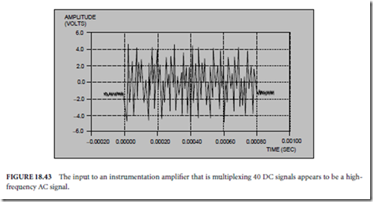
The instrumentation amplifier is most likely not to settle when you are sampling multiple channels at high gains and high rates. When the application is sampling multiple channels, the multiplexer is switching among different channels that can have significant differences in voltage levels (Fig. 18.43). Instrumentation amplifiers can have difficulty tracking this significant difference in voltage. Typically, the higher the gain and the faster the channel switching time, the less likely it is that the instrumentation amplifier will settle. It is important to be aware of settling time problems so you know at what multichannel rates and gains you can run your DAQ board and maintain accurate readings. Running your own settling time test is relatively easy:
1. Apply a signal to one channel of your DAQ board that is nearly full scale. Be sure to take the range and gain into account when you select the levels of the signal you will apply. For example, if you are using a gain of 100 on a ±10 V input range on the DAQ board, apply a signal slightly less than 10 V/100 or +0.1-V signal to the channel.
2. Acquire at least 1000 samples from one channel only and average them. The averaged value will be the expected value of the DAQ board when the instrumentation amplifier settles properly.
3. Apply a minus full-scale signal to a second channel. Be sure to take range and gain into account, as described earlier.
4. Acquire at least 1000 samples from the second channel only and average them. This will give you the expected value for the second channel when the instrumentation amplifier settles properly.
5. Have the DAQ board sample both channels at the highest possible sampling rate so that the multiplexer is switching between the first and the second channels.
6. Average at least 100 samples from each channel.
7. The deviation between the values returned from the board when you sampled the channels using a single channel acquisition and the values returned when you sampled the channels using a multichannel acquisition will be the settling time error.
To plot the settling time error, repeat steps 5 and 6, but reduce the sampling rate each time. Then plot the greatest deviation at each sampling rate. A DAQ board settles to the accuracy of the ADC only when the settling time error is less than ±0.5 LSB. By plotting the settling time error, you can determine at what rate you can sample with your DAQ board and settle to the accuracy that your application requires. The settling-time plot will usually vary with gain and so you will want to repeat the test at different gains.
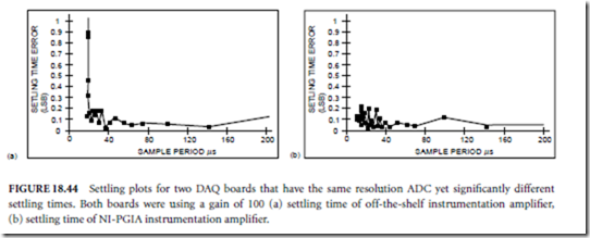
Figure 18.44 shows an example of two DAQ boards that have a 12-b resolution ADC, yet have significantly different settling times. For the tests, both boards were sampling two channels with a gain of 100. The settling-time plot for the first board, shown in Fig. 18.44(a), uses an off-the-shelf instrumentation amplifier, which has 34 LSBs of settling-time error when sampling at 100 kHz. Because the board was using an input range of 20 V at a gain of 100, 1 LSB = 48.8 µV. Therefore, data are inaccurate by as much as 1.7 mV due
to settling-time when the board is sampling at 100 kHz at a gain of 100. If you use this board you must either increase the sampling period to greater than 20 µs so that the board can settle, or be able to accept the settling-time inaccuracy. The settling-time plot for the second board, shown in Fig. 18.44(b), settles properly because it uses a custom instrumentation amplifier designed specifically to settle in DAQ board applications. Because the board settles to within ±0.5 LSB at the maximum sampling rate, you can run the board at all sampling rates and not have any detectable settling-time error.
Applications that are sampling only one channel, applications that are sampling multiple channels at very slow rates, or applications that are sampling multiple channels at low gains usually do not have a problem with settling time. For the other applications, your best solution is to purchase a DAQ board that will settle at all rates and all gains. Otherwise, you will have to either reduce your sampling rate or realize that your readings are not accurate to the specified value of the ADC.
Noise
Noise is any unwanted signal that appears in the digitized signal of the DAQ board. Because the PC is a noisy digital environment, acquiring data on a plug-in board takes a very careful layout on multilayer DAQ boards by skilled analog designers. Designers can use metal shielding on a DAQ board to help reduce noise. Proper shielding should not only be added around sensitive analog sections on a DAQ board, but must also be built into the DAQ board with ground planes.
Of all of the tests to run, a DC-class signal noise test is the easiest to run:
1. Connect the + and − inputs of the DAQ board directly to ground. If possible, make the connection directly on the I/O connector of the board. By doing this, you can measure only the noise introduced by the DAQ board instead of noise introduced by your cabling.
2. Acquire a large number of points (1 × 10⁶) with the DAQ board at the gain you choose in your application.
3. Make a histogram of the data and normalize the array of samples by dividing by the total number of points acquired.
4. Plot the normalized array.
5. The deviation, in LSB, from the highest probability of occurrence is the noise.
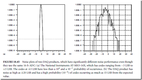
Figure 18.45 shows the DC-noise plot of two DAQ products, both of which use the same ADC. You can determine two qualities of the DAQ board from the noise plots—range of noise and the distribution.
The plot in Fig. 18.45(a) has a high distribution of samples at 0 and a very small number of points occurring at other codes. The distribution is Gaussian, which is what is expected from random noise. From the plot, the noise level is within ±3 LSB. The plot in Fig. 18.45(b) is a very noisy DAQ product, which does not have the expected distribution and has a noise greater than ±20 LSB, with many samples occurring at points other than the expected value. For the DAQ product in Fig. 18.45(b), the tests were run with an input range of ±10 V and a gain of 10. Therefore, 1 LSB = 31 µV, thus a noise level of 20 LSB is equivalent to 620 µV of noise.
