Data Acquisition Software
The software is often the most critical component of the data acquisition system. Properly chosen software can save you a great deal of time and money. Likewise, poorly chosen software can cost you time and money. A whole spectrum of software options exists, with important tradeoffs and advantages.
Board Register-Level Programming
The first option is not to use vendor-supplied software and program the DAQ board yourself at the hardware level. DAQ boards are typically register based, that is, they include a number of digital registers that control the operation of the board. The developer may use any standard programming language to write series of binary codes to the DAQ board to control its operation.
Driver Software
![]() Driver software typically consists of a library of function calls usable from a standard programming language. These function calls provide a high-level interface to control the standard functions of the plug- in board. For example, a function called SCAN OP may configure, initiate, and complete a multiple channel scanning data acquisition operation of a predetermined number of points. The function call would include parameters to indicate the channels to be scanned, the amplifier gains to be used, the sampling rate, and the total number of data points to collect. The driver responds to this one function call by programming the plug-in board, the DMA controller, the interrupt controller, and CPU to scan the channels as requested.
Driver software typically consists of a library of function calls usable from a standard programming language. These function calls provide a high-level interface to control the standard functions of the plug- in board. For example, a function called SCAN OP may configure, initiate, and complete a multiple channel scanning data acquisition operation of a predetermined number of points. The function call would include parameters to indicate the channels to be scanned, the amplifier gains to be used, the sampling rate, and the total number of data points to collect. The driver responds to this one function call by programming the plug-in board, the DMA controller, the interrupt controller, and CPU to scan the channels as requested.
Digital Sampling
Every DAQ system has the task of gathering information about analog signals. To do this, the system captures a series of instantaneous snapshots or samples of the signal at definite time intervals. Each sample contains information about the signal at a specific instant. Knowing the exact conversion time and the value of the sample, you can reconstruct, analyze, and display the digitized waveform.
Two classifications of sample timing techniques are used to control the ADC conversions, real-time sampling and equivalent-time sampling (ETS). Depending on the type of signal you acquire and the rate of acquisition, one sampling technique may be better than the other.
Real-Time Sampling Techniques
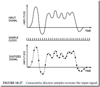
In real-time sampling, you immediately see the changes, as the signal changes (Fig. 18.27). According to the Nyquist theorem, you must sample at least twice the rate of the maximum frequency component in that signal to prevent aliasing. The frequency at one-half the sampling frequency is referred to as the Nyquist frequency. Theoretically, it is possible to recover information about those signals with frequencies at or below the Nyquist frequency. Frequencies above the Nyquist frequency will alias to appear between DC and the Nyquist frequency.
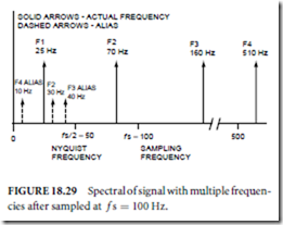
For example, assume the sampling frequency f s, is 100 Hz. Also assume the input signal to be sampled contains the following frequencies: 25, 70, 160, and 510 Hz. Figure 18.28 shows a spectral representation of the input signal. The mathematics of sampling theory show us that a sampled signal is shifted in the frequency domain by an amount equal to integer multiples of the sampling frequency, f s.
Figure 18.29 shows the spectral content of the input signal after sampling. Frequencies below 50 Hz, the NYQUIST FREQUENCY SAMPLING FREQUENCY Nyquist frequency ( f s/2), appear correctly. How ever, frequencies above the Nyquist appear as aliases below the Nyquist frequency. For example, F1 appears correctly; however, both F2, F3, and F4 have aliases at 30, 40, and 10 Hz, respectively.
The resulting frequency of aliased signals can be calculated with the following formula:
Preventing Aliasing
You can prevent aliasing by using filters on the front end of your DAQ system. These antialiasing filters are set to cut off any frequencies above the Nyquist frequency (half the sampling rate). The perfect filter would reject all frequencies above the Nyquist; how ever, because perfect filters exist only in textbooks, you must compromise between sampling rate and selecting filters. In many applications, one- or two pole passive filters are satisfactory. By oversampling (5–10 times) and using these filters, you can sample adequately in most cases.
Alternatively, you can use active antialiasing filters with programmable cutoff frequencies and very sharp attenuation of frequencies above the cutoff.
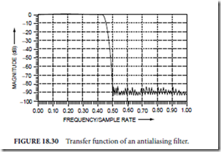
Because these filters exhibit a very steep rolloff, you can sample at two to three times the filter cutoff frequency. Figure 18.30 shows a transfer function of a high-quality antialiasing filter.
The computer uses digital values to recreate or to analyze the waveform. Because the signal could be anything between each sample, the DAQ board may be unaware of any changes in the signal between samples. There are several sampling methods optimized for the different classes of data; they include software polling, external sampling, continuous scanning, multirate scanning, simultaneous sampling, interval scanning, and seamless changing of the sample rate.
Software Polling
A software loop polls a timing signal and starts the ADC conversion via a software command when the edge of the timing signal is detected. The timing signal may originate from the computer’s internal clock or from a clock on the DAQ board. Software polling is useful in simple, low-speed applications, such as temperature measurements.
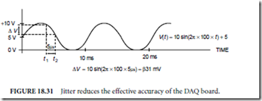
The software loop must be fast enough to detect the timing signal and trigger a conversion. Otherwise, a window of uncertainty, also known as jitter, will exist between two successive samples. Within the window of uncertainty, the input waveform could change enough to drastically reduce the accuracy of the ADC.
Suppose a 100-Hz, 10-V full-scale sine wave is digitized (Fig. 18.31). If the polling loop takes 5 ms to detect the timing signal and to trigger a conversion, then the voltage of the input sine wave will change as much as 31 mV (ΛV − 10 sin(2π × 100 × 5 × 10−6)). For a 12-b ADC operating over an input range of 10 V and a gain of 1, 1 least significant bit (LSB) of error represents 2.44 mV
External Sampling
Some DAQ applications must perform a conversion based on another physical event that triggers the data conversion. The event could be a pulse from an optical encoder measuring the rotation of a cylinder. A sample would be taken every time the encoder generates a pulse corresponding to n degrees of rotation. External triggering is advantageous when trying to measure signals whose occurrence is relative to another physical phenomena.
Continuous Scanning
When a DAQ board acquires data, several components on the board convert the analog signal to a digital value. These components include the analog multiplexer (mux), the instrumentation amplifier, the sample- and-hold circuitry, and the ADC. When acquiring data from several input channels, the analog mux connects each signal to the ADC at a constant rate. This method, known as continuous scanning, is significantly less expensive than having a separate amplifier and ADC for each input channel.
Continuous scanning is advantageous because it eliminates jitter and is easy to implement. However, it is not possible to simultaneously sample multiple channels. Because the mux switches between channels, a time skew occurs between any two successive channel samples. Continuous scanning is appropriate for applications where the time relationship between each sampled point is unimportant or where the skew is relatively negligible compared to the speed of the channel scan.
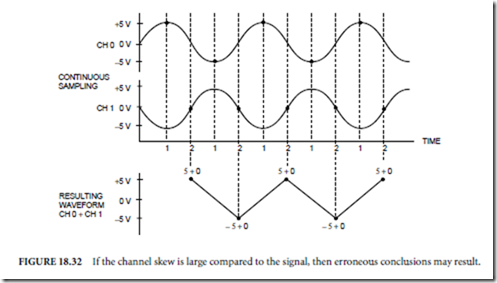
If you are using samples from two signals to generate a third value, then continuous scanning can lead to significant errors if the time skew is large. In Fig. 18.32, two channels are continuously sampled and added together to produce a third value. Because the two sine waves are 90◦ out of phase, the sum of the signals should always be zero. But because the skew time between the samples, an erroneous sawtooth signal results.
Multirate Scanning
Multirate scanning, a method that scans multiple channels at different scan rates, is a special case of continuous scanning. Applications that digitize multiple signals with a variety of frequencies use multirate scanning to minimize the amount of buffer space needed to store the sampled signals. You can use channel-independent ADCs to implement hardware multirate scanning; however, this method is extremely expensive. Instead of multiple ADCs, only one ADC is used. A channel/gain configuration register stores the scan rate per channel and software divides down the scan clock based on the per-channel scan rate. Software-controlled multirate scanning works by sampling each input channel at a rate that is a fraction of the specified scan rate.
Suppose you want to scan channels 0–3 at 10 kilosamples/sec, channel 4 at 5 kilosamples/sec, and channels 5–7 at 1 kilosamples/sec. You should choose a base scan rate of 10 kilosamples/sec. Channels 0–3 are acquired at the base scan rate. Software and hardware divide the base scan rate by 2 to sample channel 4 at 5 kilosamples/sec, and by 10 to sample channels 5–7 at 1 kilosamples/sec.
Simultaneous Sampling
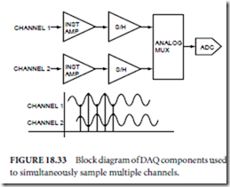
For applications where the time relationship between the input signals is important, such as phase analysis of AC signals, you must use simultaneous sampling. DAQ boards capable of simultaneous sampling typically use independent instrumentation amplifiers and sample-and-hold circuitry for each input channel, along with an analog mux, which routes the input signals to the ADC for conversion (as shown in Fig. 18.33).
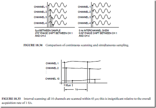
To demonstrate the need for a simultaneous- sampling DAQ board, consider a system consist- ing of four 50-kHz input signals sampled at 200 kilosamples/sec. If the DAQ board uses continuous scanning, the skew between each channel is 5 µs (1 S/200 kilosamples/sec) which represents a 270◦ (15 µs/20 µs × 360◦) shift in phase between the first channel and fourth channel. Alternately, with a simultaneous-sampling board with a maximum 5 ns interchannel time offset, the phase shift is only 0.09◦ (5 ns/20 µs × 360◦). This phenomenon is illustrated in Fig. 18.34.
Interval Scanning
For low-frequency signals, interval scanning creates the effect of simultaneous sampling, yet maintains the cost benefits of a continuous scanning system. This method scans the input channels at one rate and uses a second rate to control when the next scan begins. You can scan the input channels at the fastest rate of the ADC, creating the effect of simultaneous sampling. Interval scanning is appropriate for slow moving signals, such as temperature and pressure. Interval scanning results in a jitter-free sample rate and minimal skew time between channel samples. For example, consider a DAQ system with 10 temperature signals. Using interval scanning, you can set up the DAQ board to scan all channels with an interchannel delay of 5 µs, then repeat the scan every second. This method creates the effect of simultaneously sampling 10 channels at 1 S/s, as shown in Fig. 18.35.
To illustrate the difference between continuous and interval scanning, consider an application that monitors the torque and revolutions per minute (RPMs) of an automobile engine and computes the engine horsepower. Two signals, proportional to torque and RPM, are easily sampled by a DAQ board at a rate of 1000 S/s. The values are multiplied together to determine the horsepower as a function of time. A continuously scanning DAQ board must sample at an aggregate rate of 2000 S/s. The time between which the torque signal is sampled and the RPM signal is sampled will always be 0.5 ms (1/2000). If either signal changes within 0.5 ms, then the calculated horsepower is incorrect. But using interval scanning at a rate of 1000 S/s, the DAQ board samples the torque signal every 1 ms, and the RPM signal is sampled as quickly as possible after the torque is sampled. If a 5-µs interchannel delay exists between the torque and RPM samples, then the time skew is reduced by 99% ((0.5 ms − 5 µs))/0.5 ms), and the chance of an incorrect calculation is reduced.
Seamless Changing of the Sampling Rate
This technique, a variation of real-time sampling, is used to vary the sampling rate of the ADC without having to stop and reprogram the counter/timer for different conversion rates. For example, you may want to start sampling slowly, and then, following a trigger, begin sampling quickly; this is particularly useful when performing transient analysis. The ADC samples slowly until the input crosses a voltage level, and then the ADC samples quickly to capture the transient.
Four complex timing and triggering mechanisms are necessary to seamlessly change the sampling rate. They include hardware analog triggering, frequency shift keying (FSK), flexible data acquisition signal routing, and buffered relative-time stamping.
Hardware Analog Triggering
A trigger level serves as the reference point at which the sampling rate changes. Analog trigger circuitry monitors the input voltage of the waveform and generates a transistor-transmitter logic (TTL) high level whenever the voltage input is greater than the trigger voltage V set; and a TTL low level when the voltage input is less than the trigger voltage. Therefore, as the waveform crosses the trigger level, the analog trigger circuitry signals the counter to count at a different frequency.
Frequency Shift Keying
Frequency shift keying (FSK) occurs when the frequency of a digital pulse varies over time. Frequency modulation (FM) in the analog domain is analogous to FSK in the digital domain. FSK determines the frequency of a generated pulse train relative to the level present at the gate of a counter. For example, when the gate signal is a TTL high level, the pulse train frequency is three times greater than the pulse train frequency when the gate signal is a TTL low level.
Flexible Data Acquisition Signal Routing
For continuous or interval scanning, a simple, dedicated sample timer directly controls ADC conversions. But for more complex sampling techniques, such as seamlessly changing the sampling rate, signals from other parts of the DAQ board control ADC conversions. The DAQ-STC ASIC provides 20 possible signal sources to time each ADC conversion. One of the sources is the output of the general-purpose counter 0, which is more flexible than a dedicated timer. In particular, the general-purpose counter generates the FSK signal that is routed to the ADC to control the sampling rate.
Buffered Relative-Time Stamping
Because different sample rates are used to acquire the signal, keeping track of the various acquisition rates is a challenge for the board and software. The sampled values must have an acquisition time associated with them in order for the signal to be correctly displayed. While values are sampled by the ADC, the DAQ-STC counter/timers measure the relative time between each sample using a technique called buffered relative- time stamping. The measured time is then transferred from the counter/timer registers to PC memory via direct memory access.
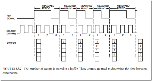
The counter continuously measures the time interval between successive, same-polarity transitions of the FSK pulse with a measurement resolution of 50 ns. Countings begin at 0. The counter contents are
stored in a buffer after an edge of the appropriate polarity is detected. Then, the counting begins again at 0. Software routines use DMA to transfer data from the counter to a buffer until the buffer is filled.
For example, in Fig. 18.36, the period of an FSK signal is measured. The first period is 150 ns (3 clock cycles × 50-ns resolution); the second, third, and fourth periods are 100 ns (2 clock cycles × 50 ns); the
fifth period is 150 ns. For a 10-MHz board that can change its sampling rate seamlessly, the FSK signal determines the ADC conversions; the effective sampling rate is 6.7 MHz for the first part of the signal and 10 MHz for the second part of the signal.
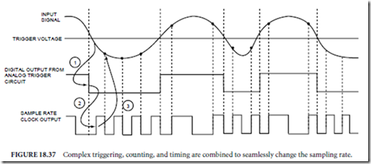
Figure 18.37 details the timing signals necessary to change the sampling rate of the ADC without missing data. As the input waveform crosses the trigger voltage 1 the analog trigger circuitry generates a low on its output. The output signal is routed to a general-purpose counter, which generates pulses at a predetermined frequency 2. Each high-to-low transition of the FSK signal causes the ADC to sample the waveform 3. When the input waveform crosses the trigger level again, the analog trigger circuit generates a high, which causes the general-purpose counter to generate pulses at a second frequency. This timing process continues until a predetermined number of samples has been acquired.
Considerations When Seamlessly Changing the Sampling Rate
The intention of seamlessly changing the sampling rate is to switch between rates, yet not miss significant changes in the signal. Selecting the various rates and the instance at which the rate changes requires some
thought. For instance, when switching between a sampling rate of 10 S/s and 20 kilosamples/sec, the analog trigger circuitry checks for a trigger condition every 1/10 of a second. This means that, at most, 0.1 s will pass before the DAQ board is aware of the trigger and increases the sampling rate to 20 kilosamples/sec. If the ADC is switching between a rate of 20 kilosamples/sec and 10 S/s, the trigger condition is checked every 50 ms, and the board will take, at most, 50 ms to switch to the 10 S/s rate. Thus, you should set the trigger condition so that you can detect the trigger and start the faster rate before the signal changes significantly.
Suppose automatic braking systems (ABS) are tested by monitoring signal transients. The test requires a few samples to be recorded before and after the transient, as well as the transient signal. The test specifies a sample rate of 400 kilosamples/sec. If the DAQ board continuously samples the system, you must sample the entire signal at 400 kilosamples/sec. For a signal that is stable for 1 min before the transient, then 24 × 106 samples are acquired before the transient even occurs. If the data are stored on disk, a large hard disk is needed. But if the stable portion of the signal is sampled more slowly, such as 40 S/s, the amount of unnecessary data acquired is reduced. If the sampling rate is changed on the fly, then the board can sample at 40 S/s before and after the transient and at 400 kilosamples/sec during the transient. In the 1 min before the transient, only 2400 samples are logged. Once the transient occurs, the board samples at 400 kilosamples/sec. Once the transient passes, the ADC begins to sample at 40 S/s again. Using this method, exactly the number of samples needed relative to the signal are logged to disk.
