7.3.4 ALU Design
Functionally, an ALU can be divided up into two segments: the arithmetic unit and the logic unit. The arithmetic unit performs typical arithmetic operations such as addition, subtraction, and increment or decrement by 1. Usually, the operands involved may be signed or unsigned integers. In some cases, however, an arithmetic unit must handle 4-bit binary-coded decimal (BCD) numbers and floating-point numbers. Therefore, this unit must include the circuitry necessary to manipulate these data types. As the name implies, the logic unit contains hardware elements that perform typical operations such as Boolean NOT and OR. In this section, the design of a simple ALU using typical combinational elements such as gates, multiplexers, and a 4-bit parallel adder is discussed. For this approach, an arithmetic unit and a logic unit are first designed separately; then they are combined to obtain an ALU.
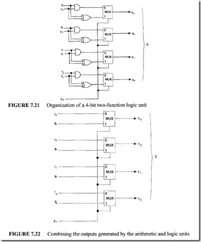
For the first step, a two-function arithmetic unit, as shown in Figure 7.20 is designed. The key element of this system is a 4-bit parallel adder. The multiplexers select
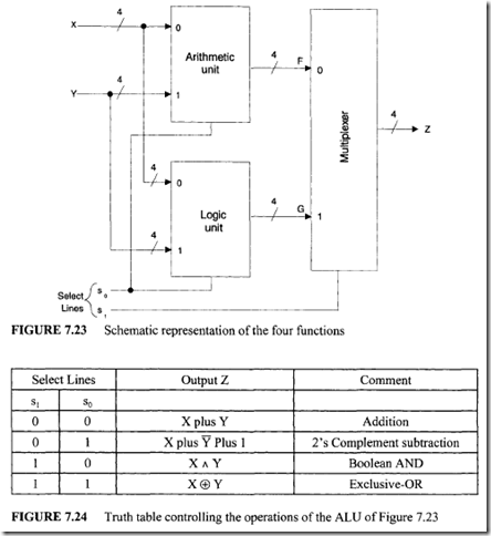
This arithmetic unit generates addition and subtraction operations. For the second step, let us design a two-function logic unit; this is shown in Figure 7.21. From Figure 7.21 it can be seen that when s0 = 0, the output G =X AND Y; otherwise the output G =X ![]() Y. Note that from these two Boolean operations, other operations such as NOT and OR can be derived by the following Boolean identities:
Y. Note that from these two Boolean operations, other operations such as NOT and OR can be derived by the following Boolean identities:
Therefore, NOT and OR operations can be obtained by using additional hardware and the circuit of Figure 7.21. The outputs generated by the arithmetic and logic units can be combined by using a set of multiplexers, as shown in Figure 7.22. From this organization it can be seen that when the select line s1 = 1, the multiplexers select outputs generated by the logic unit; otherwise, the outputs of the arithmetic unit are selected.
More commonly, the select line, s1, is referred to as the mode input because it selects the desired mode of operation (arithmetic or logic). A complete block diagram schematic of this ALU is shown in Figure 7.23. The truth table illustrating the operation of this ALU is shown in Figure 7.24. This table shows that this ALU is capable of performing 2 arithmetic and 2 logic operations on the 4-bit operands X and Y.
The rapid growth in IC technology permitted the manufacturers to produce an ALU as an MSI block. Such systems implement many operations, and their use as a system
component reduces the hardware cost, board space, debugging effort, and failure rate. Usually, each MSI ALU chip is designed as a 4-bit slice. However, a designer can easily interconnect n such chips to get a 4n-bit ALU. Some popular 4-bit ALU chips are the 74381 and 74181. The 74381 ALU performs 3 arithmetic and 2 miscellaneous operations on 4-bit operands. The 74181 ALU performs 16 arithmetic and 16 Boolean operations on two 4-bit operands, using either active high or active low data. A complete description and operational characteristics of these devices may be found in the data books.
Typical 8-bit microprocessors, such as the Intel 8085 and Motorola 6809, do not include multiplication and division instructions due to limitations in the circuit densities that can be placed on the chip. Due to advanced semiconductor technology, 16-, 32-, and 64-bit
microprocessors usually include multiplication and division algorithms in a ROM inside the chip. These algorithms typically utilize an ALU to carry out the operations. Verilog and VHDL descriptions along with simulation results of typical ALU’s are included in Appendices I and J respectively.
7.3.5 Design of the Control Unit
The main purpose of the control unit is to translate or decode instructions and generate appropriate enable signals to accomplish the desired operation. Based on the contents of the instruction register, the control unit sends the selected data items to the appropriate processing hardware at the right time. The control unit drives the associated processing hardware by generating a set of signals that are synchronized with a master clock.
The control unit performs two basic operations: instruction interpretation and instruction sequencing. In the interpretation phase, the control unit reads (fetches) an instruction from the memory addressed by the contents of the program counter into the instruction register. The control unit inputs the contents of the instruction register. It recognizes the instruction type, obtains the necessary operands, and routes them to the appropriate functional units of the execution unit (registers and ALU). The control unit then issues the necessary signals to the execution unit to perform the desired operation and routes the results to the specified destination.
In the sequencing phase, the control unit generates the address of the next instruction to be executed and loads it into the program counter. To design a control unit, one must be familiar with some basic concepts such as register transfer operations, types of bus structures inside the control unit, and generation of timing signals. These are described in the next section.
There are two methods for designing a control unit: hardwired control and microprogrammed control. In the hardwired approach, synchronous sequential circuit design procedures are used in designing the control unit. Note that a control unit is a clocked sequential circuit. The name "hardwired control" evolved from the fact that the final circuit is built by physically connecting the components such as gates and flip-flops. In the microprogrammed approach, on the other hand, all control functions are stored in a ROM inside the control unit. This memory is called the "control memory." RAMs and PALs are also used to implement the control memory. The words in this memory are called "control words," and they specify the control functions to be performed by the control unit. The control words are fetched from the control memory and the bits are routed to appropriate functional units to enable various gates. An instruction is thus executed. Design of control units using microprogramming (sometimes calledfirmware to distinguish it froinhardwired control) is more expensive than using hardwired controls. To execute an instruction, the contents of the control memory in microprogrammed control must be read, which reduces the overall speed of the control unit.The most important advantage of microprogramming is its flexibility; many additions and changes are made by simply changing the microprogram in the control memory. A small change in the hardwired approach may lead to redesigning the entire system.
There are two types of microprocessor architectures: CISC (Complex Instruction Set Computer) and RISC (Reduced Instruction Set Computer). CISC microprocessors contain a large number of instructions and many addressing modes while RISC microprocessors include a simple instruction set with a few addressing modes. Almost all computations can be obtained from a few simple operations. RISC basically supports a small set of commonly used instructions which are executed at a fast clock rate compared to CISC which contains a large instruction set (some of which are rarely used) executed at a slower clock rate. In order to implement fetch /execute cycle for supporting a large instruction set for CISC, the clock is typically slower. In CISC, most instructions can access memory while RISC contains mostly load/store instructions. The complex instruction set of CISC requires a complex control unit, thus requiring microprogrammed implementation. RISC utilizes hardwired control which is faster. CISC is more difficult to pipeline while RISC provides more efficient pipelining. An advantage ofCISC over RISC is that complex programs require fewer instructions in CISC with a fewer fetch cycles while the RISC requires a large number of instructions to accomplish the same task with several fetch cycles. However, RISC can significantly improve its performance with a faster clock, more efficient pipelining and compiler optimization. PowerPC and Intel 80XXX utilize RISC and CISC architectures respectively. Intel Pentium family, on the other hand, utilizes a combination of RISC and CISC architectures for providing high performance. The Pentium uses RISC (hardwired control) to implement efficient pipelining for simple
 instructions. CISC (microprogrammed control) for complex instructions is utilized by the Pentium to provide upward compatibility with the Intel 8086/80X86 family.
Basic Concepts
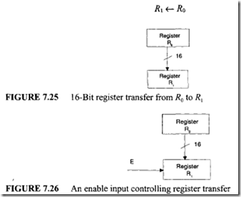
Register transfer notation is the fundamental concept associated with the control unit design. For example, consider the register transfer operation of Figure 7.25. The contents of 16-bit register R0 are transferred to 16-bit register R 1 as described by the following notation:
The symbol <— is called the transfer operator. However, this notation does not indicate the number of bits to be transferred. A declaration statement specifying the size of each register is used for the purpose:
Declare registers R0 [16], R1 [16]
The register transfer notation can also be used to move a specific bit from one
register to a particular bit position in another. For example, the statement
R 1 [1] <— R0 [14]
means that bit 14 of register R0 is moved to bit I of register R 1 •
An enable signal usually controls transfer of data from one register to another.
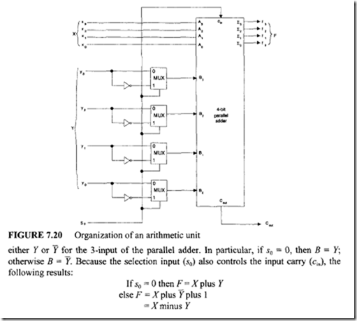
For example, consider Figure 7.26. In the figure, the 16-bit contents of register R0 are transferred to register R 1 if the enable input E is HIGH; otherwise the contents of R0 and R 1 remain the same. Such a conditional transfer can be represented as
E: R 1 <— R0
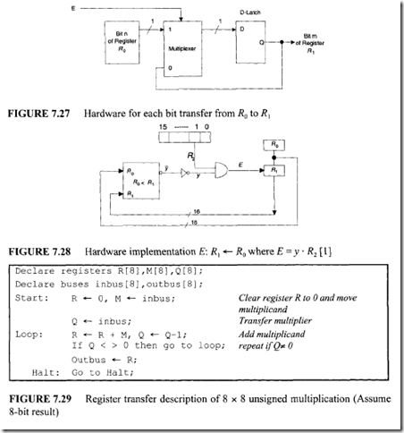
Figure 7.27 shows a hardware implementation of transfer of each bit of R0 and R 1 •
The enable input may sometimes be a function of more than one variable. For example,
consider the following statement involving three 16-bit registers: If R0 < R 1 and R2 [1] = I then R 1 <–– R0 •
The condition R0 < R 1 can be determined by an 8-bit comparator such that the output y of the comparator goes to 0 if R0 < R 1 • The conditional transfer can then be
expressed as follows: E: R1 <—- R0 where E= y ·R2 [1). Figure 7.28 depicts the hardware implementation.
A number of wires called "buses" are normally used to transfer data in and out of a digital processing system. Typically, there will be a pair of buses ("inbuses" and "outbuses") inside the CPU to transfer data from the external devises into the processing section and vice versa. Like the registers, these buses are also represented using register transfer notations and declaration statements. For example, "Declare inbus [16] and outbus [16]" indicate that the digital system contains two 16-bit wide data buses (inbus and outbus). R0 inbus means that the data on the inbus is transferred into register R0 when the next clock arrives. An equate(=) symbol can also be used in place of <— For example, "outbus = R 1 [15:8]" means that the high-order 8 bits of the 16-bit register R 1 are made available on the outbus for one clock period. An algorithm implemented by a digital system can be described by using a set of register transfer notations and typical control structures such as if-then and go to. For example, consider the description shown in Figure 7.29 for multiplying two 8-bit unsigned numbers (Multiplication of an 8-bit unsigned multiplier by an 8-bit multiplicand) using repeated addition.
The hardware components for the preceding description include an 8-bit inbus, an 8-bit outbus, an 8-bit parallel adder, and three 8-bit registers, R, M, and Q. This hardware performs unsigned multiplication by repeated addition. This is equivalent to unsigned multiplication performed by assembly language instruction.
A distinguishing feature of this description is to describe concurrent operations. For example, the operations R <— 0 and M <— inbus can be performed simultaneously. As a general rule, a comma is inserted between operations that can be executed concurrently. On the other hand, a semicolon between two transfer operations indicates that they must be performed serially. This restriction is primarily due to the data path provided in the hardware. For example, in the description, because there is only one input bus, the operations M +
inbus and Q <— inbus cannot be performed simultaneously. Rather, these two operations must be carried out serially. However, one of these operations may be overlapped with the operation R <— 0 because the operation does not use the inbus. The description also includes labels and comments to improve readability of the task description. Operations such as R <—0 and M <— inbus are called "micro-operations", because they can be completed in one clock cycle. In general, a computer instruction can be expressed as a sequence of micro operations.
The rate at which a microprocessor completes operations such as R<—R + M is determined by its bus structure inside the microprocessor chip. The cost of the microprocessor increases with the complexity of the bus structure. Three types of bus
structures are typically used: single-bus, two-bus, and three-bus architectures.
The simplest of all bus structures is the single-bus organization shown in Figure 7.30. At any time, data may be transferred between any two registers or between a register and the ALU. If the ALU requires two operands such as in response to an ADD instruction, the operands can only be transferred one at a time. In single-bus architecture, the bus must be multiplexed among various operands. Also, the ALU must have buffer registers to hold the transferred operand.
In Figure 7.30, an add operation such as R0 <— R 1 + R2 is completed in three clock cycles as follows:
-
First clock cycle: The contents of R 1 are moved to buffer register B 1 of the ALU. Second
-
clock cycle: The contents of R2 are moved to buffer register B2 of the ALU.
-
Third clock cycle: The sum generated by the ALU is loaded into R0•
A single-bus structure slows down the speed of instruction execution even though data may already be in the microprocessor registers. The instruction’s execution time is longer if the operands are in memory; two clock cycles may be required to retrieve the operands into the microprocessor registers from external memory.
To execute an instruction such as ADD between two operands already in register, the control logic in a single-bus structure must follow a three-step sequence. Each step represents a control state. Therefore, a single-bus architecture requires a large number of states in the control logic, so more hardware may be needed to design the control unit. Because all data transfers take place through the same bus one at a time, the design effort to build the control logic is greatly reduced.
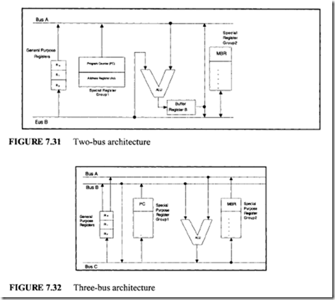
Next, consider a two-bus architecture, shown in Figure 7.31. All general-purpose registers are connected to both buses (bus A and bus B) to form a two-bus architecture. The two operands required by the ALU are, therefore, routed in one clock cycle. Instruction execution is faster because the ALU does not have to wait for the second operand, unlike the single-bus architecture. The information on a bus may be from a general-purpose register or a special-purpose register. In this arrangement, special-purpose registers are often divided into two groups. Each group is connected to one of the buses. Data from two special-purpose registers of the same group cannot be transferred to the ALU at the same time.
In the two-bus architecture, the contents of the program counter are always transferred to the right input of the ALU because it is connected to bus A. Similarly, the contents of the special register MBR (memory buffer register, to hold up data retrieved from external memory) are always transferred to the left input of the ALU because it is connected to bus B.
In Figure 7.31, an add operation such as R0 o(- R 1 + R2 is completed in two clock cycles as follows:
-
First clock cycle: Second clock cycle: The contents of R 1 and R2 are moved to the inputs of ALU.
-
The ALU then generates the sum in the output register. The sum from the output register is routed to R0•
The performance of a two-bus architecture can be improved by adding a third bus (bus C), at the output of the ALU. Figure 7.32 depicts a typical three-bus architecture. The three-bus architecture perform the addition operation R0 o(- R 1 + R2 in one cycle as follows:
-
First cycle: The contents of R 1 and R2 are moved to the inputs of the ALU via bus A and bus B respectively. The sum generated by the ALU is then transferred to R0 via bus C.
The addition of the third bus will increase the system cost and also the complexity of the control unit design.
Note that the bus architectures described so far are inside the microprocessor chip. On the other hand, the system bus connecting the microprocessor, memory, and I/O are external to the microprocessor.
Another important concept required in the design of a control unit is the generation of timing signals. One of the main tasks of a control unit is to properly sequence a set of operations such as a sequence of n consecutive clock pulses. To carry out an operation, timing signals are generated from a master clock. Figure 7.33 shows the input clock pulse and the four timing signals T0, T1 , T2 , and T3 • A ring counter (described in Chapter 5) can be used to generate these timing signals. To carry out an operation Pi at the ith clock pulse, a control unit must count the clock pulses and produce a timing signal Ti.
Hardwired Control Design
The steps involved in hardwired control design are summarized as follows:
1. Derive a flowchart from the problem definition and validate the algorithm by using trial data.
2. Obtain a register transfer description of the algorithm from the flowchart.
3. Specify a processing hardware along with various components.
4. Complete the design of the processing section by establishing the necessary control inputs.
5. Determine a block diagram of the controller.
6. Obtain the state diagram of the controller.
7. Specify the characteristic of the hardware for generating the required timing signals used in the controller.
8. Draw the logic circuit of the controller.
The following example is provided to illustrate the concepts associated with implementation of a typical instruction in a control unit using hardwired control. The unsigned multiplication by repeated addition discussed earlier is used for this purpose. A 4-
bit by 4-bit unsigned multiplication will be considered. Assume the result of multiplication is 4 bits.
Step 1: Derive a flowchart from the problem definition and then validate the algorithm using trial data.
Figure 7.34 shows the flowchart. In the figure, M and Q are two 4-bit registers containing the unsigned multiplicand and unsigned multiplier respectively. Assume that the result of multiplication is 4-bit wide. The 4-bit result of the multiplication called the "product" will be stored in the 4-bit register, R. The contents of R are then output to the outbus.
The flowchart in Figure 7.34 is similar to an ASM chart and provides a hardware description of the algorithm. The sequence of events and their timing relationships are described in the flowchart. For example, the operations, R E <— 0 and M <— multiplicand shown in the same block are executed simultaneously. Note that M <— multiplicand via inbus and Q <— multiplier via inbus must be performed serially because both operations use a single input bus for loading data. These operations are, therefore, shown in different
blocks. Because R<— 0 does not use the inbus, this operation is overlapped, in our case, with initializing of M via the inbus. This simultaneous operation is indicated by placing them in the same block.
The algorithm will now be verified by means of a numerical example as shown in Figure 7.35. Suppose M = 01002 = 410 and Q = 00112 = 310; then R =product= 11002 = 1210
Step 2: Obtain a register transfer description of the algorithm from the flowchart. Figure 7.36 shows the description of the algorithm.
Step 3: Specify a processing hardware along with various components. The processing section contains three main components:
-
General-purpose registers
-
4-bit adder
-
Tristate buffer
Figure 7.37 shows these components. The general-purpose register is a trailing edge-triggered device.
Three operations (clear, parallel load, and decrement) can be performed by applying the appropriate inputs at C, L, and D. All these operations are synchronized at the trailing (high to low) edge of the clock pulse.
The 4-bit adder can be implemented using 4-bit adder circuits. The tristate buffer is used to control data transfer to the outbus.
Step 4: Complete the design of the processing section by establishing the necessary control inputs.
Figure 7.38 shows the detailed logic diagram of the processing section, along with the control inputs.
Step 5: Determine a block diagram of the controller. Figure 7.39 shows the block diagram.
The controller has three inputs and seven outputs. The Reset input is an asynchronous input used to reset the controller so that a new computation can begin. The Clock input is used to synchronize the controller’s action. All activities are assumed to be synchronized with the trailing edge of the clock pulse.
Step 6: Obtain the state diagram of the controller.
The controller must initiate a set of operations in a specified sequence. Therefore, it is modeled as a sequential circuit. The state diagram of the unsigned multiplier controller is shown in Figure 7.40.
Initially, the controller is in state T0• At this point, the control signals C0 and C1 are HIGH. Operations R 0 and M inbus are carried out with the trailing edge of the next clock pulse. The controller moves to state T1 with this clock pulse. When the controller is
in T2, R <— R + M and Q <— Q – 1 are performed.
All these operations take place at the trailing edge of the next clock pulse. The controller moves to state T5 only when the unsigned multiplication is completed. The controller then stays in this state forever. A hardware reset input causes the controller to move to state T0, and a new computation will start.
In this state diagram, selection of states is made according to the following guidelines:
If the operations are independent of each other and can be completed within one clock cycle, they are grouped within one control state. For example, in Figure 7.40, operations R 0 and M ,. inbus are independent of each other. With this hardware, they can be executed in one clock cycle. That is, they are
microoperations. However, if they cannot be completed within the T0 clock cycle, either clock duration must be increased or the operations should be divided into a sequence of microoperations.
-
Conditional testing normally implies the introduction of new states. For example, in the figure, conditional testing of Z introduces the new state T3 •
-
One should not attempt to minimize the number of states. When in doubt, new states must be introduced. The correctness of the control logic is more important than the cost of the circuit.
Step 7: Specify the characteristics of the hardware for generating the required timing signals.
There are six states in the controller state diagram. Six nonoverlapping timing signals (T0 through T5) must be generated so that only one will be high for a clock pulse. For example, Figure 7.41 shows the four timing signals T0, T1, T2,and T3 • A mod-8 counter and a 3-to-8 decoder can be used to accomplish this task. Figure 7.42 shows the mod-8 counter.
Step 8: Draw the logic circuit of the controller.
Figure 7.43 shows the logic circuit of the controller. The key element of the implementation in Figure 7.43 is the sequence controller (SC) hardware, which sequences
![image_thumb[9] image_thumb[9]](http://lh4.ggpht.com/-D8bumeRZ500/VI8IZkAWuSI/AAAAAAAA8Uc/_9X2q4_5YXw/image_thumb%25255B9%25255D_thumb.png?imgmax=800) the controller according to the state diagram of Figure 7.40. Figure 7.44(a) shows the truth table for the SC controller.
the controller according to the state diagram of Figure 7.40. Figure 7.44(a) shows the truth table for the SC controller.
Consider the logic involved in deriving the entries of the SC truth table. The mod- 8 counter is loaded (or initialized) with the specified external data if the counter control inputs C and L are 0 and I respectively from Figure 7.42. In this counter, the counter load control input L overrides the counter enable control input E.
From the controller’s state diagram of Figure 7.40, the controller counts up automatically in response to the next clock pulse when the counter load control input L = 0 because the enable input E is tied to HIGH. Such normal sequencing activity is desirable for the following situations:
-
Present control state is T0, T1 , T2, T4 •
-
Present control state is T3 and Z = 1; the next state is T4 •
-
The SC must load the counter with the appropriate count when the counter is required to load the count out of its normal sequence.
For example, from the controller’s state diagram of Figure 7.40, if the present control state is T3 (counter output O2O1O0= 011) and if Z = 0, the next state is T2• When these input conditions occur, the counter must be loaded with external value 010 at the trailing edge of the next clock pulse (T2 = I only when O2O1O0= 010. Therefore, the SC generates L = 1 and d2d1d0= 010.
Similarly, from the controller’s state diagram of Figure 7.40, if the present state is T5 , the next control state is also T5 • The SC must generate the outputs L = 1 and dAdo = 101. The SC truth table of Figure 7.41 shows these out-of-sequence counts. For each row of the SC truth table of Figure 7.44(a), a product term is generated in the PLA:
P0 + ZT3 and P, = T5 •
The PLA (Figure 7.44b) generates four outputs: L, d2, d,, and d0• Each output is directly generated by the SC truth table and the product terms. The PLA outputs are as follows: ![image_thumb[10] image_thumb[10]](http://lh5.ggpht.com/-V1VFQkOVkoM/VI8Icvb3NwI/AAAAAAAA8Us/KkNqeA3u8fY/image_thumb%25255B10%25255D_thumb.png?imgmax=800)
From these equations, when the control is in state T0 or T2 , multiple micro operations are performed. Otherwise,when the control is in state T, or T4, a single micro operation is performed.
The unsigned multiplication algorithm just implemented using hardwired control can be considered as an unsigned multiplication instruction with a microprocessor. To execute this instruction, the microcomputer will read (fetch) this multiplication instruction from external memory into the instruction register located inside the microprocessor. The contents of this instruction register will be input to the control unit for execution. The control unit will generate the control signals C0 through C6 as shown in Figure 7.43. These control signals will then be applied to the appropriate components of the processing section in Figure 7.38 at the proper instants of time shown in Figure 7.40. Note that the control signals are physically connected to the hardware elements of Figure 7.38. Thus, the execution of the unsigned multiplication instruction will be completed by the microprocessor.
![image_thumb[1] image_thumb[1]](http://lh3.ggpht.com/-7vzW76NvbI8/VI8H5WgCjFI/AAAAAAAA8Sc/RJRpGnamLz8/image_thumb%25255B1%25255D_thumb.png?imgmax=800)
![image_thumb[2] image_thumb[2]](http://lh6.ggpht.com/-sv8bw9qeJ8s/VI8H8UpFuqI/AAAAAAAA8Ss/I7LzXSxcz-I/image_thumb%25255B2%25255D_thumb.png?imgmax=800)
![image_thumb[3] image_thumb[3]](http://lh4.ggpht.com/-_DjNmmoC72Q/VI8IAcKnVGI/AAAAAAAA8S8/ZlJUjrj-APk/image_thumb%25255B3%25255D_thumb.png?imgmax=800)
![image_thumb[4] image_thumb[4]](http://lh3.ggpht.com/-mlC44ycrNL4/VI8IDndxS2I/AAAAAAAA8TM/ixMNVthTTvE/image_thumb%25255B4%25255D_thumb.png?imgmax=800)
![image_thumb[5] image_thumb[5]](http://lh6.ggpht.com/-yuuLpC0Gtgc/VI8IG0tz9WI/AAAAAAAA8Tc/Rzav4YkjYv4/image_thumb%25255B5%25255D_thumb.png?imgmax=800)
![image_thumb[6] image_thumb[6]](http://lh3.ggpht.com/-vsEwAfisvDc/VI8IJz3YqVI/AAAAAAAA8Ts/J-MtUxsEaO8/image_thumb%25255B6%25255D_thumb.png?imgmax=800)
![image_thumb[7] image_thumb[7]](http://lh5.ggpht.com/-QKomt_BeIJA/VI8IS2AOjlI/AAAAAAAA8T8/1KY1IFo8Vss/image_thumb%25255B7%25255D_thumb.png?imgmax=800)
![image_thumb[8] image_thumb[8]](http://lh3.ggpht.com/-XqzG1b9oyKU/VI8IWE9LvKI/AAAAAAAA8UM/i41241CAB34/image_thumb%25255B8%25255D_thumb.png?imgmax=800)