Oscillators
In the introduction to the previous chapter of this book, I presented you with a simple block diagram of a ‘‘complete’’ digital electronic device: the digital clock. This device has all three of the necessary components for a functional, ‘‘stand alone’’ device: combinatorial logic for converting binary data as required; a memory function which ‘‘remembers’’ the last state it was in; and a clock or ‘‘oscillator’’ which synchronizes the functions together. The science of oscillator design is extremely rich and, as I will show in this chapter, there are a lot of options that you can choose from to make sure your application operates most efficiently.
It could also be argued that there is a fourth component to producing a complete, stand alone digital device – the power supply. Power supply design is a facet of electronics which is just as rich and sophisticated as digital electronics or any other major study in electronics. While I introduce you to some of the basic types of power supplies that are available to you later in the book, this does little more than just scratch the surface of this complex topic.
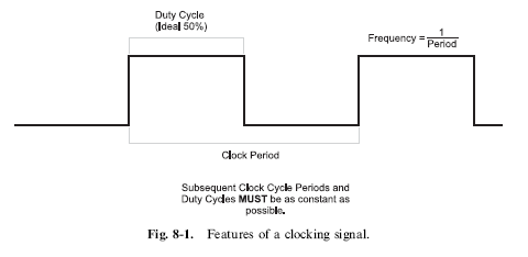
The application’s ‘‘clock’’ is a set of repeating pulses (ideally with the same ‘‘on’’ and ‘‘off’’ time) which is input into the sequential circuits of an application to carry out the operations within them. Figure 8-1 shows an ideal digital electronic clock waveform with the important features marked
on it. The frequency output of a clock is measured in ‘‘hertz’’ (cycles per second), which is the reciprocal of the time the pulse is on added to the time the pulse is off:
A rather obvious example of this would be a 1 pulse per second signal that is used to drive the sequential circuits of a timekeeping clock. The term ‘‘clock’’ is probably confusing, as the digital ‘‘clock’’ that I have defined is only very rarely used to tell the time. The clock signal that I am discussing in this section is used to drive the digital counters of the timepiece.
The ‘‘clock’’ in a digital circuit is driven from an ‘‘oscillator’’ that uses some form of feedback to toggle the clock line in a consistent manner. In this book, you will find that I use the terms ‘‘clock’’ and ‘‘oscillator’’ interchangeably, with the clock or oscillator signal being responsible for the operation of the digital circuit.
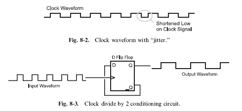
In Fig. 8-1, I noted the important features of a clock signal to be its constant period as well as its 50% duty cycle. If the clock is not constant and you were to look at the operation of the clock and the digital circuit on an oscilloscope, you would see the signals blur as they ‘‘jittered’’ back and forth. The shortened or lengthened features of a clock waveform are called ‘‘jitter’’ and are shown in Fig. 8-2. Jitter is a problem from a couple of perspectives. First, it makes it very difficult to observe the operation of a circuit using an oscilloscope, making it hard to debug an application. Secondly, the combinatorial logic parts of sequential circuits are often designed to have completed their bit data processing by the time the clock has completed; a shortened clock cycle, like the one shown in Fig. 8-2 could result in incorrect data being stored in a circuit.
Incorrect logic operation caused by jitter is extremely difficult to capture on an oscilloscope or a logic analyzer. If you have errors and have a clock with jitter, you would be well advised to assume that the jitter is the problem and look towards another clocking scheme. Jitter is often caused by voltage transients caused by different parts of a digital electronic circuit changing state; often it can be reduced or eliminated by providing better noise filtering between the oscillator circuit and the digital logic devices.
In Fig. 8-1, I indicated that the ideal ‘‘duty cycle’’ of a clock signal is 50%. I will discuss duty cycles in more detail later in the book when I present PWMs, but for now, you should understand that the duty cycle is the percentage of the period in which the waveform is high. Ideally, the clock should have a 50% duty cycle (be high for half the period) to minimize harmonics, simplify using an oscilloscope or logic analyzer to observe the operation of the circuit and, because some digital electronic devices (most notably microprocessors) poll both the high and low of the clock signal, to help speed up its operation.
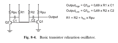
In some oscillator circuit designs, the output does not come close to having a 50% duty cycle and in these cases, some kind of signal ‘‘conditioning’’ is required. The most basic way of ensuring the clock signal has a 50% duty cycle is to use an edge triggered D flip flop as I show in Fig. 8-3. The D flip flop (called a ‘‘toggle flip flop’’ when wired this way) will only change its output when a triggering edge on the input clock has been received. The only drawback to this circuit is that it halves the frequency of the clock, so, in some cases, to use this circuit you will have to double the clock output frequency.
There are many different designs of oscillators that you can choose from. In this chapter I will introduce you to many of the most common ones along with their characteristics and the formulas required to work with them.
Transistor Astable Oscillators
When I was growing up, all educational and hobbyist circuits were built up from individual transistors – it wasn’t until the mid to late 1970s that ‘‘building block’’ chips such as the 555, LM339, LM386, and LM741 started to be commonly used in circuits. These chips are all very configurable, but none offer the range of operation and low cost of discrete transistors. The term ‘‘astable’’ indicates that the oscillator circuit is never stable; its output will continue to switch from high to low and back again. The science of oscillators can be thought of as ‘‘taming’’ the oscillator in terms of frequency, duty cycle and jitter.
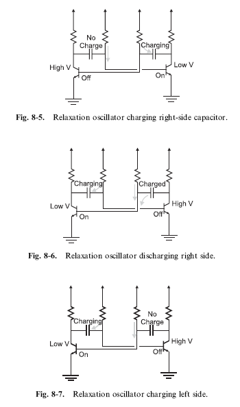
A very common and relatively simple oscillator circuit that I am going to examine is the basic ‘‘relaxation oscillator’’ circuit shown in Fig. 8-4. Included in Fig. 8-4 are the defining formulas for the time that the output is high and low as well as an important formula indicating that the value of R1 and R2 (the time defining resistors) must be the transistor hFE multiplied by the value of the pull up resistors (Rpu). If R1 or R2 is less than this product, then you will find that the oscillator will not start reliably and not run at a constant frequency.
The operation of the relaxation oscillator is illustrated in Figs. 8.5 through 8.7. In Fig. 8-5, I show an initial condition where one transistor is on and the other is off. In this case, the capacitor by the on transistor is chrging because its cathode is being pulled to ground by the ‘‘on’’ transistor. The other capacitor is unable to be charged because the transistor connected to its cathode is off, holding the voltage at the cathode at the same voltage as the anode.
In Fig. 8-6, the capacitor that was charging in Fig. 8-5 has finished and any current passing through the resistor is passed to the other transistor, turning it on. By turning on this transistor, the capacitor’s cathode connected to its collector is now tied to ground and it is able to be charged. With this capacitor now charging, the current that was once available to the
transistor’s base to turn it on is no longer available and the transistor turns off. This raises the collector of this transistor to the applied voltage and, along with this, the cathode of the capacitor connected to it. This places the charge in the capacitor tied to the collector of the transistor just turned off at a voltage higher than the applied voltage, so its charge is now passed to the transistor that was just turned on. In the final case (Fig. 8-7), the operation of
 the oscillator circuit is the mirror image of the initial conditions shown in Fig. 8-5. When the charging capacitor is finished, its current is passed to the transistor that is currently turned off and the process repeats itself.
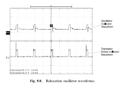
The output of this oscillator is probably nothing that you would expect – Fig. 8-8 is an oscilloscope display of a sample NPN transistor relaxation oscillator output as well as the collector voltage. The duty cycle of the waveform is nowhere close to 50% (which means it will have to be conditioned by some kind of circuit, like the one in Fig. 8-3. However, this circuit is quite good in terms of accuracy, with very little jitter.
The drawbacks to using a transistor oscillator like the one presented in this section include the unusual waveform output and the use of discrete analog components for timing the oscillator. The unusual waveform output makes the need for some kind of signal condition mandatory when working with digital electronics and the use of analog components makes the frequency output quite imprecise. The characteristics of the transistor-based oscillator make it best suited for low-cost applications where clocking accurate to 20% is acceptable.
Ring Oscillators
In the previous chapter, I introduced the concept of ‘‘ring oscillators’’ as being a digital electronic device in which an inverted output signal is fed back
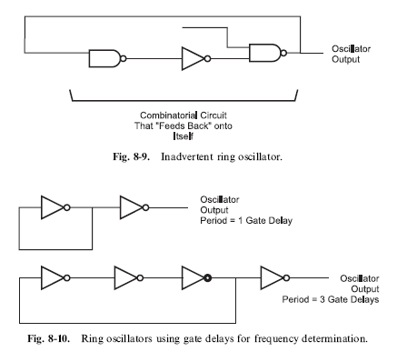
to the input of a combinatorial circuit and showed that it could be created inadvertently (Fig. 8-9) or purposely using a single logic inverter (Fig. 8-10). One of the useful characteristics of the ring oscillator is that it will always produce a 50% duty cycle and its output is literally the maximum speed of the technology.
I should say that the ring oscillator’s maximum output is the maximum speed of the technology. In Fig. 8-10, I have drawn two ring oscillators, the first outputting the signal from a single inverter – the period of the output of this circuit will be 1 gate delay. In the lower diagram of Fig. 8-10, I show that you are not limited to just running at the technology’s maximum speed; by adding an even number of additional inverters to the ring oscillator, the output signal’s period can be lengthened.
The ring oscillator’s actual frequency output can be ‘‘tuned’’ by varying the number of inverters in the ring oscillator along with the technology used in the inverters. Knowing this, along with a couple of operating rules, provides you with an inexpensive, high-speed oscillator that is quite reliable and robust.
 The first of the operating rules should not be surprising because I have alluded to it in the text above: the number of inverters in a ring oscillator should always be odd. If an even number of inverters is used in a ring oscillator, there will be no signal which cannot be resolved (which is the cause of the ‘‘astable’’ operation of an oscillator) and the circuit will not oscillate. The second operating rule is that no other functions should be used by the leftover gates in the chip and the chip’s power pins should have both small
(0.1 mF or less) and large (1.0 mF or greater) decoupling and filter capacitors on its power supply. The oscillating gates within the chip are experiencing significant transients which could affect the operation of other devices in the application.
While I have only used ring oscillators a couple of times over the years, they are fascinating circuits to build and watch executing. The ring oscillator is what I consider to be a ‘‘hip pocket’’ circuit: something to be pulled out only when nothing else seems to work or have the characteristics that you require.
Relaxation Oscillators
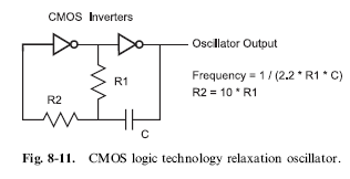
The most basic type of logic chip based oscillator is the ‘‘relaxation’’ oscillator which feeds back the output of an inverter through a ‘‘resistor/ capacitor’’ (‘‘RC’’) network to delay the switching of the oscillator. The basic circuit and its defining output equation is given in Fig. 8-11.
In this circuit, the R1 and C network are driven by the first inverter and the characteristic ‘‘RC’’ response is fed back to the first inverter’s input. When the voltage on the capacitor reaches the threshold voltage of the left inverter input, the inverter changes state and drives a new output voltage. This voltage is again passed through the R1, C network and delayed until the threshold voltage is reached again.
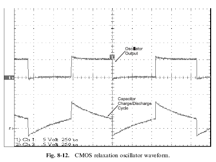 In Fig. 8-12, I have shown the voltage waveforms at the R1, R2 and C junction of this circuit as well as the output voltage signal. Note that the R1, R2 and C junction voltage exceeds the Vcc/Gnd (þ5 volts and 0.0 volt) limits. This is due to the capacitor being connected to the output driver.
Having the capacitor wired to the output driver ‘‘moves’’ the charge (and the capacitor voltage) by 5 volts each time the state changes. Observing the circuit’s operation from the capacitor, the output value changes the charge within the capacitor until it is back at the threshold voltage for the CMOS inverter, which is 2.5 volts (one-half applied power). You can see in Fig. 8-12 that the transitions take place every time the voltage across the capacitor is at 2.5 volts relative to Gnd.
CMOS inverters are used in this circuit because they are voltage controlled rather than current controlled and this makes the oscillator’s operation easier to understand. A TTL inverter cannot be used in this circuit because of the current drain operation required by the input when a ‘‘0’’ is input will affect the operation of the oscillator. A Schmidt trigger input device (i.e. the 74HC14) could be used, but it is not necessary because the reference voltage of the capacitor is changing with every transition.
You may want to test out this circuit with a 74C04 or 74HC04 with a 4.7 k resistor, a 47 k resistor and 0.1 mF capacitor to create an oscillator that produces a clock signal of approximately 1 kHz. I say that the output is
‘‘approximately’’ 1 kHz because of the tolerances of the parts used in the circuit. For the circuit used to produce the signal shown in Fig. 8-12, I used a
0.1 mF tantalum capacitor for the ‘‘C’’ in the relaxation oscillator circuit. This is probably not a ‘‘correct’’ use of a tantalum capacitor, as they can have tolerances approaching 30% of their rated value – I only used it because I have a lot of them around. Along with the tolerance of the capacitor, there are also the tolerances of the resistors in the circuit to consider as well. These tolerances result in the opportunity for the actual clock signal to be ‘‘out’’ by 40% or more.
Your immediate response may be to add a potentiometer (variable resistor) into the circuit and ‘‘tune’’ it to the exact frequency that you want. Personally, I would discourage this practice as it involves a lot of work (especially if production parts are involved), which will drive up the cost of the product. If you are using a simple RC relaxation oscillator in your application, then additional costs are something that you would want to avoid. The relaxation oscillator is adequate for many applications where a low-cost oscillator of an approximate value is required. Like the NPN transistor astable oscillator, I recommend that the circuit should not be used in any applications where any kind of precision is required.
Another aspect of this circuit that you must be aware of is the potential for
large current transients within the chip that are produced to change and discharge the capacitor. These transients are similar to the transients discussed in the ring oscillator. For most circuits, this is not a problem, but if you have other sensitive circuits built into an application, you will want to keep the relaxation oscillator (as well as any other oscillators in the circuit) as electrically removed as possible from the other chips by using both large and small decoupling and filtering capacitors. Also like in the ring oscillator, as a rule of thumb, no other gates should be used in a chip if it is being used as an oscillator.
