Crystals and Ceramic Resonators
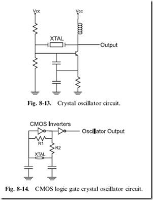
For the best clock accuracy, a quartz crystal should be used in an oscillator circuit like the one shown in Fig. 8-13. A quartz crystal is a piezoelectric device that provides a constant delay between one side of the piece of quartz within the part to the other. The term piezoelectric refers to the property of quartz (and some other compounds) to mechanically deform when a current is applied to it or produce a voltage potential when it is mechanically deformed.
In an oscillator, the quartz crystal will have a voltage applied to one end of it and this will cause the quartz crystal to deform. The rate at which this deformation takes place is known and will cause a voltage potential to be produced at the other end of the quartz crystal after a known delay. This voltage is used as a feedback value to an inverter built into the oscillator circuit. The NPN bipolar transistor-based inverter can be seen in Fig. 8-13.
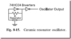
The circuit in Fig. 8-13 is somewhat ‘‘fiddly’’ to build and to get working reliably. There are some formulas that can be used to specify the different resistor, capacitor and inductor values, but, personally, I would never use this circuit in my own applications. This is why I did not put in any component values on the diagram; instead, I would use the inverter-based oscillator shown in Fig. 8-14. In this circuit, instead of understanding a circuit well enough to specify the correct different analog values, you can simply put a crystal across the input and output of a CMOS inverter.
The capacitors and resistors are necessary to ensure that the oscillator runs reliably and there are not any large over- or under-voltage spikes (caused by the operation of the piezoelectric producing its own voltage output). For most MHz range oscillator circuits, 15–33 pF capacitors are
adequate, 1–10 MQ for R1 and 100 to 100 kQ for R2 is appropriate. You may find that depending on the frequency of the crystal that you choose and how it is wired, you may have to vary these parts.
The second inverter in the circuit is not ‘‘strictly’’ required, but I like to have it in place to ensure the crystal is not ‘‘loaded down’’ by other devices and the operation of the oscillator doesn’t change. Any large loads on the output side of the oscillator’s primary inverter will affect the amount of current/voltage available to the crystal to pass the signal to the other side (and the oscillator’s frequency will drop or the oscillator won’t work at all).
Changing the capacitance on the inverter output side of the primary inverter results in small (1–2%) changes to the output and to help ensure the absolutely correct frequency output is produced a variable capacitor is used in place of the fixed capacitors. I do not feel this is practical and the nominal 0.01% or less error rate of the crystal should be accepted. I realize that there are applications (like digital clocks) where these changes are critical, but for the most part you should not have to ‘‘tune’’ the oscillator for the application.
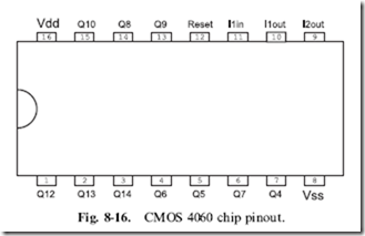
Crystals work quite well, although there are two drawbacks that you should be aware of. Crystals are relatively expensive parts (especially compared to the RC network relaxation oscillator). You can pay up to $10 for a crystal (although you can pay less than 1$ for common frequencies). In addition, the oscillator is somewhat ‘‘fragile’’ and can be easily damaged by rough handling. A relatively new device that can be used in place of a crystal
and does not have these shortcomings is the ‘‘ceramic resonator’’. A ceramic resonator is used in a very similar way to a quartz crystal (Fig. 8-15), but it is usually much less expensive and very rugged. I use ceramic resonators almost exclusively for clocking all my microcontroller applications. Despite the somewhat poorer accuracy of the parts (they are usually accurate to 0.5%), they really are the part of choice for most applications.
Many designers eschew the use of oscillators built from discrete parts as I have shown in this section. These circuits are rarely used because of the difficulty in specifying the correct parts for an application, the cost of the crystals and the potentially large amount of ‘‘real estate’’ that they can take up. Instead, oscillators are usually implemented using some kind of ‘‘canned’’
solution. These parts are designed to take up the same ‘‘footprint’’ as an eight or 14 pin ‘‘DIP’’ package and normally have four pins – power, ground, oscillator output and oscillator enable.
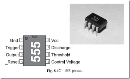
One of the most common chips used in digital logic applications is the CMOS 4060 (shown in Fig. 8-16). This chip can be used with the different oscillator types listed in this section and the ‘‘divide by’’ outputs are very handy in many circuits (often eliminating the need for separate counters).
The crystal, ceramic resonator and relaxation oscillator circuits that I have shown in this chapter can be used with this part. The ‘‘Q4’’ through ‘‘Q13’’ outputs are divided by counters (i.e. ‘‘Q4’’ is the clock divided by 2 to the 4 or 16 times).
When using the 4060, note that Pin 11 is the input to the inverter used in the oscillator circuits shown in this chapter, Pin 10 is output of the first inverter and input of the second inverter while Pin 9 is the output of the second inverter. If Pin 12 (‘‘Reset’’) is pulled high, the oscillator is stopped and the counters in the chip are reset.
555 Timer Chip
The 555 timer chip is probably the most versatile non-programmable part I have ever seen. Over the past 40 years, many people have created at least hundreds probably thousands of applications that have used this chip in ways I’m sure the original designer never would have thought possible; the original function of the chip was to provide a regular train of pulses. In this section, I will show how the chip is used in a circuit, along with some of the tricks that can be performed with it.
In the previous sections, I have shown you the ‘‘pinout’’ of a number of different components – each one of them having a unique form factor. The 555 is usually built into an eight pin ‘‘dual in-line package’’ that is commonly used for chips. In Fig. 8-17, I have put in an ‘‘overhead’’ view of the 555, along with a photograph of an actual 555 chip.
Looking at the labels for each of the pins, most of them do not make a lot of sense. What should jump out at you is the ‘‘Gnd’’ (ground) at Pin 1 and the ‘‘Vcc’’ (positive power) at Pin 8. These two pins are used to provide power for the part; they match the power pins I’ve presented elsewhere for digital devices elsewhere in the book.
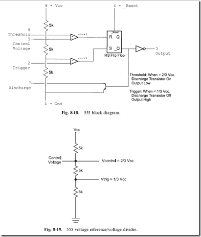
To try and get a better understanding of a chip, one of the first things I do is look for its block diagram and try to understand it. In Fig. 8-18, I have drawn out the block diagram for the 555 timer.
There should be two parts to the block diagram that you should recognize immediately. The first is the transistor at the bottom middle of the diagram.
This transistor is wired in an open collector configuration and is acting as a switch that will pass current to ground. The next piece that you should recognize is the voltage divider running along the left side of the block diagram that I have separated out into Fig. 8-19. If you were to work out the voltages at ‘‘Vcontrol’’ and ‘‘Vtrig’’, you would discover that they are at 2/3 Vcc and 1/3 Vcc, respectively. This is actually an important clue as to how the chip works.
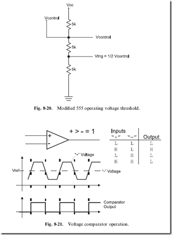
One aspect of the 555’s voltage divider circuit that you may find confusing is its connection to an outside pin called ‘‘Control Voltage’’. As I have shown in Fig. 8-20, this connection allows the circuit designer to change the voltage
levels of the voltage divider circuit. Rather than ‘‘Vcontrol’’ being 2/3 Vcc, it can now be any value (less than Vcc) that the designer would like. Changing ‘‘Vcontrol’’ also changes ‘‘Vtrig’’ to 1/2 ‘‘Vcontrol’’, as I have shown in Fig. 8-20.
The voltages at the ‘‘Vcontrol’’ and ‘‘Vtrig’’ are passed to two triangular boxes with a ‘‘+’’ and ‘‘ ’’ along with a funny looking equation. These boxes are representations for voltage ‘‘comparators’’ and, as I have shown in Fig. 8-21, the comparators output a high voltage level when the voltage at the ‘‘þ’’ input is greater than the voltage at the ‘‘ ’’ input. The 555 uses the two
comparators to continuously compare two external voltage levels to ‘‘Vcontrol’’ and ‘‘Vtrig’’ and pass the results to a box labeled ‘‘RS flip flop’’.
The 555’s RS flip flop saves an indication of which comparator last passed a high voltage to it. If the comparator connected to the ‘‘threshold’’
pin of the 555 and ‘‘Vcontrol’’ of the voltage divider output a high voltage, then the flip flop will output a high voltage at ‘‘_Q’’, which turns on the transistor at the bottom of the block diagram. If the other comparator passes a high voltage to the ‘‘RS flip/flop’’, then the voltage at ‘‘_Q’’ is driven low and the transistor is turned off. This is a fairly complete explanation of how the 555 works and I’m sure that you are at least as confused as you were when I first showed you the block diagram of the chip. The individual parts are quite easy to understand, but I’m sure you’re mystified how they work together.
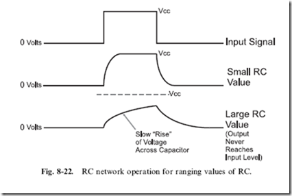
When I described the operation of the 555 chip, I neglected to take into account the components that would be wired to it. The timing delay
that is integral to the operation of the 555 is produced by resistors and capacitors wired in the ‘‘RC networks’’ that I have described earlier in the book. What I didn’t go into detail on in the previous sections of the book is that as you change the value of the resistor or capacitor in the circuit, you will change the delay produced by the two components (Fig. 8-22).
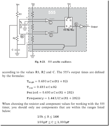
In Fig. 8-23, I have drawn a 555 oscillator circuit; when this circuit starts running, the 555 will be an ‘‘astable’’ oscillator with the output toggling,
The 0.01 mF capacitor wired to the ‘‘control voltage’’ pin of the 555 (in Fig. 8-23) is used as a ‘‘filter’’ for the internal voltages. This capacitor works very similarly to the logic circuit’s decoupling capacitor; if the input voltage changes, the capacitor will absorb or release charge to keep the voltage as even as possible.
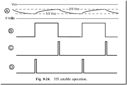
To get a better idea of how the 555 timer works as an oscillator, in
Fig. 8-23, I labeled the RC voltage (‘‘A’’), the RS flip flop output (‘‘B’’ – which is in the inverted 555 output), the ‘‘threshold’’ comparator voltage
(‘‘C’’) and the ‘‘trigger’’ comparator voltage (‘‘D’’). Figure 8-24 shows the waveforms for each of these parts marked in Fig. 8-23, so you can see the changing RC waveform, the output from the two comparators and the action of the RS flip flop.
Before going on, I want to share with you some of the more clever and useful circuits that have been created using the 555 timer. The few I will show in this chapter are just a small fraction of the number that is possible or has already been developed. If you are in a used book store, you should look for a copy of Don Lancaster’s ‘‘555 Timer Cookbook’’; it will really open your eyes to the incredible variety of applications this chip can help implement.
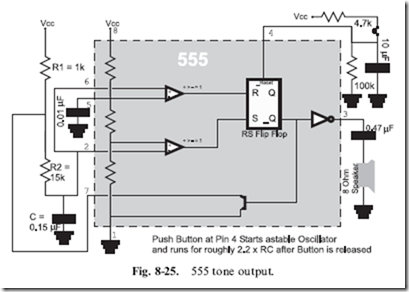
When stretching the envelope and using the 555 timer in a way that it wasn’t originally designed for, you generally look at the different input pins and see how they can be given a completely different function. If you wanted to make a circuit that drove out a tone for a set amount of time, you could use two cascaded 555 timers (or a single ‘‘556’’, which consists of two 555 timer chips in a single package) or the circuit shown in Fig. 8-25.
When this circuit is first turned on, the voltage at Pin 4 (the RS flip flop reset pin) is low, stopping the circuit from oscillating. When the momentary on button is pressed, current is passed to the 10 mF capacitor, charging it and driving up the voltage on Pin 4. This happens quite quickly and when Pin 4 reaches the logic threshold to stop holding the RS flip flop reset, then the 555 will start oscillating, driving out a signal that oscillates at 464 times per second.
This tone will stay on as long as the button is pressed and then will continue until the 10 mF capacitor discharges through the 100 k resistor. By varying the values for these two parts, you can vary the length of time the 555 continues to oscillate. Remember the rule of thumb that is used to approximate the time for an RC network, like this one, to discharge:
I take advantage of the ability of the human ear to distinguish between different sounds and categorize them with a circuit design for a continuity tester that you will probably find is a lot more useful than the simple instrument built into your digital multi-meter.
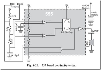
This continuity tester circuit shown in Fig. 8-26, is useful in a variety of different situations. Instead of just driving out a simple tone when an electrical path between the two probes has been found, it provides you with different tones and sounds, based on the resistance between the probes as well as an indication of whether or not a diode is between the probes. Because the circuit is self-powered, you can use it with circuits that are already working, without worrying about having a valid ground connection.
When there is no connection between the leads, the 5.1k resistor is part of the RC network that provides the delay for the 555 timer wired as an astable oscillator. With no connections, you will find that the oscillator outputs a tone that is at about 440 cycles per second (‘‘hertz’’ or ‘‘Hz’’). If there is a direct connection (or short circuit) between the two probes the 5.1 resistor is
not used in the delay and the frequency output is around 880 hertz, there is a full octave difference between the two signals.
What I like about this circuit is that you get a different frequency based on the resistance across the probes – the probe resistance is in parallel with the 5.1 k resistor, changing its frequency and the frequency output from it. This can be useful in finding ‘‘almost’’ short circuits such as a ‘‘just touching’’ connection rather than a hard soldered connection or a ‘‘high impedance short’’, when you expect no connection at all. In addition, try out a diode in a forward biased and reversed bias connection; you will be able to hear a noticeable difference here as well.
Delay Circuits
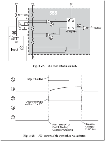
Another basic function of the 555 is use as a ‘‘monostable’’. In the previous section, I alluded to this function and noted that the 555 could do more than just be part of the ‘‘astable’’ oscillator which will run for ever – the monostable, on the other hand, will only execute once and requires triggering. The monostable is very useful for a variety of different applications and works similarly to digital logic chips that can provide a similar delay. Figure 8-27 shows the 555 wired as a monostable generator and Fig. 8-28 shows the response waveforms to the input pulse.
When the input goes low, the pulse output from the 555 timer is determined using the formula:
The 555’s RS flip flop is initially ‘‘reset’’, and the transistor that passes capacitor charge to ground is turned on. When the input (‘‘A’’) goes low and the ‘‘trigger’’ input receives a low voltage input, its comparator signal (‘‘E’’) goes
high, changing the state of the RS flip flop (‘‘C’’) and changing the state of the output pin. When the RS flip flop state changes again, the transistor is turned off and the capacitor charges through the resistor. The capacitor charges according to the formula:
until its voltage reaches 2/3 Vcc. When it reaches 2/3 Vcc, the ‘‘threshold’’ comparator (‘‘D’’) goes high and the RS flip flop changes state again, changing the value of the output pin (‘‘C’’). At this point, the 555 is back to its original state.
This circuit works quite well except for one point – the input pulse must always be shorter than the calculated output pulse. If the input pulse is longer than the calculated output pulse duration, you will find that the output will stay active, but it will pulse periodically. When the capacitor charges to 2/3 Vcc and the input is low down, both of the comparators will be driving a high voltage to the RS flip flop. This is an invalid condition for the RS flip flop and the output from the flip flop is ‘‘indeterminate’’, resulting in the transistor tying the capacitor to ground periodically. To avoid this behavior, you should always make sure that the length of time for the pulse output from the 555 is longer than the expected input.
Instead of using the 555 timer as a monostable delay generator, there are a number of logic chips that perform the same function using a resistor and capacitor. The 74123 incorporates two monostable delays that are programmed using a resistor and capacitor. The 74123 and other logic family chips have the advantage that the voltage level transitions do not cause as much disruption to the surrounding circuitry.
In some applications, there is a delay that is either more precise, shorter or longer than can be practically created using the RC-controlled monostables that I have presented so far. In the next chapter, I will be introducing you to ‘‘counters’’ which will either count continuously or stop when a specific value has been reached. The counter, driven by one of the oscillators presented in this chapter, is used to produce either a very long or very precise delay.
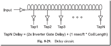
For shorter delays, there are two methods that you can consider. The first method is to use a ‘‘canned’’ delay line. These components usually consist of an inverting buffer, driving a long copper line. At different points along the line, inverting ‘‘taps’’ are put in place to drive out the signal. Figure 8-29 shows how these components are used.
When you see an actual ‘‘delay line’’ component, you will probably refer to it as a ‘‘chip’’. I hesitate to do so because I consider a chip to be simply a silicon chip bonded to a ‘‘lead frame’’ and ‘‘encapsulated’’ in some manner.
In a delay line component (or ‘‘module’’), the wire delay is wound in a coil
with the tap inverter inputs soldered to it at different intervals. The actual device requires ery high precision mechanical assembly (more than a standard plastic encapsulated chip) and any errors in assembly or encapsulation will result in a useless part.
The wire in the part passes the digital signal to the various taps within the part, with a delay of roughly 1 nanosecond per foot (30 cm) of wire. When you design high-speed applications, this rule of thumb is very important when you are designing high-speed digital electronic circuits. Chances are you will ask that the traces on PCBs are ‘‘routed’’ with 0.1 inch (2.54 mm) precision to ensure that parallel signals all ‘‘show up’’ at the same place at the same time in the high-speed application circuit.
The advantage of the delay line module is that timing delay can be very precise. Custom-made delay line modules are available (the manufacturer solders the taps at specified points in the coil rather than at standard positions), which can be critical in some applications. This high level of assembly/encapsulation precision has a price that you will have to pay. If you can buy a 74LS04 for less than a quarter in single units, you should not be surprised to discover that a delay line module will cost you over $10.00. The delay line provides you with the best control over different delays required in a circuit, but at quite a significant cost. Delay line modules should only be considered if no other options are available to you when you are designing a circuit.
Another method of delaying signals is to take advantage of the natural delays of digital electronic gates and simply ‘‘chain’’ a number of them together to get a needed delay. In Fig. 8-30, I have shown a 20, 40 and 60 nsec delay built out of a 74LS04 TTL chip.
The advantage of this method is that it is quite low cost and reasonable precision can be built into the circuit. When you are designing delays for your applications, you should consult with the technology operational characteristics chart that I provided earlier in the book (see Table 6-2).
Working with different technologies, you should be able to get quite accurate delays quite inexpensively. The disadvantage of this method is that
it can take up a lot of space on a board (at which point the canned delay line may have to be considered).
Quiz
1. An ideal digital electronic clock waveform has:
(a) A constant period with a 50% duty cycle
(b) A selectable speed range
(c) A period that is less than the gate delay of the logic technology being used with it
(d) A varying period that takes advantage of the operation of the combinatorial circuitry in the sequential circuit
2. Each of the following are important characteristics of astable oscillators except for
(a) Period
(b) Jitter
(c) Duty cycle
(d) Power required
3. If the R1 or R2 resistor values are less than the product of hFE and Rpu, the NPN transistor relaxation oscillator will:
(a) Not be reliable and may not start up
(b) Not work correctly
(c) Get very hot because the transistors are continuously in saturation
(d) Produce a perfect, 50% duty cycle output
4. The practice of putting ring oscillators in leftover gates:
(a) Helps minimize the cost of a digital electronics application
(b) Helps synchronize other gates in the chip
(c) Should only be done if there is an odd number of inverting gates left in the chip
(d) Should be strenuously discouraged
5. A relaxation oscillator has an R1 value of 10 k, C of 0.1 mF and R2 equal to 1 k. What frequency will it oscillate at?
(a) It won’t oscillate
(b) 4.54 kHz
(c) 4.54 MHz
(d) 4.54 Hz
6. What type of application is the relaxation oscillator best suited for?
(a) High power
(b) High cost, not requiring accurate operation
(c) Low cost, high accuracy
(d) Low cost, not requiring accurate operation
7. Canned oscillators are used because:
(a) They are more accurate than discrete component solutions
(b) They are cheaper than discrete oscillator solutions
(c) They are simple and accurate
(d) They are more reliable than discrete component solutions
8. The only type of oscillator that the 4060 cannot implement is:
(a) Ring oscillator
(b) Relaxation oscillator
(c) Crystal/ceramic resonator oscillator
(d) NPN transistor relaxation oscillator
9. Increasing the value of a resistor or capacitor in a 555 astable oscillator will:
(a) Lower its operating frequency
(b) Raise its operating frequency
(c) Increase the output voltage
(d) Lower the output voltage
10. Connecting six 74AS inverters (gate delay 2 ns) end to end will produce a delay circuit that is:
(a) 24 ns
(b) 12 ns
(c) 72 ns
(d) 48 ns
