USART 8251 (Universal Synchronous/ Asynchronous Receiver Transmitter)
1. Draw the pin diagram of USART 8251.
Ans. The pin diagram of 8251 is as shown below:
2. Draw the functional block diagram of 8251.
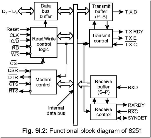
Ans. The functional block diagram of 8251 is shown below:
3. How many different sections does 8251 have?
Ans. 8251 has five sections: Read/Write control logic, data bus buffer, modem control, transmitter (including its control) and receiver (including its control).
4. How the 8251 is programmed?
Ans. 8251 is programmed by a 16-bit Control Word Register. This 16-bit register is divided into two bytes—the first byte corresponds to Mode Instruction Format while the second byte corresponds to Command Instruction Format. The content of control word register determines synchronous or asynchronous operation, Baud rate, number of bits per character, number of stop bits, nature of parity, etc.
5. What is the function of the Status Word Register of 8251?
Ans. The function of the status word register is to check or examine the preparedness of 8251 with regard to transmission or reception of data.
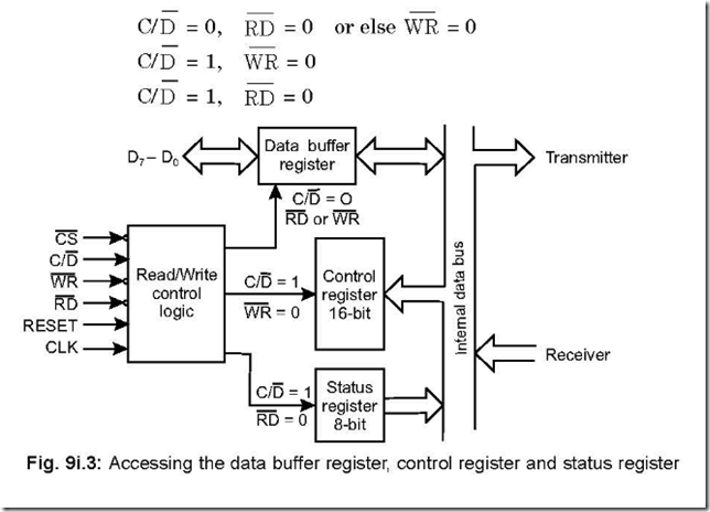
6. Describe the Read/Write Control logic and registers. Ans. It contains three buffer registers:
z data buffer register
z control register
z status register.
The six input signals are: CS , C/ D , WR, RD , RESET and CLK.
The particular 8251 is selected on CS signal going low. This pin is usually connected to a decoded address bus. C/ D stands for control/data pin. When this pin is high, either the control register or status register is selected and when low, data bus buffer is selected.
The control register and the status register are distinguished by WR and RD signals,
respectively.
The figure below shows how the three registers: data buffer register, control register
and status register are accessed by making respectively.
The following table shows the status of the control signals CS , C/ D , RD , WR for
accessing the different registers.
7.Explain the operation of the transmitter section of 8251.
Ans.
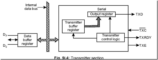
The transmitter section consists of three blocks—transmitter buffer register, output register and the transmitter control logic block. The CPU deposits (when TXRDY = 1, meaning that the transmitter buffer register is empty) data into the transmitter buffer register, which is subsequently put into the output register (when TXE = 1, meaning that the output buffer is empty). In the output register, the eight bit data is converted into serial form and comes out via TXD pin. The serial data bits are preceded by START bit and succeeded by STOP bit, which are known as framing bits. But this happens only if
![]()
![]() transmitter is enabled and the CTS is low. TXC signal is the transmitter clock signal which controls the bit rate on the TXD line (output line). This clock frequency can be 1, 16 or 64 times the baud.
transmitter is enabled and the CTS is low. TXC signal is the transmitter clock signal which controls the bit rate on the TXD line (output line). This clock frequency can be 1, 16 or 64 times the baud.
8. Explain the operation of the receiver section of 8251.
Ans.
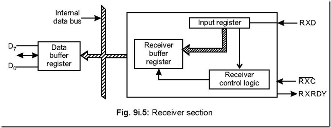
The receiver section consists of three blocks — receiver buffer register, input register and the receiver control logic block. Serial data from outside world is delivered to the input register via RXD line, which is subsequently put into parallel form and placed in the receiver buffer register. When this register is full, the RXRDY (receiver ready) line becomes high. This line is then used either to interrupt the MPU or to indicate its own status. MPU then accepts the data from the register.
![]() RXC line stands for receiver clock. This clock signal controls the rate at which bits are received by the input register. The clock can be set to 1, 16 or 64 times the baud in the asynchronous mode.
RXC line stands for receiver clock. This clock signal controls the rate at which bits are received by the input register. The clock can be set to 1, 16 or 64 times the baud in the asynchronous mode.
9. How does the CPU know that the transmitter buffer is empty?
Ans. The CPU knows about the same by
z examining the TXRDY line of the transmitter.
z examining D0 bit of the status word.
10. When the TxD line goes into the MARKING (HIGH) state? Ans. It becomes high in the following cases:
z a RESET is received by 8251.
z transmitter is empty.
z transmitter is not enabled.
z CTS is off.
11. How the transmitter is enabled?
Ans. The transmitter is enabled by setting bit D0 of the command instruction word.
12. What is the status of the start bit on the RXD line for 8251 (in asynchronous mode only) and how does it differentiate between a valid start pulse and transient pulse?
Ans. For any data to be received by the receiver, it first checks for a valid start bit which is zero. 8251 has an inbuilt false start bit detection circuit which can differentiate between an actual start bit pulse and a transient pulse.
13. What happens when a parity error or a framing error occurs in the received data bits (in asynchronous mode only)?
Ans. The Parity error and Framing error status bits in the status word are set if there is a parity error or if the stop bit is absent at the end of the received bits respectively.
14. When the RXRdy line goes high in asynchronous and synchronous mode of operation?
Ans. In the asynchronous mode, RXRdy line goes high
z if the receiver is in the enabled condition (this is made so by setting D2 bit of the Command Instruction Word).
z and after the receiver has detected a valid start bit, assembled the character bits and transferred the character to the receiver buffer register.
Whereas in the synchronous mode RXRdy line goes high
z if the receiver is enabled.
z a character is assembled and transferred to the receiver buffer register.
15. What is overrun error?
Ans. D4 bit of the status word stands for ‘over run error’.
If the CPU cannot read the data from the receiver buffer register (this happens if the
CPU fails to respond to RXRdy line), then on receipt of the next character, the previous data will be written over and the earlier character will be lost. When such is the case D4 bit of the status word is set.
16. Discuss the SYNDET/BD pin.
Ans. This is pin 16 of 8251 and stands for sync. detect (SYNDET)/Break Detect (BRKDET).
This pin is used for detection of SYNC characters in synchronous mode and Break characters in asynchronous mode.
Synchronous mode: In the synchronous case this pin (SYNDET) can be used as either input or output pin with the help of control word. When the system is RESET, the status of this pin is low in the output mode. When 8251 is programmed to receive two synchronous characters, this output pin goes high at the mid point of the last bit of the second synchronous character. The status of this pin can also be known by reading the status word, but gets resetted on STATUS READ.
In the input mode—called the external synchronous detect mode—a rising edge on this pin causes 8251 to start collecting data characters on the rising edge of the next RXC . This input signal can be removed once synchronisation is achieved. When external synchronisation is done, the internal synchronisation is disabled.
BRKDET: In this mode, this pin acts as an output pin to detect break characters. If RXD remains low for two consecutive stop bit sequences, this pin (BRKDET) goes high. Here also provision is there to read the status of this pin by STATUS READ operation.
This pin is reset
z on a Master Chip Reset
z when RXD becomes on 1.
17. What purpose does 8251 serve—DTE or DCE in a communication interface environment?
Ans. 8251 acts as a DTE (Data Terminal Equipment) in such a case.
18. Why modems (modulators-demodulators) are used in case of digital transmission of data?
Ans. The term ‘modem’ stands for modulator—demodulator. In a communication environment, two modems are used—one at the transmitting end side and one at the receiving end side. Modems are generally called DCE (Data Communication Equipment).
High frequency digital signals require a very wide transmission channel bandwidth which makes the system very costly. However, existing telephone line facilities (which carry analog signals in the range of 40 Hz to 4 KHz) can be used to transmit such high frequency digital signals. A modem converts a digital signal into audio tone frequencies (at the transmitting end side) and reconverts this audio frequencies into h.f. digital signals (at the receiving end side)—and it utilises Frequency Shift Keying (FSK) for this purpose. Thus a modem converts a logical ‘1’ to 1200 Hz and ‘0’ to 2200 Hz audio frequency. These signals are then transmitted over a telephone line over a ‘carrier’. The inverse operation is done at the receiving end side.
158 Understanding 808518086 Microprocessors and Peripheral /Cs through Questions and Answers
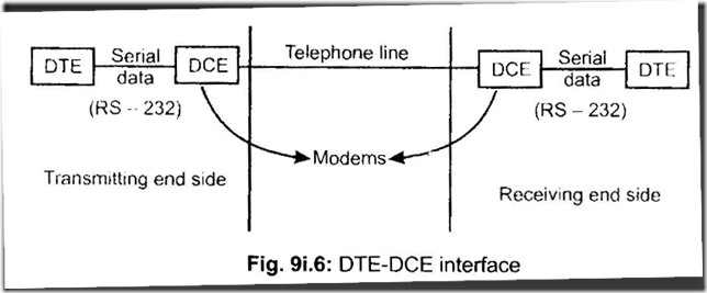
19. Draw the block diagram of a DTE-DCE interface in a communication environment.
Ans. The block diagram is shown below:
Digital data is delivered at the DTE (may be 8251) in parallel form, which is then converted into serial form and sent to DCE via RS-232 cable. The DCE (a modem) output is an audio signal carried through a telephone line.
At the receiving end side, the opposite process is carried out to retrieve the original data.
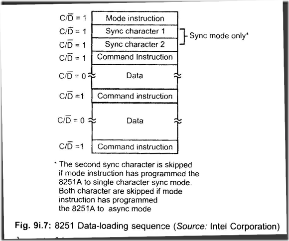
20. Draw the 8251 data loading sequence and explain the same.
Ans. The data loading sequence of 8251 is shown below:
The mode control is specified first, which indicates the general operating conditions. If the mode word indicates that it is a synchronous operation, then the synchronous character(s) is/are loaded. This is followed by loading the command instruction format.
In all these, C/ D = 1. After this, C/ D is made 0 when data is either transmitted/received.
It is followed by command instruction and data in that order which is repeated all over again.
A command word with D6 = 1returns 8251 to mode instruction format.
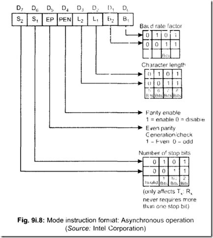
21. Discuss the mode instruction format for asynchronous transmission/reception case.
Ans. The mode instruction format for asynch ronous (transmission/reception) is shown below:
Bits D0D 1 cannot both be low for asynchronous communication. These two bits determine the baud rate factor. Bits D2 D3 determine the character length (which may be 5 to 8 bits in length)-depending on the content of the se two bits. Bit D4 stands for ‘Parity Enable’ (PEN) and is enabled if D 1 = 1 and otwrwise if D1 = 0. D:, bit stands for ‘Even Parity’ (EPl. Parity is even if D;; = 1 and odd il D,, = 0. Bits D6 and D7 determine
the number of stop bits. There can be 1, 1 y . 2 numb•’r of stop bits.
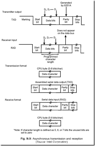
22. Draw the general transmission/receive format for asynchronous communication. Ans. The general transmission/receive format for asynchronous communication is shown below: The transmission format consists of start bit, data character, parity bit, stop bit(s)
in that order.
8251 starts sending data on the TXD (transmit data pin) pin with a start bit which is a 1to 0 transmission. Then the data bits are transmitted, followed by stop bit(s). The data bits start with LSB of the serial output register. All these bits (start bit, data bits,
stop bit(s) are shifted out on the falling edge of TXC (transmitter clock). In case when no data is transmitted, TXD output remains high. But if a ‘break’ is programmed, TXD line will go low.
The receive format is identical to transmit format. Data reception starts with RXD (receive data pin) line going low—it indicates the arrival of start bit. This 1 to 0 transition on the RXD line triggers the ‘False Start Bit Detection Circuit’. This circuit then samples the RXD line half-a-bit time later to ensure the presence of a genuine start bit. If this sampling results in a low on RXD line, it indicates a valid start bit. The bit counter is started on the second sampling—hence each subsequent data bit is
sampled at the middle of each bit period. This is called ‘mid bit sampling’. The bit counter thus samples the data bits, parity bit and lastly the stop bit. The receiver needs only one stop bit—but the transmitter is affected by the number of stop bits. For any error during receiving of data with regard to Parity, Framing or Overrun—the corresponding flags in the status word are set.
23. Why the ‘false start bit detection circuit’ is there in asynchronous reception case?
Ans. This is done to avoid any possibility of a false start bit detection due to a transient noise pulse.
24. Discuss the mode instruction format for synchronous transmission/reception case.
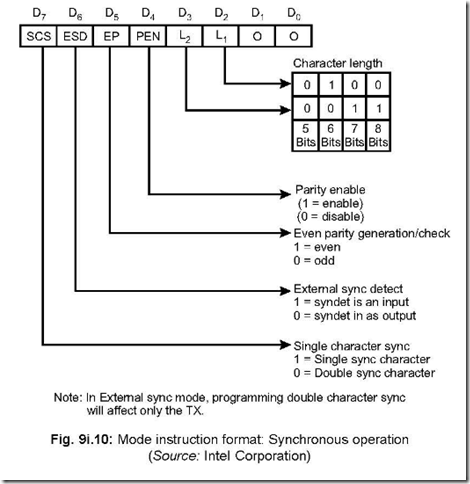
Ans. The mode instruction format for synchronous operation (transmission/reception) is shown below:
Bits D0 D1 both will have to be low for synchronous transmission/reception of data. Bits D2 D3 indicates the character length. Bits D4 and D5 stand for PEN and EP respectively—exactly same as in the case of asynchronous case. Bit D6 stands for ESD (External Synchronous Detect). D6 = 1 stands for input and D6 = 0 stands for output. Bit D7 stands for SCS (Single Character Sync.) with D7 = 1 indicating a single synchronous character and D7 = 0 indicating double synchronous characters.
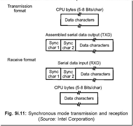
25. Draw the general transmission/receive format for synchronous communication. Ans. The general transmission/receive format for synchronous communication is shown below.
![]() In the transmission format, either one or two synchronous characters are sent, followed by data characters. The number of synchronous characters (i.e., 1 or 2) is previously decided by the bit D6 in the mode instruction format for synchronous operation. For such communication to take place, C/ D will have to be 1. The characters are shifted out of the serial output register on the falling edge of the TXC (transmitter clock), and at the same rate as the TX C . Once transmission commences, it is the duty of the CPU to replenish the transmitter buffer register in response to TXRdy. If the CPU fails to provide a character before the transmitter buffer becomes empty, 8251 automatically sends SYNC character(s). In such a case, TXE (Transmitter Empty) pin becomes high to indicate that the transmitter buffer is empty.
In the transmission format, either one or two synchronous characters are sent, followed by data characters. The number of synchronous characters (i.e., 1 or 2) is previously decided by the bit D6 in the mode instruction format for synchronous operation. For such communication to take place, C/ D will have to be 1. The characters are shifted out of the serial output register on the falling edge of the TXC (transmitter clock), and at the same rate as the TX C . Once transmission commences, it is the duty of the CPU to replenish the transmitter buffer register in response to TXRdy. If the CPU fails to provide a character before the transmitter buffer becomes empty, 8251 automatically sends SYNC character(s). In such a case, TXE (Transmitter Empty) pin becomes high to indicate that the transmitter buffer is empty.
In the receive format, C/ D is maintained at high level. In the internal SYNC mode, the receiver samples the data available as the RXD pin on the rising edge of RX C . The command word should be previously programmed with the ‘ENTER HUNT’ command (bit D7 of the Command Instruction Format) in the Enabled Condition (D7 = 1). The receiver buffer register content is compared at every bit boundary with the SYNC character (previously loaded) till a match occurs. The process is extended to two SYNC characters if the 8251 is initially programmed for two SYNC characters (bit D7 of the Mode Instruction Format). After ‘HUNTING’ is over, the system goes for character boundary synchronisation so that it can assemble the serial data to be subsequently changed to parallel format. The SYNDET pin is set high, which can be ascertained with a status read. This is resetted once status read is over. The SYNDET pin gets set in the middle of the parity bit if the parity is enabled; otherwise in the middle of the last data bit. In the external SYNC mode, 8251 comes out of HUNT mode by a high level on the SYNDET pin, which acts as an input in such a case.
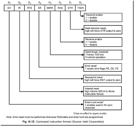
26. Show the Command Instruction Format and explain the same. Ans. The Command Instruction Format is shown below:
The command instruction format controls the functioning of 8251. A command word with D6 = 1 returns 8251 in mode instruction format. If D0 (TXEN) is mode high, data transmission is possible whereas making D2 (RXE) high, enables the system for reception. If D1 (DTR) is made high, the DTR output will be forced in the zero state. A high on D4 (ER) forces resetting of error flags PE, OE and FE (Parity, overrun and Framing errors respectively) in the status word. A high on D3 (SBRK) forces TXD low while a zero corresponds to normal operation.
27. What happens when (a) power is switched on (b) the system is resetted?
Ans. On powering on the system, 8251 either enters into SYNC or command instruction format.
On resetting the system, 8251 returns to the mode instruction format from the command instruction format.
28. Draw the status word format and explain the same.
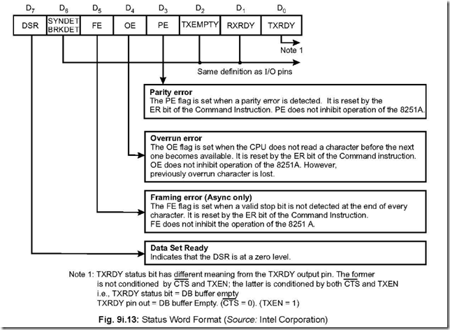
Ans. The status word format for 8251 is shown below
The status word can be read with C/ D = 1. The CPU, for its proper operation, needs various informations. These are provided by the status word. It should be borne in mind that the status word is continuously updated by 8251, but not while the CPU reads it.
29. What are the modem control pins associated with 8251? Describe the functioning of these pins.
Ans. The modem control section of 8251 are handled by these four pins: DSR , DTR , CTS and RTS . Out of these, the first and third are input pins (input to 8251) and the rest two are output pins. All these pins are active low. The signals on these pins are also used for purposes other than modem control. The description of these pins are given below:
DSR (Data Set Ready): This is a 1-bit inverting input port. It is used by the modem to signal the 8251 (here DTE) that it (modem) is ready to accept data for transmission. The DSR bit is checked by reading (polling) the D7 bit of the status word. If it is low, then the modem can send data to 8251.
DT R (Data Terminal Ready): This is a 1-bit inverting output port. It is used by 8251 to signal the modem about its readiness to accept/transmit data. D1 bit of command instruction word can either be set/reset, with a high D1 bit forcing DTR output to zero.
RTS (Request to Send): This is a 1-bit inverting output port. It is used by 8251 to signal the modem that it has data to send. Bit D5 of the Command Instruction Format controls the status of this pin.
CTS (Clear to Send): This is a 1-bit inverting input port. It is used by modem to signal 8251 that it has the right of way over the communication channel and can send out serial data. Bit D0 of the command instruction word should be enabled for the above to be realised.
If D0 is made low in command instruction word while data transmission is taking place or if CTS is switched off, the transmitter will complete sending the data stored in its buffer prior to getting disabled.
30. What is the baud rate of 8251?
Ans. The asynchronous baud rate of 8251 is 9600, while for the improved version of 8251— i.e., 8251A, this is 19, 200.
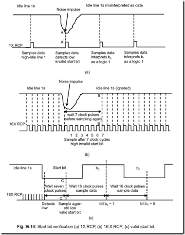
31. Discuss how a noise pulse may be recognised as a valid start pulse. How this possibility is eliminated?
Ans. In the asynchronous case, a USART may be programmed for receive clock rates of 8,16,32,64 times the receive data rate (these correspond to 8X, 16X, 32X and 64X). Thus the receive clock rates may be 8X RCP, 16X RCP, 32X RCP and 64X RCP, apart from the normal 1X RCP. Actually, 1X RCP corresponds to the receive data rate.
Fig. 9i.14(a) shows the situations when the line is idle (i.e., in state ‘1’) and is hit by
a noise impulse. The receive clock pulse (RCP) is set at 1X RCP. The figure shows the uneventful situation of the clock pulse sampling the input line at the instant the noise is present (point A A′ ) and the circuit detects a low. This gives rise to an invalid start bit and the subsequent clocks will interprete the high condition on the data line to be data bits—all at logic 1’s. This gives rise to a serious error arising out of an accidental noise pulse.
Fig. 9i.14(b) shows the same situation with the exception that the receiver clock is now made sixteen times faster—i.e., 16X RCP. Once a low is detected, the receiver is made to wait for seven clock cycles before it resamples the input data (this corresponds to BB′ in the fig.). Since in this case the receiver analyses the input line status to be ‘1’, hence it concludes that the low input line status that it detected seven clock cycles earlier to be a noise pulse. Thus the possibility of the UART receiver accepting spurious noise pulse is eliminated. This can further be improved by increasing the clock rate to 32X, 64X, etc.
Fig. 9i.14(c) shows the input line scanned by the same 16X RCP. It shows a valid start bit followed by data bits. As in Fig. (b), here also the receiver waits for seven clock cycles after detecting a low. Here, the receiver detects a low for the second time and comes to the conclusion that a valid start bit has arrived. Thus a valid start bit is detected at C C′ . Thereafter the input data is sampled once every 16 clock cycles—this makes the sample rate equal to the receive data rate. This way the stop bit is detected and immediately the receiver goes into start bit verification mode.
32. Explain detection error and sampling error.
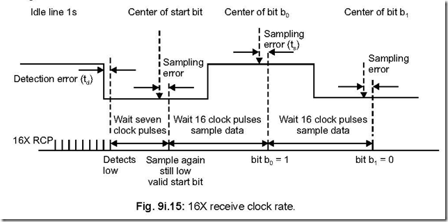
Ans. The situation is explained in Figure 9i.15 by clocking the UART receiver with 16X.
The difference in time between the beginning of a start bit and its detection is called detection error and is shown by td in the figure. The maximum time of detection is one RCP.
The difference in time between when a sample is taken (i.e., put into the receive shift register) and the actual centre of a data bit is called the sampling error and is shown by ts in Fig. 9i.15.
33. What happens to the maximum detection error when receive clock rate equals the receive data rate?
Ans. The maximum detection error would approach one bit time. Thus a start bit would not be detected until the very end of the start bit.
34. What is meant by clock slippage?
Ans. Clock slippage, also known by the name of clock skew, is a problem faced in asynchronous communication system.
In this case, the magnitude of sampling error increases with each successive sample in the data bit pattern. Thus, the clock may slip over or slip under the data.
Sometimes it may so happen that a data bit (it would start occurring for latter data bits in the data stream) may be sampled twice or not sampled at all in the clock period— it depends on whether the receive clock is higher or lower the transmit clock.
35. How the sampling error is related to sampling rate?
Ans. As the sampling rate is continued to be increased, the sampling error goes on decreasing.
As the sampling rate is increased, the sample time moves closer and closer to the centre of data bit, thereby decreasing the sampling error.

