8355/8755: Programmable I/O Ports with ROM/EPROM
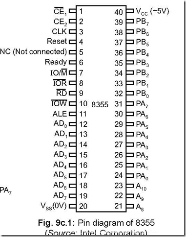
1. Draw the pin connection diagram of 8355.
Ans. The pin connection diagram of 8355 is shown in Fig. 9c.1.
2. Draw the functional block diagram of 8355 and discuss.
Ans. The functional block diagram of 8355 is shown in Fig. 9c.2.
3. What is the difference between 8355 and 8755?
Ans. The 2 KB memory for 8355 is a ROM, while that for 8755, it is EPROM.
Again for 8355, there are two chip enable signals—CE1 and CE 2, while for 8755 this
signal is designated as CE2.
Both have two I/O Ports—each I/O line of either port can be programmed either as
input or output.
4. What the DDR’s do?
Ans. There are two internal control registers, called Data Direction Registers (DDRs)—both the registers are 1-byte in length and designated as DDRA an DDRB. Each bit in the two DDR registers control the corresponding bit in the I/O ports. For example bit D0 of DDRA controls D0 bit of Port A and bit D5 of DDRB controls D5 bit of Port B.
5. How the two ports and the two DDRs are selected?
Ans. The bits AD1 and AD0 controls/selects one out of the four of the above. This is like this:
The IO/M signal is to remain high during the above.
6. How the 2 KB ROM of 8355 is accessed?
Ans. The 2 KB ROM of 8355 is accessed by the A10 – A0 latched address in conjunction with a low on IO/ M signal.


