The 8085 Microprocessor
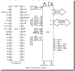
1. Draw the pin configuration and functional pin diagram of μP 8085. Ans. The pin configuration and functional pin diagram of μP 8085 are shown below:
2. In how many groups can the signals of 8085 be classified?
Ans. The signals of 8085 can be classified into seven groups according to their functions. These are:
(1) Power supply and frequency signals (2) Data and Address buses (3) Control bus
(4) Interrupt signals (5) Serial I/O signals (6) DMA signals (7) Reset signals.
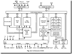
3. Draw the architecture of 8085 and mention its various functional blocks. Ans. The architecture of 8085 is shown below:
Fig. 2.2: Architecture of 8085
The various functional blocks of 8085 are as follows:
1.Registers
2.Arithmetic logic unit
3.Address buffer
4.Incrementer/decrementer address latch
5.Interrupt control
6. Serial I/O control
7.Timing and control circuitry
8.Instructions decoder and machine cycle encoder.
4. What is the technology used in the manufacture of 8085?
Ans. It is an NMOS device having around 6200 transistors contained in a 40 pin DIP package.
5. What is meant by the statement that 8085 is a 8-bit microprocessor?
Ans. A microprocessor which has n data lines is called an n-bit microprocessor i.e., the width of the data bus determines the size of the microprocessor. Hence, an 8-bit microprocessor like 8085 can handle 8-bits of data at a time.
6. What is the operating frequency of 8085?
Ans. 8085 operates at a frequency of 3 MHz, and the minimum frequency of operation is 500 kHz.
The version 8085 A-2 operates at a maximum frequency of 5 MHz.
7. Draw the block diagram of the built-in clock generator of 8085.
Ans. The built-in clock generator of 8085, in block schematic, is shown below:
The internal built-in clock generator, LC or RC tuned circuits, piezo-electric crystal or external clock source acts as an input to generate the clock. The T F/F, shown in Fig.
2.3 divides the input frequency by 2. Thus the output frequency of 8085 (obtained from pin 37) is half the input frequency.
8. What is the purpose of CLK signal of 8085?
Ans. The CLK (out) signal obtained from pin 37 of 8085 is used for synchronizing external devices.
9. Draw the different clock circuits which can be connected to pins 1 and 2 of 8085.
Ans. The different external clock circuits which can be connected to pins 1 and 2 of 8085 are shown below in Fig. 2.4:
Fig. 2.4: The different external clock circuits
The output frequency obtained from pin 37 of Fig. 2.4(b) is more stable than the RC circuit of Fig. 2.4(a).
10. What are the widths of data bus (DB) and address bus (AB) of 8085?
Ans. The width of DB and AB of 8085 are 8-bits (1 byte) and 16-bits (2 bytes) respectively.
11. What is the distinguishing feature of DB and AB?
Ans. While the data bus is bidirectional in nature, the address bus is unidirectional.
Since the mP can input or output data from within it, hence DB is bidirectional. Again the microprocessor addresses/communicates with peripheral ICs through the address bus, hence it is unidirectional, the address comes out via the AB of mP.
12. The address capability of 8085 is 64 KB. Explain.
Ans. Microprocessor 8085 communicates via its address bus of 2-bytes width – the lower byte AD0 – AD7 (pins 12-19) and upper byte D8 – D15 (pins 21–28). Thus it can address a maximum of 216 different address locations. Again each address (memory location) can hold 1 byte of data/instruction. Hence the maximum address capability of 8085 is
= 216 × 1 Byte
= 65, 536 × 1 Byte
= 64 KB (where 1 K = 1024 bytes)
13. Does 8085 have serial I/O control?
Ans. 8085 has serial I/O control via its SOD and SID pins (pins 4 and 5) which allows it to communicate serially with external devices.
14. How many instructions 8085 can support? Ans. 8085 supports 74 different instructions.
15. Mention the addressing modes of 8085.
Ans. 8085 has the following addressing modes: Immediate, Register, Direct, Indirect and Implied.
16. What jobs ALU of 8085 can perform?
Ans. The Arithmetic Logic Unit (ALU) of 8085 can perform the following jobs:
1.8-bit binary addition with or without carry.
2.16-bit binary addition.
3. 2-digit BCD addition.
4. 8-bit binary subtraction with or without borrow.
5. 8-bit logical OR, AND, EXOR, complement (NOT function).
6.bit shift operation.
17. How many hardware interrupts 8085 supports?
Ans. It supports five (5) hardware interrupts—TRAP, RST 7.5, RST 6.5, RST 5.5 and INTR.
18. How many I/O ports can 8085 access?
Ans. It provides 8-bit I/O addresses. Thus it can access 28 = 256 I/O ports.
19. Why the lower byte address bus (A0 – A7) and data bus (D0 – D7) are multiplexed? Ans. This is done to reduce the number of pins of 8085, which otherwise would have been a
48 pin chip. But because of multiplexing, external hardware is required to demultiplex
the lower byte address cum data bus.
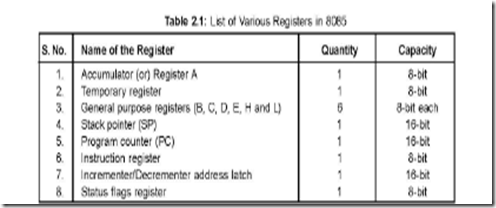
20. List the various registers of 8085.
Ans. The various registers of 8085, their respective quantities and capacities are tabulated below:
21. Describe the accumulator register of 8085.
Ans. This 8-bit register is the most important one amongst all the registers of 8085. Any data input/output to/from the microprocessor takes place via the accumulator (register). It is generally used for temporary storage of data and for the placement of final result of arithmetic/logical operations.
Accumulator (ACC or A) register is extensively used for arithmetic, logical, store and rotate operations.
22. What are the temporary registers of 8085?
Ans. The temporary registers of 8085 are temporary data register and W and Z registers. These registers are not available to the programmer, but 8085 uses them internally to hold temporary data during execution of some instructions.
23. Describe W and Z registers of 8085.
Ans. W and Z are two 8-bit temporary registers, used to hold 8-bit data/address during execution of some instructions.
CALL-RET instructions are used in subroutine operations. On getting a CALL in the main program, the current program counter content is pushed into the stack and loads the PC with the first memory location of the subroutine. The address of the first memory location of the subroutine is temporarily stored in W and Z registers.
Again, XCHG instruction exchanges the contents H and L with D and E respectively. W and Z registers are used for temporary storage of such data.
24. Describe the temporary data register of 8085.
Ans. The temporary data register of 8085 is an 8-bit register, which is not available to the programmer, but is used internally for execution of most of the arithmetic and logical operations.
ADD D instruction adds the contents of accumulator with the content of D. The content of D is temporarily brought into the temporary data register. Thus the two inputs to the ALU are—one from the accumulator and the other from the temporary data register. The result is stored in the accumulator.
25. Describe the general purpose registers of 8085?
Ans. The general purpose registers of 8085 are: B, C, D, E, H and L. They are all 8-bit registers but can also be used as 16-bit register pairs—BC, DE and HL. These registers are also known as scratch pad registers.
26. In what other way HL pair can be used?
Ans. HL register pair can be used as a data pointer or memory pointer.
27. Mention the utility of the general purpose registers.
Ans. General purpose registers store temporary data during program execution, which can also be stored in different accessible memory locations. But storing temporary data in memory requires bus access—hence more time is needed to store. Thus it is always advisable to store data in general purpose registers.
The more the number of general purpose registers, the more is flexibility in programming—so a microprocessor having more such registers is always advantageous.
28. Which are the sixteen bit registers of 8085.
Ans. 8085 has three (3) sixteen bit registers—Program Counter (PC), Stack Pointer (SP) and Incrementer/Decrementer address latch register.
29. Discuss the two registers program counter and stack pointer.
Ans. Program counter (PC) is a sixteen bit register which contains the address of the instruction to be executed just next. PC acts as a address pointer (also known as memory pointer) to the next instruction. As the processor executes instructions one after another, the PC is incremented—the number by which
the PC increments depends on the nature of the instruction. For example, for a 1-byte instruction, PC is incremented by one, while for a 3-byte instruction, the processor increments PC by three address locations.
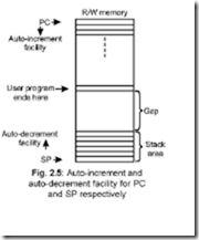
Stack pointer (SP) is a sixteen bit register which points to the ‘stack’. The stack is an area in the R/W memory where temporary data or return addresses (in cases of subroutine CALL) are stored. Stack is a auto- decrement facility provided in the system. The stack top is initialised by the SP by using the instruction LXI SP, memory address.
In the memory map, the program should Fig. 2.5: Auto-increment and be written at one end and stack should be auto-decrement facility for PC initialised at the other end of the map—this is and SP respectively done to avoid crashing of program. If sufficient
gap is not maintained between program memory location and stack, then when the stack gets filled up by PUSH or subroutine calls, the stack top may run into the memory area where program has been written. This is shown in Fig. 2.5.
30. Describe the instruction register of 8085.
Ans. Program written by the programmer resides in the R/W memory. When an instruction is being executed by the system, the opcode of the instruction is fetched from the memory and stored in the instruction register. The opcode is loaded into the instruction register during opcode fetch cycle. It is then sent to the instruction decoder.
31. Describe the (status) flag register of 8085.
Ans. It is an 8-bit register in which five bit positions contain the status of five condition flags which are Zero (Z), Sign (S), Carry (CY), Parity (P) and Auxiliary carry (AC). Each of these five flags is a 1 bit F/F. The flag register format is shown in Fig. 2.6:
* Sign (S) flag: – If the MSB of the result of an operation is 1, this flag is set, otherwise it is reset.
* Zero (Z) flag:– If the result of an instruction is zero, this flag is set, otherwise reset.
* Auxiliary Carry (AC ) flag:– If there is a carry out of bit 3 and into bit 4 resulting from the execution of an arithmetic operation, it is set otherwise reset.
This flag is used for BCD operation and is not available to the programmer to change the sequence of an instruction.
* Carry (CY) flag:– If an instruction results in a carry (for addition operation) or borrow (for subtraction or comparison) out of bit D7, then this flag is set, otherwise reset.
* Parity (P) flag:– This flag is set when the result of an operation contains an even number of 1’s and is reset otherwise.
32. State the characteristics of the flag register. Ans. The following are the characteristics of flag register:
z It is an 8-bit register.
z It contains five flags—each of one bit.
z The flag register can’t be written into.
33. What is the purpose of incrementer/decrementer address latch register?
Ans. This 16-bit register increments/decrements the contents of PC or SP when instructions related to them are executed.
34. Mention the blocks on which ALU operates?
Ans. The ALU functions as a part which includes arithmetic logic group of circuits. This includes accumulator, flags F/Fs and temporary register blocks.
35. What is the function of the internal data bus?
Ans. The width of the internal data bus is 8-bit and carries instructions/data between the CPU registers. This is totally separate from the external data bus which is connected to memory chips, I/O, etc.
The internal and external data bus are connected together by a logic called a bidirectional bus (transreceiver).
36. Describe in brief the timing and control circuitry of 8085.
Ans. The T&C section is a part of CPU and generates timing and control signals for execution of instructions. This section includes Clock signals, Control signals, Status signals, DMA signals as also the Reset section. This section controls fetching and decoding operations. It also generates appropriate control signals for instruction execution as also the signals required to interface external devices.
37. Mention the following:
(a) Control and Status signals
(b) Interrupt signals
(c) Serial I/O signals
(d) DMA signals
(e) Reset signals.
Ans. The control and status signals are ALE, RD , WR , IO/M , S0, S1 and READY.
The interrupt signals are TRAP, RST 7.5, RST 6.5, RST 5.5, INTR. INTA is an
interrupt acknowledgement signal indicating that the processor has acknowledged an
INTR interrupt.
Serial I/O signals are SID and SOD
DMA signals are HOLD and HLDA
Reset signals are RESET IN and RESET OUT.
38. What is the function of ALE and how does it function?
Ans. Pin 30 of 8085 is the ALE pin which stands for ‘Address Latch Enable’. ALE signal is used to demultiplex the lower order address bus (AD0 – AD7).
Pins 12 to 19 of 8085 are AD0 – AD7 which is the multiplexed address-data bus. Multiplexing is done to reduce the number of pins of 8085.
Lower byte of address (A0 – A7) are available from AD0 – AD7 (pins 12 to 19) during T1 of machine cycle. But the lower byte of address (A0 – A7), along with the upper byte A8 – A15 (pins 21 to 28) must be available during T2 and rest of the machine cycle to access memory location or I/O ports.
Now ALE signal goes high at the beginning of T1 of each machine cycle and goes low at the end of T1 and remains low during the rest of the machine cycle. This high to low transition of ALE signal at the end of T1 is used to latch the lower order address byte (A0 – A7) by the latch IC 74LS373, so that the lower byte A0 – A7 is continued to be available till the end of the machine cycle. The situation is explained in the following figure:
Fig. 2.7: Lower byte of address latching achieved by the H to L transition of ALE signal, which occurs at the end of T1 of each machine cycle
39. Explain the function of the two DMA signals HOLD and HLDA.
Ans. DMA mode of data transfer is fastest and pins 39 and 38 (HOLD and HLDA) become active only in this mode.
When DMA is required, the DMA controller IC (8257) sends a 1 to pin 39 of 8085. At the end of the current instruction cycle of the microprocessor it issues a 1 to pin 38 of the controller. After this the bus control is totally taken over by the controller.
When 8085 is active and 8257 is idle, then the former is MASTER and the latter is SLAVE, while the roles of 8085 and 8257 are reversed when 8085 is idle and 8257 becomes active.
40. ![]() Discuss the three signals IO/ M , S0 and S1.
Discuss the three signals IO/ M , S0 and S1.
![]() Ans. IO/ M signal indicates whether I/O or memory operation is being carried out. A high on this signal indicates I/O operation while a low indicates memory operation. S0 and S1 indicate the type of machine cycle in progress.
Ans. IO/ M signal indicates whether I/O or memory operation is being carried out. A high on this signal indicates I/O operation while a low indicates memory operation. S0 and S1 indicate the type of machine cycle in progress.
41. What happens when RESET IN signal goes low?
Ans. RESET IN is an input signal which is active when its status is low. When this pin is
low, the following occurs:
z The program counter is set to zero (0000H).
z Interrupt enable and HLDA F/Fs are resetted.
z All the buses are tri-stated.
z Internal registers of 8085 are affected in a random manner.
42. Is there any minimum time required for the effective RESET IN signal?
Ans. For proper resetting to take place, the reset signal RESET IN must be held low for at
least 3 clock cycles.
43. Indicate the function of RESET OUT signal.
Ans. When this signal is high, the processor is being reset. This signal is synchronised to the processor clock and is used to reset other devices which need resetting.
44. Write the advantages/disadvantages of having more number of general purpose registers in a microprocessor.
Ans. Writing of a program becomes more convenient and flexible by having more number of general purpose registers.
But there are certain disadvantages of having more GPRs. These are as follows:
The more the number of GPRs in a microprocessor, more number of bits would be required to identify individual registers. This would reduce the number of operations that can be provided by the microprocessor.
In programs involving subroutine CALL, if more GPRs are involved, then their
status are to be saved in stack and on return from the subroutine, they are to be restored
from the stack. This will thus put considerable overhead on the microprocessor.
If more number of GPRs are used in a microprocessor, considerable area of the chip
is used up in accommodating the GPRs. Thus there may be some problem in
implementing other functions on the chip.
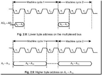
45. Draw the lower and higher order address bus during the machine cycles.
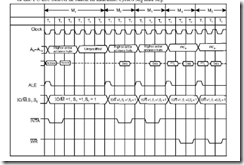
Ans. The lower byte of address (AD0 – AD7) is available on the multiplexed address/data bus during T1 state of each machine cycle, except during the bus idle machine cycle, shown in Fig. 2.8.
The higher byte of address (A8 – A15) is available during T1 to T3 states of each machine cycle, except during the bus idle machine cycle, shown in Fig. 2.9.
46. Draw the appearance of data in the read and write machine cycles.
Ans. Data transfer from memory or I/O device to microprocessor or the reverse takes place during T2 and T3 states of the machine cycles.
In the read machine cycle, data appears at the beginning of T3 state, whereas in the write machine cycle, it appears at the beginning of T2, shown in Fig. 2.10.
Fig. 2.10: Data bus
47. Draw the status signals during opcode fetch and memory read machine cycles.
![]() Ans. The status signals are IO/ M , S0 and S1. Their conditions indicate the type of machine cycle that the system is currently passing through. These three status signals remain active right from the beginning till the end of each machine cycle, shown in Fig. 2.11.
Ans. The status signals are IO/ M , S0 and S1. Their conditions indicate the type of machine cycle that the system is currently passing through. These three status signals remain active right from the beginning till the end of each machine cycle, shown in Fig. 2.11.
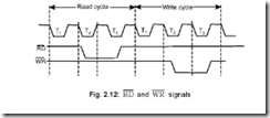
48. Show the RD and WR signals during the Read cycle and Write cycle.
Ans. When RD is active, microprocessor reads data from either memory or I/O device while
when WR is active, it writes data into either memory or I/O device.
Data transfer (reading/writing) takes place during T2 and T3 states of read cycle or write cycle and is shown in Fig. 2.12.
49. Indicate the different machine cycles of 8085.
Ans. 8085 has seven different machine cycles. These are:
(1) Opcode Fetch (2) Memory Read (3) Memory Write (4) I/O Read (5) I/O Write
(6) Interrupt Acknowledge (7) Bus Idle.
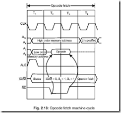
50. Draw the Opcode Fetch machine cycle of 8085 and discuss.
Ans. The first machine cycle of every instruction is the Opcode Fetch. This indicates the kind of instruction to be executed by the system. The length of this machine cycle varies between 4T to 6T states—it depends on the type of instruction. In this, the processor places the contents of the PC on the address lines, identifies the nature of machine cycle
(by IO/M , S0, S1) and activates the ALE signal. All these occur in T1 state.’’
In T2 state, RD signal is activated so that the identified memory location is read from
and places the content on the data bus (D0 – D7).
In T3, data on the data bus is put into the instruction register (IR) and also raises
the RD signal thereby disabling the memory.
In T4, the processor takes the decision, on the basis of decoding the IR, whether to enter into T5 and T6 or to enter T1 of the next machine cycle.
One byte instructions that operate on eight bit data are executed in T4. Examples are ADD B, MOV C, B, RRC, DCR C, etc.
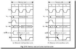
51. Briefly describe Memory Read and Write machine cycles and show the wave- forms.
Fig. 2.14: Memory read and write machine cycle
Ans. Both the Memory Read and Memory Write machine cycles are 3T states in length. In Memory Read the contents of R/W memory (including stack also) or ROM are read while in Memory Write, it stores data into data memory (including stack memory).
As is evident from Fig. 2.14 during T2 and T3 states data from either memory or CPU are made available in Memory Read or Memory Write machine cycles respectively. The
![]() status signal (IO/ M , S0, S1) states are complementary in nature in Memory Read and Memory Write cycles. Reading or writing operations are performed in T2.
status signal (IO/ M , S0, S1) states are complementary in nature in Memory Read and Memory Write cycles. Reading or writing operations are performed in T2.
In T3 of Memory Read, data from data bus are placed into the specified register (A,
B, C, etc.) and raises RD so that memory is disabled while in T3 of Memory Write
WR signal is raised which disables the memory.
52. Draw the I/O Read and I/O Write machine cycles and discuss.
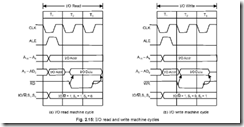
![]() Ans. I/O Read and Write machine cycles are almost similar to Memory Read and Write machine cycles respectively. The difference here is in the IO/ M signal status which remains 1 indicating that these machine cycles are related to I/O operations. These machine cycles take 3T states.
Ans. I/O Read and Write machine cycles are almost similar to Memory Read and Write machine cycles respectively. The difference here is in the IO/ M signal status which remains 1 indicating that these machine cycles are related to I/O operations. These machine cycles take 3T states.
In I/O read, data are available in T2 and T3 states, while during the same time (T2 and T3) data from CPU are made available in I/O write.
The I/O read and write machine cycles are shown in Fig. 2.15.
Fig. 2.15: I/O read and write machine cycles
53. Draw the Interrupt Acknowledge cycles for (a) RST instruction (b) CALL instruction.
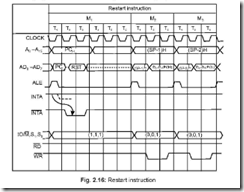
In M1, RST is decoded. This initiates a CALL to the specific vector location. Contents of the PC are stored in stack in machine cycles M2 and M3.
Fig. 2.17: Timing diagram of INTA machine cycle and execution of call instruction
The above figure shows an Interrupt Acknowledge cycle for CALL instruction. M2 and M3 machine cycles are required to call the 2 bytes of the address following the CALL. Memory write are done in machine cycles M4 and M5 in which contents of PC are stored in stack and then a new instruction cycle begins.
54. What is meant by Bus Idle Machine cycle?
Ans. There are a few situations in which machine cycles are neither Read or Written into.
These are called Bus Idle Machine cycle.
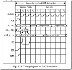
Such situations arise when the system executes a DAD or during the internal opcode generation for the RST or TRAP interrupts.
The ALE signal changes state during T1 of each machine cycle, but in Bus Idle Machine cycles, ALE does not change state.
55. Explain the DAD instruction and draw its timing diagram.
Ans. DAD instruction adds the contents of a specified register pair to the contents of H and L. For execution of DAD, 10 T-states are needed. Instead of having a single machine cycle having 10 T-states, it consists of the Opcode Fetch machine cycle (4T states) and 6
extra T-states divided into two machine cycles. These two extra machine cycles are Bus
Idle Machine cycles which do not involve either memory or I/O.
56. Discuss the concept of WAIT states in microprocessors.
Ans. So many times it may happen that there is speed incompatibility between microprocessor and its memory and I/O systems. Mostly the microprocessor is having higher speed.
So in a given situation, if the microprocessor is ready to accept data from a peripheral device while there is no valid data in the device (e.g. an ADC), then the system enters into WAIT states and the READY pin (an input pin to the microprocessor, pin no. 35 for 8085) is put to a low state by the device.
Once the device becomes ready with some valid data, it withdraws the low state on the READY pin of 8085. Then 8085 accepts the data from the peripheral by software instructions.
57. Does 8085 have multiplication and division instructions?
Ans. No, 8085 does not have the above two instructions. It can neither multiply nor divide two 8-bit numbers. The same are executed by the processor following the process of repetitive addition or subtraction respectively.
58. Indicate the bus drive capability of 8085.
Ans. 8085 buses can source up to 400 mA and sink 2 mA of current. Hence 8085 buses can drive a maximum of one TTL load.
Thus the buses need bus drivers/buffers to enhance the driving capability of the buses to ensure that the voltage levels are maintained at appropriate levels and malfunctioning is avoided.
59. What are the buffers needed with the buses of 8085?
Ans. An 8-bit unidirectional buffer 74LS244 is used to buffer the higher order address bus (A8 – A15). It consists of eight non-inverting buffers with tri-state outputs. Each pin can sink 24 mA and source 15 mA of current.
A bidirectional buffer 74LS245 (also called octal bus transreceivers) can be used to drive the bidirectional data bus (D0 – D7) after its demultiplexing. The DIR pin of the IC controls the direction of flow of data through it.
60. Explain the instruction cycle of a microprocessor.
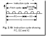
Ans. When a processor executes a program, the instructions (1 or 2 or 3 bytes in length) are executed sequentially by the system. The time taken by the processor to complete one instruction is called the Instruction Cycle (IC).
An IC consists of Fetch Cycle (FC) and an Execute Cycle (EC). Thus IC = FC + EC. It is shown in Fig. 2.19. Depending on the type of instruction, IC time varies.
61. Explain a typical fetch cycle (FC).
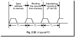
Ans. The time required to fetch an opcode from a memory location is called Fetch Cycle.
A typical FC may consist of 3T states. In the first T-state, the memory address, residing in the PC, is sent to the memory. The content of the addressed memory (i.e., the opcode residing in that memory location) is read in the second T-state, while in the third T-state this opcode is sent via the data bus to the instruction register (IR). For slow memories, it may take more time in which case the processor goes into ‘wait cycles’. Most microprocessors have provision of wait cycles to cope with slow memories.
A typical FC may look like the following:
62. Draw the block schematic of a typical Instruction Word flow diagram and explain the same.
Ans. There are two kinds of words—instruction word and data word. The 2 byte content of the PC is transferred to a special register–called memory address register (MAR) or simply address register (AR) at the beginning of the fetch cycle. Since the content of MAR is an address, it is thus sent to memory via the address bus. The content of the addressed memory is then read under ‘Read control’ generated by T&C section of the microprocessor. This is then sent via the data bus to the memory data register (MDR) or simply data register (DR) existing in CPU. This is placed in the instruction register (IR) and is decoded by the instruction decoder and subsequently executed. The PC is then incremented if the subsequent memory location is to be accessed.
63. Draw the block schematic of a typical data word flow diagram and explain the same.
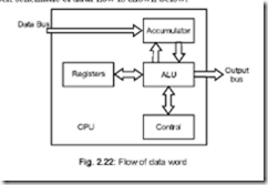
Ans. The data word flows via the data bus into the accumulator. The data source can be a memory device or an input device. Data from the accumulator is then manipulated in ALU under control of T & C unit. The manipulated data is then put back in the accumulator and can be sent to memory or output devices.
The block schematic of data flow is shown below.
64. Why a microprocessor based system is called a sequential machine?
Ans. It can perform the jobs in a sequential manner, one after the other. That is why it is called a sequential machine.
65. Why a microprocessor based system is called a synchronous one?
Ans. All activities pertaining to the µP takes place in synchronism with the clock. Hence it is called a synchronous device.
66. Draw the diagram which will show the three buses separately, with the help of peripheral ICs.
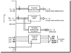
Ans. The scheme of connections is shown below. The octal bus driver 74LS244 drives the higher order address bus A15 – A8 while 74LS373 Latch drives the lower order address bus A7 – A0 (with the help of ALE signal). The bidirectional bus driver 74LS245 drives the
data bus D7 – D0 while the 74LS138 (a 3 to 8 decoder chip) outputs at its output pins IOW, IOR, MEMW, MEMR, signals from the IO/ M , RD and WR signals of 8085.
Fig. 2.23: Demultiplexing of address/data bus and separation of control signals
67. Discuss the status of WR and RD signals of 8085 at any given instant of time.
Ans. At any given instant, the status of the two signals WR and RD will be complementary
to each other.
It is known that microprocessor based system is a sequential device, so that at any given point of time, it does the job of reading or writing—and definitely not the two jobs
at the same time. Hence if WR signal is low, then RD signal must be high or vice versa.
68. Which registers of 8085 are programmable?
Ans. The registers B, C, D, E, H and L are programmable registers in that their contents can be changed by programming.
69. Suggest the type of operations possible on data from a look of the architecture of 8085.
Ans. The architecture of 8085 suggests that the following operations are possible.
z Uses the temporary registers during arithmetic operations.
z Checks for the condition of resultant data (like carry, etc.) from the flag register.
70. What are the externally initiated operations supported by 8085?
Ans. 8085 supports several externally initiated operations at some of its pins. The operations possible are:
z Resetting (via Reset pin)
z Interruptions (via Trap, RST 7.5, RST 6.5, RST 5.5 and Interrupt pin)
z Ready (via Ready pin)
z Hold (via Hold pin)
71. Name the registers not accessible to the programmer. Ans. The following registers cannot be accessed by the programmer:
z Instruction register (IR)
z Memory address register (MAR) or supply address register (AR)
z Temporary registers.
72. Name the special purpose registers of 8085.
Ans. The special purpose registers used in 8085 microprocessor are:
z Accumulator register (A)
z Program counter register (PC)
z Status (or Flag) register
z Stack pointer register (SP)
73. What should be the size of the Instruction Register if an arbitrary microprocessor has only 25 instructions?
Ans. The length of the Instruction Register would be 5-bits, since 25 = 32, since a 5-bit Instruction Register can decode a maximum of 32 instructions.
74. Explain the difference between HLT and HOLD states.
Ans. HLT is a software instruction. Its execution stops the processor which enters into a HALT state and the buses of the processor are driven into tri-state.
HOLD is an hardware input to the processor. When HOLD input = 1, the processor goes into the HOLD state, but the buses don’t go into tri-state. The processor gives out a high HLDA (hold acknowledge) signal which can be utilised by an external device (like a DMA controller) to take control of the processor buses. HOLD is acknowledged by the processor at the end of the current instruction execution.
75. Indicate the length of the Program Counter (PC) to access 1 KB and 1 MB memory.
Ans. 1 KB = 1024 bytes
and 1 MB = 1024 K bytes
Thus the required number of bits in PC to access 1 KB are 10 (210 = 1024) and 20 (220 = 1024 K) respectively.
76. What determines the number of bytes to be fetched from memory to execute an instruction?
Ans. An instruction normally consists of two fields. These are:
Thus, while the system starts executing an instruction, it first decodes the opcode which then decides how many more bytes are to be brought from the memory—its minimum value is zero (like RAR) while the maximum value is two (like STA 4059 H).
77. A Microprocessor’s control logic is ‘microprogrammed’. Explain.
Ans. It implies that the architecture of the control logic is much alike the architecture of a
very special purpose microprocessor.
78. Does the ALU have any storage facility?
Ans. No, it does not have any storage facility. For this reason, the need for temporary data
registers arise in ALU–it has two inputs: one provided by the accumulator and the other
from the temporary data register. The result of summation is stored in the accumulator.
