5.5 MEMORY-MAPPED I/O
In, memory-mapped I/O, the input and output devices are assigned and identified by 16-bit addresses. To transfer data between the microprocessor and I/O devices, memory- related instructions (such as LD A, (16-bit) and memory control signals (such as M̅R̅E̅Q̅) are used. The microprocessor communicates with an I/O device as if it were one of the memory locations.
5.5.1 Memory-Related Data Transfer Instructions
To understand the memory-mapped I/O technique, we need to examine how a data byte is transferred from the Z80 to a memory location or vice versa. For example, the following instruction will transfer (copy) the contents of the accumulator to the memory location 8000H• It is assumed here that the instruction is stored in memory locations 2050H, 51H, and 52H•
This is a 3-byte instruction; the first byte is the opcode, and the second and the third bytes specify the memory address. However, the 16-bit address 8000H is entered in the reverse order; the low-order byte 00 is stored in location 2051, followed by the high-order address 80H (the reason for the reversed order will be explained in section 5.9).In this example, if an output device instead of a memory register is connected at this address, the accumulator contents will be transferred to the output device. This is called the memory-mapped I/O technique.
Similarly, the instruction LD A, (4000H) will transfer the contents of the memory location 4000H to the accumulator. To assign this address for a memory mapped input port, we can interface an input device (for example a keyboard) instead of memory by using the memory-related control signals (MREQ and RD). When the processor executes the instruction, the accumulator receives data from the input device rather than from a memory register 4000H•
5.5.2 Execution of Memory-Related Data Transfer Instructions
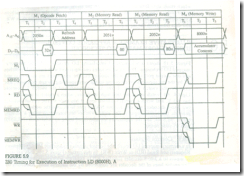
The execution of memory-related instructions discussed in the previous section is similar to the execution of I/O instructions (Sections 5.1 and 5.3), except that the memory-related instructions have 16-bit addresses. Figure 5.9 shows the execution of the instruction LD (8000H), A. It has four
machine cycles; in the first three machine cycles, the Z80 reads the three bytes. The fourth machine cycle M4 (Memory Write) is similar to the machine cycle M3 of the OUT instruction. In this machine cycle, the Z80 places the 16-bit address 8000H on the address bus and the accumulator contents on the data bus. This is followed by the assertion of the control signals M̅R̅E̅Q̅ and W̅R̅ .The information available during M4 can be used to interface a memory-mapped output port with the 16-bit address 8000H•
In memory-mapped I/O, I/O selection and data transfer require steps similar to those required in peripheral-mapped I/O:
1. Decode the entire address bus A15-A0 (rather than just A7-A0 )
2. Combine the control signals M̅R̅E̅Q̅, W̅R̅, and the decoded pulse from Step 1 to generate a pulse similar to the M̅S̅E̅L̅ pulse, which will be used to select an I/O rather than memory.
3. Use the I/O select pulse (actually M̅S̅E̅L̅) to enable the I/O port.
To interface a memory-mapped input port, the steps are similar to those of the memory-mapped output port. We can use the instruction LD A, (16-bit), which reads data from an input port with the 16-bit address and places it in the accumulator. The instruction has four machine cycles; only the fourth machine cycle differs from M4 in Figure 5.9. The control signal will be R̅D̅ rather than W̅R̅, and data flow from the input port to the microprocessor.

