5.3 INTERFACING INPUT DEVICES
The interfacing of input devices is almost identical to that of interfacing output devices, but with some differences in bus signals and circuit components. In this discussion, we will assume that you are familiar with the basic concepts of interfacing (Section 5.1.3) and describe only the additional details. First, we examine the execution and timing of the IN instruction and discuss the interfacing of input devices in relation to the timing diagram.
5.3.1 IN Instruction
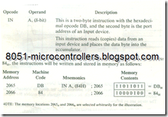
The Z80 instruction set includes several instructions to read (copy) data from such. Input devices as switches, keyboards, and A/D data converters. These instructions can read an input device and place the data into the accumulator, Z80 registers, or memory registers. These are two-byte instructions; the first byte is the opcode, and the second byte specifies the port address. Although there are numerous ways of specifying the port address, it is always eight bits long. Thus, the addresses for input devices can range from 00H to FFH• among the several Input instructions available, the machine cycles and timing of the following instruction will be examined.
When the microprocessor is asked to execute these instructions, it will first read the machine codes (or bytes) stored at locations 2065H and 2066H, then read the switch positions at port 84H by enabling the interfacing device of the port. The data byte indicating switch positions from the input port will be placed in the accumulator. To design an interfacing circuit with the port address 84H• we now need to examine the machine cycles and execution timing of the IN instruction.
5.3.2 Execution of IN Instruction and Its Timing:
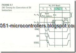
The IN instruction has three machine cycles: Opcode Fetch, Memory Read, and I/O Read. In the first two machine cycles, the Z80 reads the opcode DB and the port address 84H (see example in previous section). These cycles are identical to the first two machine cycles of the OUT instruction shown in Figure 5.1. In the third machine cycle, the Z80 reads a data byte from the input port as follows (Figure 5.7):
1. The port address 84H is placed on the low-order address bus at the beginning of the machine cycle M3 (I/O Read).
2. During T2, the control signals I͞͞O͞R͞Q͞ and R̅D̅ are asserted, and one Wait state is inserted automatically after T2•
3. During T3, the Z80 reads the data bus and then causes the control signals (I͞͞O͞R͞Q͞ and R̅D̅) to go inactive.
5.3.3 Basic Concepts in Interfacing Input Devices
To interface an input port with the address 84H, we need to logically AND the information on the address bus with the control signals and enable the input port. The steps are as follows:
1. Decode the low-order bus to generate the I/O address pulse.
2. Combine the I/O address pulse with the control signals I͞͞O͞R͞Q͞ and R̅D̅ to generate the signal I/O Select (I̅O̅S̅E̅L̅, Figure5.8). Another approach is to combine I͞͞O͞R͞Q͞ and R̅D̅ to generate an I̅O̅R̅D̅ signal and then to combine the I̅O̅R̅D̅ with the I/O address pulse to generate the I/O select pulse.
3. Enable the input interfacing device using the I/O select pulse.
These steps are identical to those listed for interfacing output devices; the only differences are (1) the control signal is R̅D̅ instead of W̅R̅, and (2) data flow from an input port to the accumulator rather than from the accumulator to an output port.

