Interfacing I/O Devices
The I/O (Input/Output) is the third component of a microprocessor-based system. I/O devices, such as keyboards and displays, are the ears and eyes of the MPUs; they are the communication channels to the "outside world." Data can enter or exit in groups of eight bits using the entire data bus; this is called the parallel I/O mode. The other mode is the serial I/O, whereby one bit is transferred using one data line; typical examples include peripherals such as CRT terminals or cassette tapes. In this chapter, we focus on interfacing I/O devices in the parallel mode; the serial mode will be discussed in the topic.
In the parallel I/O mode, devices can be interfaced using two techniques: peripheral mapped I/O and memory-mapped I/O. In peripheral-mapped I/O, a device is identified with an 8-bit address and enabled by I/O-related control signals. In memory-mapped I/O, a device is identified with a 16-bit address and enabled by memory-related control signals. The process of data transfer in both is identical. Each device is assigned a binary address through its interfacing circuit. When the Z80 is programmed to transfer data, it places the appropriate address on the address bus,
Sends the control signals, enables the interfacing device, and transfers data. The interfacing device is like a gate for data bits, which is opened by the MPU whenever it intends to transfer data.
To grasp the essence of interfacing techniques, we first examine the machine cycles of I/O instructions to determine the timings for I/O data arriving on the data bus, and then latch (or catch) that information.
We derive the basic concepts of peripheral-mapped and memory mapped I/O from the machine cycles. The peripheral-mapped I/O concepts are illustrated with two examples: interfacing LEDs as an output device and switches as an input device. The memory-mapped I/O technique is illustrated with an example of appliance control. The chapter also includes additional interfacing examples that occur frequently in microprocessor based products.
OBJECTIVES:
· Illustrate the Z80 bus contents and control signals when OUT and IN instructions are executed.
· Explain the necessity of Wait states in I/O machine cycles.
· Recognize the device (port) address of a peripheral-mapped I/O by analyzing the associated logic circuit.
· Recognize the device (port) address of a memory-mapped I/O by analyzing the associated logic circuit.
· Explain the differences between the peripheral-mapped and memory-mapped I/O techniques.
· Interface an I/O device to the Z80 microprocessor for a specified device address by using logic gates and such MSI chips as decoders, latches; and buffers.
· Explain the concepts in interfacing analog devices such as sensors and motors.
INTERFACING OUTPUT DEVICES:
In peripheral-mapped I/O, a device is identified with an 8-bit address, and I/O related control signals are used to enable the device. The process of data transfer is in many ways similar to that of reading from or writing into a memory register. The Z80 uses the instruction IN to read (input) data from an input device and uses the instruction OUT to write (send) data to an output device. To understand interfacing of I/O devices, we need to examine the execution and machine cycles. Of these input/output instructions. In the next section, we will examine the execution of the OUT instruction and discuss the interfacing of output devices, and in Section 5.3, we will examine the IN instruction and discuss the interfacing of input devices.
5.1.1 OUT Instruction
The Z80 microprocessor has several output instructions to send (copy or write) data to an output device. It can send data from the accumulator, internal general purpose registers, or memory registers to an output device. The Out instructions include the 8-bit address of a device as an operand. Therefore, the address can be any of the 256 8-bit binary combinations from OOH to FFH• Thus, an output device can be assigned any 8-bit address between OOH and FFH through an appropriate interfacing circuit. The address range from OOH to FFH is called the I/O or peripheral map, and an address can be referred to as a device address, port address, or port number. Among the several Out instructions, we will examine the machine cycles and timing of the following instruction.
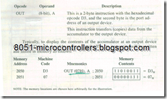
This is a 2-byte instruction with the hexadecimal opcode D3, and the second byte is the port address of an output device.
This instruction transfers (copies) data from the accumulator to the output device.
Typically, to display the contents of the accumulator at an output device (such as LEDs) with the address, for example, 07H, the instruction will be written and stored in memory as follows:
When the microprocessor reads and executes the machine codes written at memory registers 2050H and 2051H, it will transfer (copy) the byte from the accumulator to the LED port with address 07H and display the byte. Now the question remains: How is the address 07H assigned to the output port? To answer that question, we need to examine the machine cycles of this instruction, as shown in the next section.
5.1.2 Execution of OUT Instruction and Timing
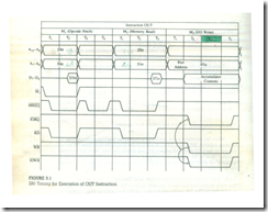
The OUT instruction has three machine cycles: Opcode Fetch, Memory Read, and I/O Write. The Z80 reads the opcode and the port address from memory in the first two machine cycles and writes into the port in the third cycle. Figure 5.1 shows the timing of the OUT instruction with the port address 07H•
The first two machine cycles-Opcode Fetch and Memory Read-are similar to the machine cycles shown in Figure 3.5; however, in Figure 5.1, the low order and high-order address buses are shown separately to illustrate the contents of the low-order bus in the third cycle. In the Opcode Fetch cycle, the Z80 places the address 2050H on the address bus and fetches the opcode D3H (1 1 0 I 00 1 1) via the data bus. When the Z80 decodes the opcode, it realizes that the instruction consists of two bytes, and that it must read the second byte. In the second machine cycle, the Z80 places the next address, 2051H, on the address bus and reads the port address 07H•
In the third machine ‘cycle, M3 (I/O Write), the following events occur:
1. The Z80 places the port address 07 H on the low-order address bus and the contents of the accumulator on the data bus.
2. During T2, it asserts the I͞͞O͞R͞Q͞ and ͞͞͞͞W͞͞R͞ control signals; the assertion of I͞͞O͞R͞Q͞ indicates that it is an I/O operation.
3. The Z80 automatically inserts a single Wait state Tw after T2 to allow sufficient response time for an I/O device; this Wait state is added regardless of the WAIT signal status.
4. During T3, the control signals I͞͞O͞R͞Q͞ and W͞͞R͞ become inactive.
To interface an output device, the information on the buses during the M3 cycle is critical. From the beginning of T2 until the end of T3, we have the port address (07H) on the low-order address bus and the data byte to be displayed on the data bus. The availability of this information is indicated by the control signals. Now what we must do is to latch (catch) this information using the control signals before it disappears from the buses; we need to open the gate at that precise moment to let the data flow to the "outside world." This is the essence of interfacing.

