5.2 ILLUSTRATIVE EXAMPLE 1: INTERFACING LEDS
In this section, we will analyze an actual interfacing circuit with the port address 07H to display binary data at an LED port and a single digit at a seven-segment LED. A group of 8 LEDs will be used to indicate binary I s and Os and will be’ connected to the data bus using the 7475 latches. Similarly, an interfacing of a seven-segment LED will be demonstrated using an octal latch 74LS373.
5.2.1 Hardware
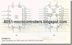
Figure 5.3 shows the logic symbols of the 7475 latch. It has four bistable latches controlled by the active high enable signals; E1_2 enables the first two latches and E3-4 enables the remaining two. When E is high, data enter the latch and appear at the Q outputs, and Q outputs correspond to the input data, When E goes from high to low, data will be latched and will remain stable until E goes high again.
. When Q output is high, it can supply (source) 400 µA, and when it is low, it can sink 16 mA current. Since most LEDs require a 10-15 mA current to be properly illuminated, they are connected to ͞Q output of the latch so that when the input is high, ͞Q output is low and the LED is turned on.
Figure 5.3(b) shows the logic symbol of an octal latch 74LS373. This is similar to the 7475 latch, except that the latch is followed by a tri-state buffer. The latch and the buffer are controlled independently by Latch Enable (LE) and Output Enable (O͞E͞). When LE goes high, the data enter the latch, and when LE goes low, data are latched. The latched data are available on the output lines of the 74LS373 if the buffer is enabled by O͞E͞ (active low). If O͞E͞ is high, the output lines go into high impedance state. The advantage of using the octal latch is that it has eight latches in a package (vs. four in 7475), and when the buffer is not enabled, it remains in high impedance state, thus minimizing the loading on the data bus. In addition, it has two control signals (LE and O͞E͞); this can be advantageous in some interfacing circuits.
5.2.2 Interfacing Circuit
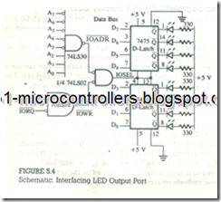
Figure 5.4 shows an interfacing circuit for the LED output port with the address 07 H. We will analyze this circuit in terms of the three steps for interfacing output devices as outlined in Section 5.1.3.
1. An 8-input NAND gate with five inverters is used to decode the low-order address bus A7-A0. The output of the NAND gate is asserted when the address is 0 0 0 0 0 1 1 1 (07H); thus, the NAND gate performs the decoding function to generate the I/O address (l͞O͞A͞D͞R͞) pulse.
2. The control signals I͞͞O͞R͞Q͞ and W͞͞R͞ are ANDed in a negative AND gate (physically, an OR gate) to generate the control signal IOW͞͞R͞ (active low). The IOW͞͞R͞ is again ANDed (through a NOR gate) with the I/O address pulse to
generate the I/O select pulse (active high).The IOSEL pulse is asserted only when the address is 07H and the control signals I͞͞O͞R͞Q͞ and W͞͞R͞ are low.
3. The IOSEL pulse is used to enable the latches 7475. The data bus D7-D0 is connected to the D input, and the LED cathodes are connected to the Q̅ output of the latch. The LED anodes are connected to the + 5 V power supply through the current-limiting resistors.
At the beginning of T2 in the third machine cycle shown in Figure 5.1, the control signals I͞O͞R͞Q͞ and ̅W̅͞͞R̅͞ are asserted, and the I/O select pulse (Figure 5.4) goes high If the address is 07H• When the I/O select pulse goes high, the data on the data bus enter the latches. During T3, when the control signals become inactive, the I/O select pulse goes low, and the data are latched. The logic is on the data lines turn on the corresponding LEDs because when a data bit is high, the Q̅ output is low and the LED is turned on.
INSTRUCTIONS
To display data, for example, 97H, at this LED port, instructions are as follows:
The first instruction (LD) stores the second byte 97H in the accumulator, and the OUT instruction sends the byte (97H) from the accumulator to the LED port 07H• When the l/O select pulse is asserted, the byte 97H enters the latch and is displayed by the LEDs. When LOSEL goes low (inactive), the byte is latched and continues to be displayed by the LEDs.
5.2.3 Using a Seven-Segment LED as a Display Device
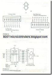
A seven-segment LED consists of seven light-emitting diodes (A through G) and one diode (DP) for the decimal point; these LEDs are physically arranged as shown in Figure 5.5(a). To display a number, the necessary segments are lit by sending an appropriate signal for current flow through diodes. For example, to display 8, all segments should be lit. To display I, segments Band C must be lit. Seven-segment LEOs are available in two types: common cathode and common anode. They can be represented schematically as in Figures 5.5(b) and (c). The segments, A through G, are usually connected to data lines D0 through 06, respectively. If the decimal point is being used, data line D7 is connected to DP; otherwise it can be left open. Current flow in these diodes must be limited to 20mA.
Figure 5.6 shows the interfacing of a common-anode seven-segment LED using the latch 74LS373. This circuit assumes the same decoding network as in Figure 5.4, thus assigning the port address 07H to the latch. The differences between Figures 5.4 and 5.6 are that the binary LEDs in Figure 5.4 are replaced by the seven-segment LED, and the latch 7475 is replaced by the octal latch 74LS373. The binary code required to display a digit is determined by the type of the seven segments LED (common cathode or common anode) and the connections of the
data lines. For example, in Figure 5.6, to display digit I at the output port, segments Band C should be turned on, and these segments are turned on with logic 0. Therefore, the binary code should be 79H as follows:
The code for each Hex digit from 0 to F can be determined by examining the connections of the data lines to the segments and the logic requirements.
When the microprocessor executes the OUT instruction, the IOSEL goes active and enables (LE) the latch, and the code 79H is passed on from the data bus to the latches. The output buffer of the latch is already enabled by grounding O͞E͞;thus, the code displays digit I at the seven-segment LED by turning on the segments B and C. The latch can sink 24 mA when the output logic is low; the current limiting resistors 330Ώ controls the current flow through the lighted segments. Now the question is, Why not use a common cathode LED? If a common-cathode seven segment LED is used in this circuit, the output of the latch would have to be high to drive the segments. The latch can supply approximately 2.6 mA when the output is high; this current is insufficient to drive the segments.


