After examining the concepts summarized at the end of the previous section, we may need to generate additional control signals.
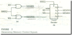
1. To read from memory, the M͞R͞E͞Q and the R͞D signals are necessary, and to read from an input device, the I͞O͞R͞Q and the R͞D are necessary; all these signals are active low. As a design practice, the M͞R͞E͞Q is generally combined with a decoded address (discussed in Topic4). and R͞D is connected directly to the memory chip. However, control signals R͞D and W͞R can also be combined with M͞R͞E͞Q and I͞O͞R͞Q to generate additional signals. We can generate active low Memory Read (M͞E͞M͞R͞D) signal either by ANDing these signals in a negative NAND gate as shown in Figure 7(a) or by using a 2-to-4 decoder as shown in Figure 7(b). The decoder is enabled by the M͞R͞E͞Q and has R͞D and W͞R signals as input. Both inputs cannot be active at the same time; when one is low, the other will remain high, When R͞D is active low, the input is 0 1 , and the output O1 goes active as M͞E͞M͞R͞D.
2. To write into memory, the M͞R͞E͞Q and the W͞R signals are necessary. and to write a data byte to an output device, the I͞O͞R͞Q and W͞R signals are necessary;
FIGURE 7
Generating Memory Control Signals
all these signals are active low. We can generate active low Memory Write (M͞E͞M͞W͞R) signal by ANDing M͞R͞E͞Q and W͞R signals in a negative NAND gate as shown in Figure 7(a) or by using the decoder as shown in Figure 7(b). Similarly, I͞O͞R͞D (I/O Read) and I͞O͞W͞R (I/O Write) signals can be generated; this is discussed in Topic5.
