1- The MOS Technology 6501 microprocessor chip has 13 address lines. Specify the memory registers it is capable of addressing.
2- If the Intel 8086 microprocessor has 20 address lines, what is its capacity of memory addressing?
3- Explain the functions of the accumulator.
4- List the Z80 programmable registers.
5- What is a flag?
6- What is the function of the program counter?
7- If the Z80 is executing the code fetched from the memory location 1845H, what is the memory address in the program counter?
8- If the clock frequency is 4 MHz, how much time is required to execute an instruction of 21 T-states?
9- The instruction LD IX, (2050H) loads 2050H into the index register. Specify the number of bytes. machine cycles, and T-states of this instruction by checking the instruction set. Calculate the time required to execute the instruction if the system clock frequency is 6 MHz.
10- List the sequence of events that occurs when the Z80 reads from memory.
11- In the Opcode Fetch cycle, what are the control signals required to enable the memory buffer?
12- When is the data byte placed on the data bus in the Memory Write cycle?
13- The memory location 2065H holds the opcode F9H , If the Z80 begins the Opcode Fetch cycle by placing the address 2065H on the address bus, specify the contents of the data bus after the falling edge of the T2 state.
14- The instruction LD B, (HL) copies the contents of the memory location specified by the 16-bit contents in the Hl, register. It is a l-byte instruction with two machine cycles. Identify the second machine cycle and its control signals.
15- In Figure 7(b), exchange R͞D and W͞R signals and identify the output pins and the control signals that can be generated at the output.
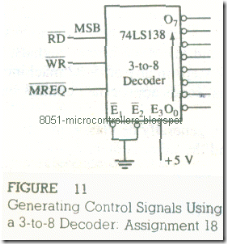
16- Figure 11 shows a 3-to-8 decoder with M͞R͞E͞Q. R͞D, and W͞R as input signals. Identify the control signals that can be generated at the outputs of the decoder.
FIGURE 11
Generating Control Signals Using a 3-to-8 Decoder: Assignment 18
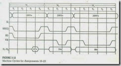
FIGURE 12
Machine Cycles for Assignments 19-23
17- Figure 12 shows the timings of three machine cycles. Identify the types of operations.
18- Do the three machine cycles in Figure 12 represent a complete instruction? Explain.
19- Examine the machine cycle M, in Figure 12 and specify the memory being accessed and its contents.
20- Does the byte on the data bus in the machine cycle Mil in Figure 12 represent an opcode?
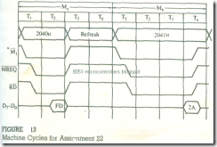
FIGURE 13
21- Explain what is being done in machine cycle Mc (Figure 12).
22- Identify the machine cycles Ma and Mb in Figure 13.
23- Identify the machine cycles in the following instructions:
SUB B : 1 By tell Machine Cycle/4 T-states
: Subtract the contents of register B from the accumulator
AND 47H : 2 B/2 MC/(4, 3) T-states
: Logically AND 47H with the contents of the accumulator
LD A, (2050H) : 3 B/4 MC/13 (4, 3, 3, 3) T-states
: copy the contents of the memory location 2050H into the accumulator
PUSH BC : 1 B/3 MC/10 (4, 3, 3) T-states
: copy the contents of BC register into two stack memory locations
Machine Cycles for Assignment 22


