SEMICONDUCTORS
Semiconductors, as the name implies, are materials that are neither good conductors nor good insula- tors. Semiconductors are made from materials that
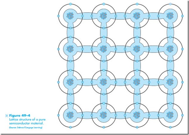
more often because of its ability to withstand heat. When semiconductor materials are refined into a pure form, the molecules arrange themselves into a crystal structure that has a definite pattern, Figure 49–4. A pattern such as this is known as a lattice structure.
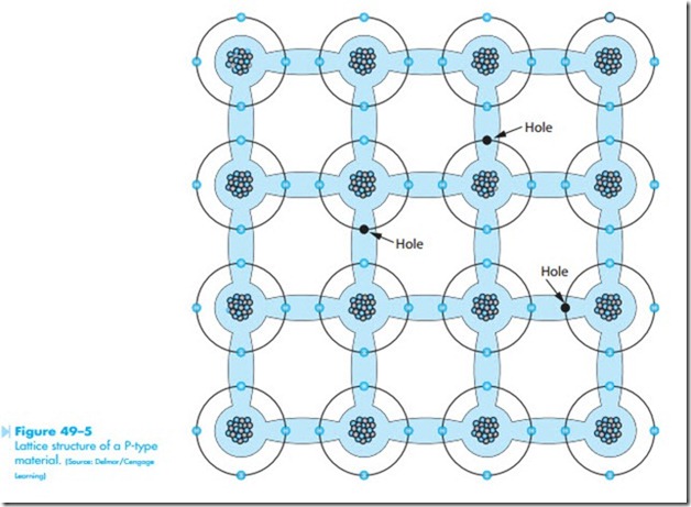
A pure semiconductor material such as silicon has no special properties and will do little more than make a poor conductive material. If a semiconductor material is to become useful for the production of solid-state components, it must be mixed with an impurity. When the semiconductor material is mixed with an impurity that has only 3 valence electrons, such as idium or gallium, the lattice structure also becomes different, Figure 49–5. When a material that has only 3 valence electrons is mixed with a pure semiconductor, a hole is left in the material when the lattice structure is formed. This hole is caused by the lack of an electron where one should be. Because the material now has a lack of electrons, it is no longer electrically neutral. Electrons are negative particles. Because a hole is in a place where an electron should be, the hole has a positive charge. This semiconductor material now has a net positive charge, and is therefore known as a P-type material.
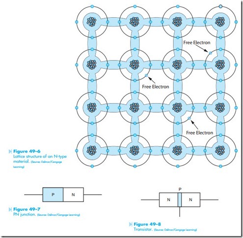
When a semiconductor material is mixed with an impurity that has 5 valence electrons, such as arsenic or antimony, the lattice structure will have an excess of electrons, Figure 49–6. Because electrons are negative particles, and there are more electrons in the material than there should be, the material has a net negative charge. This material is referred to as an N-type material because of its negative charge.
All solid-state devices are made from a combination of P- and N-type materials. The type of device formed is determined by how the P- and N-type materials are connected or joined together. The number of layers of material and the thickness of various layers play an important part in determining what type of device will be formed. For instance, the diode is often called a PN junction because it is made by joining together a piece of P-type and a piece of N-type material, Figure 49–7.
The transistor, on the other hand, is made by joining three layers of semiconductor material, Figure 49–8. Regardless of the type of solid-state device being used, it is made by the joining together of P- and N-type materials.


