Loss Model with Chip Number Information
In most of the cases, a series of IGBT modules at certain voltage rating is composed of different amounts of IGBT and diode dies/chips/cells, which are paralleled together in order to achieve various current ratings. The datasheets of the IGBT modules as well as the used chips are available on the website of semiconductor manufacturers [16], from which the 4.5 kV series IGBT modules which consist of different numbers of IGBT chips (4.5 kV/55 A) and freewheeling diode chips
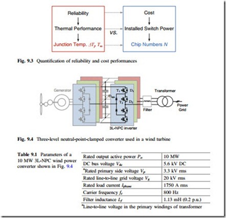
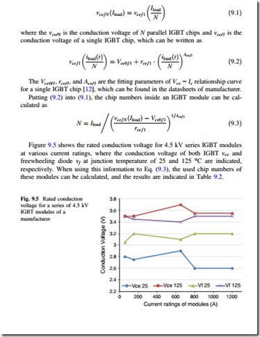
(4.5 kV/110A) are chosen as an example in this special topic [14]. The current ratings of these series IGBT modules range from 150 to 1200 A. A grid-side 10 MW three-level Neutral-Point-Clamped (3L-NPC) wind power converter is chosen and designed as a case study in this special topic, as shown in Fig. 9.4, and the detailed converter parameters are shown in Table 9.1 [1–3].
A. Chip Number Extraction from IGBT Modules
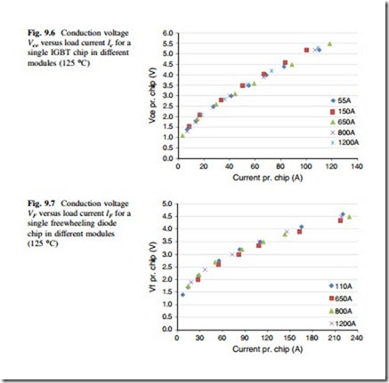
Unlike the switching behavior, the conduction voltage of both IGBT and diode is a relative “clean” characteristic which only depends on the junction temperature at the suggested gate drive voltage, while the switching characteristic depends not only on the junction temperature, but also on drive resistance, commutated voltage, di/dt, line inductance, etc. [11]. Normally, the used chip numbers of an IGBT module is not provided by the manufacturer in the datasheet; however, it is possible to calculate the chip numbers N according to the module’s conduction voltage at a certain load current Iload.
If the load current is equally distributed in each IGBT/diode chip, the total conduction voltage with N paralleled chips at the load current of Iload should be equal to the conduction voltage of a single IGBT/Diode chip at the load current of Iload/N, and this relationship can be written as
B. Conduction Loss Model with Chip Number Information
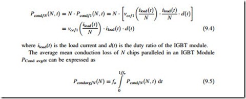
With the chip numbers in Table 9.1, it is possible to acquire the conduction voltage characteristic for a single chip inside the IGBT modules with different current ratings. Figures 9.6 and 9.7 show the conduction voltage–load current of a single IGBT and freewheeling diode chip in different rating modules listed in Table 9.1. It can be seen that the conduction voltage characteristic of a single IGBT or Diode chip inside different current rating modules are quite consistent with each other.
Therefore, the instantaneous conduction loss of N chips paralleled IGBT module Pcond/N can simply be expressed as the sum of conduction loss for each single chip Pcond/1:
Fig. 9.6 Conduction voltage Vce versus load current Ic for a single IGBT chip in different modules (125 °C
C. Switching Loss Model with Chip Number Information
As mentioned before, the switching loss characteristic of power devices depends on many factors, such as the drive resistance, di/dt, line inductance, etc. These factors are sensitive to the operating conditions and can be easily deviated when different numbers of chips are packaged. Therefore, it is inaccurate to calculate the switching loss of N chips paralleled IGBT module by simply summing up the switching loss of each single chip.
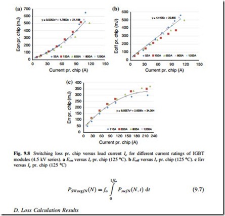
The solution is to investigate the switching loss characteristic pr. chip inside various current ratings of IGBT modules, and then an average Loss-Current curve is chosen to be summed up to get the total switching loss of N paralleled chips. With the information of chip numbers in Table 9.1, the switching loss characteristic pr. chip inside various current rating modules is plotted in Fig. 9.8. It can be seen that the switching loss characteristic pr. chip of different rating modules slightly deviates from each other. An average curve is chosen and fitted with two order functions as indicated in Fig. 9.8.
With the fitting function for the average switching loss characteristic pr. chip, the instantaneous switching loss of N chips paralleled IGBT module can be calculated as
The instantaneous loss of the most stressed switching devices for the 3L-NPC grid-side inverter under rated condition is shown in Fig. 9.9, where the chip number N is 22 and switching frequency is 800 Hz. The average losses of the most stressed switching devices with relation to the chip numbers are shown in Fig. 9.10.
